Tektronix 475 Technical Manual
Hide thumbs
Also See for 475:
- Instruction manual (251 pages) ,
- Instruction manual (72 pages) ,
- Instruction manual (55 pages)
Table of Contents
Advertisement
TM 11-6625-2735-14-1
TECHNICAL MANUAL
OPERATOR'S, ORGANIZATIONAL,
DIRECT SUPPORT AND GENERAL
SUPPORT MAINTENANCE MANUAL
FOR
OSCILLOSCOPE OS-261B(V)1/U
(NSN 6625-01-101-1318)
(TEKTRONIX MODEL 475 WITH OPTION 04)
This copy is a reprint which includes
current
pages from Change 1.
H E A D Q U A R T E R S, D E P A R T M E N T O F T H E A R M Y
JUNE 1982
Advertisement
Chapters
Table of Contents
Troubleshooting

Related Manuals for Tektronix 475


Summary of Contents for Tektronix 475
- Page 1 DIRECT SUPPORT AND GENERAL SUPPORT MAINTENANCE MANUAL OSCILLOSCOPE OS-261B(V)1/U (NSN 6625-01-101-1318) (TEKTRONIX MODEL 475 WITH OPTION 04) This copy is a reprint which includes current pages from Change 1. H E A D Q U A R T E R S, D E P A R T M E N T O F T H E A R M Y...
- Page 3 DEPARTMENT OF THE ARMY Washington, DC, 10 September 1984 No. 1 OPERATOR’S, ORGANIZATIONAL, DIRECT SUPPORT, AND GENERAL SUPPORT MAINTENANCE MANUAL OSCILLOSCOPE OS-261B(V)1/U (TEKTRONIX MODEL 475 WITH OPTION 04) (NSN 6625-01-101-1318) OSCILLOSCOPE OS-261C(V)1/U (TEKTRONIX MODEL 475 WITH OPTION 04 AND OPTION 07) (NSN 6625-01-119-7314) TM 11-6625-2735-14-1, 17 June 1982, is changed as follows: 1.
- Page 4 By Order of the Secretary of the Army: JOHN A. WICKHAM JR. General, United States Army Chief of Staff Official: ROBERT M. JOYCE Major General, United States Army The Adjutant General To be distributed in accordance with DA Form 12-36B requirements for 0S-261.
- Page 5 TM 11-6625-2735-14-1 SAFETY SUMMARY This manual contains safety information which the user must follow to ensure safe operation of this instrument. WARNING information is intended to protect the operator; CAUTION information is intended to protect the instrument. The following general safety precautions must be observed during all phases of operation, service, and repair of this instrument.
- Page 6 TM 11-6625-2735-14-1 SAFETY SUMMARY (CONT.) WARNING Adequate ventilation should be provided while using TRICHLOROTRIFLUOROETHANE. Prolonged breathing of vapor should be avoided. The solvent should not be used near heat or open flames; the products of decomposition are toxic and irritating. Since TRICHLOROTRIFLUOROETHANE dissolves natural oils, prolongted contact with skin should be avoided.
- Page 7 TM 11-6625-2735-14-1 SAFETY STEPS TO FOLLOW IF SOMEONE IS THE VICTIM OF ELECTRICAL SHOCK DO NOT TRY TO PULL OR GRAB THE INDIVIDUAL IF POSSIBLE, TURN OFF THE ELECTRICAL IF YOU CANNOT TURN OFF THE ELECTRICAL POWER, PULL, PUSH, OR LIFT THE PERSON TO SAFETY USING A WOODEN POLE OR A ROPE OR SOME OTHER INSULATING MATERIAL SEND FOR HELP AS SOON AS POSSIBLE AFTER THE INJURED PERSON IS FREE OF CONTACT WITH THE...
- Page 8 TM 11-6625-2735-14-1 WARNING HIGH VOLTAGE is used in the operation of this equipment DEATH ON CONTACT may result if personnel fail to observe safety precautions Never work on electronic equipment unless there is another person nearby who is familiar with the operation and hazards of the equipment and who is competent in administering first aid.
- Page 9 TM 11-6625-2735-14-1 SAFETY PRECAUTION A periodic review of safety precautions in TB 385-4, Safety Precautions for Maintenance of Electrical/Electronic Equipment, is recommended. When the equipment is operated with covers removed, DO NOT TOUCH exposed connections or components. MAKE CERTAIN you are not grounded when making connections or adjusting components inside the test instrument.
- Page 11 This manual contains copyright material reproduced by permission of Tektronix, Inc. TM 11-6625-2735-14-1 HEADQUARTERS ECHNICAL ANUAL DEPARTMENT OF THE ARMY No. 11-6625-2735-14-1 Washington, DC, 17 June 1982 OPERATOR’S, ORGANIZATIONAL, DIRECT SUPPORT, AND GENERAL SUPPORT MAINTENANCE MANUAL OSCILLOSCOPE OS-261B(V)1/U (TEKTRONIX MODEL 475 WITH OPTION 04)
-
Page 12: Table Of Contents
TM 11-6625-2735-14-1 TABLE OF CONTENTS Page MAINTENANCE (cont) Page INTRODUCTION SECTION 0 CABINET AND RACK ADAPTER REMOVAL Standard Cabinet Removal GENERAL INFORMATION AND SECTION 1 Standard Cabinet Installation INSTALLATION Rack Adapter Removal Introduction Rack Adapter Installation Characteristics PREVENTIVE MAINTENANCE 1-13 Installation Introduction Cleaning... - Page 13 MATERIALS LIST OF ILLUSTRATIONS Fig. Page Fig. Page Oscilloscope OS-261B(V)1/U and OS-261C(V)1/U Locations of circuit boards in the 475 Delay Time and Differential Time Measurement 4-23 Oscilloscope. Accuracy (Detailed) Locations of power transformer secondary Regulating Range Selector and Line Fuse.
- Page 14 TM 11-6625-2735-14-1 LIST OF ILLUSTRATIONS (CONT.) Fig. Page Page Fig. FO-10 Timing and Horizontal Display Switching Located FO-1 Block Diagram Located back of Schematic Diagram back of Manual FO-2 Channel 1 Vertical Preamplifier Schematic Manual FO-11 Horizontal Amplifier Schematic Diagram Diagram FO-12 Low Voltage Power Supply Schematic...
-
Page 16: Oscilloscope Os-261B(V)1/U And Os-261C(V)1/U
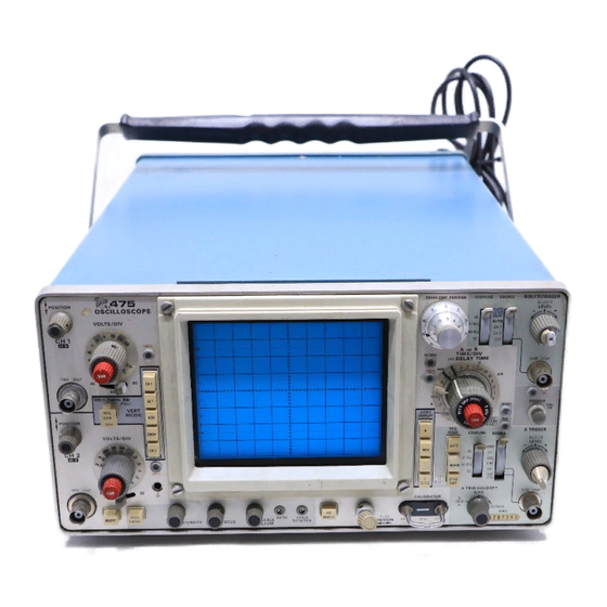
TM 11-6625-2735-14-1 Fig. 1-1. Oscilloscope OS-261B(V)1/U and OS-261C(V)1/U. Fig. 1-1.1. Oscilloscope, OS-261B and OS-261C(V)1/U, Power Supply -1106 Battery Pack. -
Page 17: Introduction
4610.33C/AFR 75-18/MCO tion and maintenance. Throughout this manual, the P4610.19D/DLAR 4500.15. OS-261B(V)1/U is referred to as Tektronix Model 475 with option 04, and the OS-261C(V)1/U is referred to as Tek- Reporting Equipment Improvement Recommendations tronix Model 475 with option 07. -
Page 19: General Information And Installation
Introduction complex digital words. The horizontal deflection system The 475 Oscilloscope is a 200 megahertz bandwidth has calibrated sweep rates from 0.5 second to 0.01 portable instrument designed to operate in a wide range of microsecond/division. - Page 20 TM 11-6625-2735-14-1 TABLE 1-1 ELECTRICAL Supplemental Information Performance Requirements Characteristics VERTICAL DEFLECTION SYSTEM (CH 1 and CH 2) 2 mV to 5 V/DIV in 11 steps; 1-2-5 Deflection Factor Calibrated sequence. Range CH 2 VERT SIGNAL OUT into CH 1 Deflection Factor to Approximately Cascaded Operation (CH 2 VERT input.
- Page 21 TM 11-6625-2735-14-1 TABLE 1-1 (cont) ELECTRICAL Performance Requirements Supplemental Information Characteristics VERTICAL DEFLECTION SYSTEM (cont) Step Response Positive-Going Step Aberrations (0°C to 40°C) +4%, –4%, 4% P-P At 5 mV/DIV Add 3% to positive-going step Negative-Going Step aberrations. Add 3% to positive-going step Added Mode aberrations.
- Page 22 TM 11-6625-2735-14-1 TABLE 1-1 (cont) ELECTRICAL Performance Requirements Supplemental Information Characteristics TRIGGER SYSTEM Sensitivity 0.3 div internal or 50 mV external DC Coupled from DC to 40 MHz, increasing to 1.5 div internal or 250 mV external at 200 MHz. 0.3 div internal or 50 mV external AC Coupled from 60 Hz to 40 MHz, increasing to...
- Page 23 TM 11-6625-2735-14-1 TABLE 1-1 (cont) ELECTRICAL Performance Requirements Supplemental Information Characteristics TRIGGER SYSTEM (cont) LEVEL Control Range At least + and –2 V, 4 V P-P. At least + and –20 V, 40 V P-P. Exclude LF REJ coupling mode. Trigger View ±20%.
- Page 24 TM 11-6625-2735-14-1 TABLE 1-1 (cont) ELECTRICAL Performance Requirements Supplemental Information Characteristics HORIZONTAL DEFLECTION SYSTEM (cont) MAGNIFIED Accuracy specification applies over the UNMAGNIFIED Calibrated Sweep Accuracy full 10 divisions of deflection unless otherwise specified. + 20°C to +30°C For all sweeps; exclude the first 25 ns when checking 0.01 and 0.02 div un- A or B DLY’D Sweep...
-
Page 25: Delay Time And Differential Time Measurement
11-6625-2735-14-1 TABLE 1-1 (cont) ELECTRICAL Supplemental Information Characteristics Performance Requirements HORIZONTAL DEFLECTION SYSTEM (cont) Within 0.5 division from graticule center Magnified Registration at 1 ms/DIV when switching X10 magnifier from on to off. POSITION Control Range Start of sweep must position to right of graticule center. - Page 26 TM 11-6625-2735-14-1 TABLE 1-1 (cont) ELECTRICAL Performance Requirements Supplemental Information Characteristics X-Y OPERATION Extreme counterclockwise position of Sensitivity Same as vertical deflection system. TIME/DIV switch. CH 2 OR X-Y button of VERT MODE switch must be pushed Deflection Accuracy Same as vertical deflection system. Variable Range Same as vertical deflection system.
- Page 27 TM 11-6625-2735-14-1 TABLE 1-1 (cont) ELECTRICAL Performance Requirements Supplemental Information Characteristics SIGNAL OUTPUTS CH 2 VERT SIGNAL OUT One division of deflection gives ap- proximately 20 mV into 1 M load. Output Voltage One division of deflection gives ap- proximately 10 mV into 50 load. Approximately 50 Output Resistance Bandwidth...
- Page 28 TM 11-6625-2735-14-1 TABLE 1-1 (cont) ELECTRICAL Supplemental Information Characteristics Performance Requirements CATHODE-RAY TUBE At least 15 Iines/division Horizontal Resolution At least 15 lines/division. Vertical Resolution 8 x 10 cm. Display Area 0.1 division or less of tilt or Geometry bowing. 0.1 division or less.
- Page 29 TM 11-6625-2735-14-1 TABLE 1-2 ENVIRONMENTAL Performance Requirements Supptemental Information Characteristics Temperature Operating (AC) –15°C to +55°C. Storage –55°C to +75°C. Altitude To 15,000 feet. Maximum operating Operating temperature decreased 1°C/1,000 feet above 5,000 feet. Storage To 50,000 feet. Humidity (Operating and Stor- 5 cycles (120 hours) referenced to MIL-E-16400F.
- Page 30 Export Shipping Weight Approximately 48.0 pounds (21.8 kg). Standard Accessories Standard accessories supplied with the 475 are listed in the Mechanical Parts List, in this Service manual. For optional accessories available for use with the 475, see the Tektronix, Inc., catalog. 1-12...
-
Page 31: Installation
TM 11-6625-2735-14-1 Installation The oscilloscope can be operated where the ambient air temperature is in the range of -28° C to +65° C, and can The following paragraphs include instructions for be stored where the temperature range is -62° C to +75° C. unpacking, inspecting, and installing the instrument, and After storage at temperatures outside of the operating the basic information required to operate the oscilloscope... -
Page 33: Operating Information
TM 11-6625-2735-14-1 Section 2—475 Service OPERATING INFORMATION PRELIMINARY INSTRUCTIONS Operating Power Sources This instrument can be operated from either a 115 volt or 230 volt nominal line voltage source, 48 to 440 Hertz. Introduction The Line Voltage Selector switch in the instrument... -
Page 34: Options
General The major controls and connectors for operation of the 475 are located on the front panel of the instrument. A few auxiliary functions are provided on the rear panel. Fig. 2-2 shows the front and rear panels of the 475. A brief description of each control and connector is given here. - Page 35 TM 11-6625-2735-14-1...
- Page 36 TM 11-6625-2735-14-1 100 (MHz): When TRIG VIEW Input connector for Channel 2 CH 2 OR Y button is pulled to the first de- deflection signals or Y-axis tent (100 indicated on yellow deflection in the X-Y mode of band of TRIG VIEW knob) the operation.
-
Page 37: A And B Triggering
TM 11-6625-2735-14-1 C H 2 O R X - Y : D i s p l a y s CH 2: Any signal that is dis- Channel 2 only. Must be pushed played in CH 2 of VERT MODE, when operating in X-Y mode. in full bandwidth position, is viewed with an increase in signal amplitude. - Page 38 TM 11-6625-2735-14-1 NORM: With the proper trigger 10 (A Trigger circuit control settings, A Sweep can only): External trigger signal be initiated by signals that are attenuated by a factor of 10. within the frequency range selected by the COUPLING switch.
-
Page 39: Calibrator And Power
TM 11-6625-2735-14-1 MIX: The first part of the A AND B TIME/DIV A TIME/DIV switch (clear AND DELAY TIME plastic outer flange) selects the horizontal sweep is displayed at a rate set by the A TIME/DIV basic delay time to be multiplied switch and the latter part of the by the DELAY TIME POSITION sweep at a rate set by the B... -
Page 40: Rear Panel
Regulating The following instructions will allow the operator who Range Selector assembly. is unfamiliar with the operation of the 475 to obtain the basic displays commonly used. Before proceeding with these instructions, preset the instrument controls as... -
Page 41: Magnified Sweep Display
TM 11-6625-2735-14-1 3. Advance the INTENSITY control until the display is 5. Set the HORIZ DISPLAY switch to B DLYD. The intensified zone on the display noted in step 3 is now being visible. If the display is not visible with the INTENSITY displayed in delay form. -
Page 43: Circuit Description
CHANNEL 2 PREAMP This section of the manual describes the circuitry used Page 3-6 General in the 475 Oscilloscope. The description begins with a First Cascode Amplifier Page 3-7 discussion of the instrument, using a basic block diagram. Next, each circuit is described in detail, using detailed... -
Page 44: Block Diagram
Delaying Sweep Generator before the individual circuits are discussed in detail. A Main Gate Amplifier Page 3-17 basic block diagram of the 475 Oscilloscope is shown in Page 3-17 Sweep Disconnect Amplifier Fig. 3-1. Only the basic interconnections between the... - Page 45 TM 11-6625-2735-14-1...
-
Page 46: Channel 1 Preamp
Horizontal Amplifier circuit through slope, coupling, and source controls. the Channel 1 Vertical Preamplifier circuit. There are three sweep generator circuits in the 475. For purposes of explanation, they are called Delaying, Slow Non-Delaying, and Fast Non-Delaying. The Delaying The Z Axis Amplifier circuit determines the CRT Sweep generates a range of sweep rates from 0.5 second... -
Page 47: Input Coupling
U120. U120 basically consists of an The effective overall deflection factor of each channel integrated emitter-coupled, push-pull, cascode amplifier of the 475 is determined by the appropriate VOLTS/DIV and two discrete field-effect transistors (FET) mounted on switch setting. The basic deflection factor of the Vertical a ceramic substrate with the thick-film resistors. -
Page 48: Channel 2 Preamp
TM 11-6625-2735-14-1 This input amplifier stage contains the CH 1 VAR The gain of U140 is determined by biasing the output VOLTS/DIV control. This control provides continuously transistors connected to pins 6 and 8 to conduct more or variable (uncalibrated) vertical deflection factors between less current. -
Page 49: Vertical Channel Switching
TM 11-6625-2735-14-1 VERTICAL CHANNEL SWITCHING First Cascode Amplifier Basically, the First Cascode Amplifier stage in Channel General 2 operates as described for the First Cascode Amplifier stage in Channel 1. However, the Channel 2 First Cascode The Vertical Channel Switching circuit determines Amplifier also contains the INVERT switching function. -
Page 50: Channel Switch Ic
TM 11-6625-2735-14-1 Channel Switch IC U370 also makes available samples of the Channel 1 signal at pins 8 and 9 and samples of the Channel 2 signal The Channel Switch IC U370 determines which of the at pins 4 and 5. The output signals at pins 4, 5, 8, and 9 are Preamp signals will be passed to the Vertical Output always present when signals are applied to the channel Amplifier. -
Page 51: Vertical Output Amplifier
TM 11-6625-2735-14-1 With a cable or an X1 probe connected to the CH 1 OR X Two Megahertz Clock input connector, the probe coding ring terminal on the U330C and U330D form an astable multivibrator having connector is not contacted, and therefore presents an a repetition rate of two megahertz. -
Page 52: A Trigger Generator
TM 11-6625-2735-14-1 A TRIGGER GENERATOR Second IC Amplifier The second amplifier stage in the Vertical Output General Amplifier is integrated circuit U470. U470 is a multi-stage cascode amplifier cell. The input signal is applied to pins 1 The A Trigger Generator circuit produces the trigger and 5 with the inverted output signal taken from pins 9 and pulse used to start the Sweep Generator circuit that 12. -
Page 53: Trigger Source
11-6625-2735-14-1 when the LEVEL control is centered. The LEVEL control Trigger Source varies the level at pin 14 of U520 to select the point on a Trigger SOURCE switch S505 selects the source of the trigger signal where triggering occurs. trigger signal. -
Page 54: B Trigger Generator
TM 11-6625-2735-14-1 The amplifier consists of two emitter-coupled push- Trigger Source pull amplifier stages. The emitter source voltage for Q662 The B Trigger Generator circuit has no LINE or EXT and Q672 is switched on and off by the TRIG VIEW 10 positions on its Trigger SOURCE switch. -
Page 55: Sweep Control Integrated Circuit
TM 11-6625-2735-14-1 Pin 4. This is the negative tunnel diode output terminal; Sweep Control Integrated Circuit connected to +5 volts in this application. U600 is the Sweep Control Integrated Circuit. Several functions are performed in this stage, depending on the Pin 5. -
Page 56: Main Gate Comparator
TM 11-6625-2735-14-1 Pin 9. Ground terminal. Delayed Gate Comparator Q802 and Q804 form the Delayed Gate Comparator and are connected as a voltage comparator where both Pin 10. This is the holdoff output; connected to ground transistors do not conduct at the same time. The input in this application, signal to the stage is the positive-going trigger signal from the B Firing Trigger TD in the B Trigger Generator circuit. -
Page 57: Delaying Sweep Latch Circuit
TM 11-6625-2735-14-1 Triggering SOURCE switch is in the STARTS AFTER MIX or A INTEN positions of the HORIZ DISPLAY switch, DELAY TIME position, the negative movement at the some additive unblinking is accomplished to slightly increase the intensity of the B portion of the display. In collector of Q792 reverse biases CR811, letting the –8volt supply pull down on the base of Q804 in the Delayed Gate these positions of the switch, –8 volts is connected to the... -
Page 58: Sweep Generators (And) Timing
TM 11-6625-2735-14-1 SWEEP GENERATORS The Sweep Generators produce the sawtooth voltages that are amplified by the Horizontal Amplifier to provide TIMING AND HORIZONTAL DISLAY horizontal deflection on the CRT. These sawtooth voltages are produced on command (trigger pulses) from SWITCHING the Trigger Generator circuits. -
Page 59: Delaying Sweep Generator
TM 11-6625-2735-14-1 Delaying Sweep Generator Sweep Disconnect Amplifier Basically the Delaying Sweep Generator is composed Q904 is the Sweep Disconnect Amplifier. The biasing of Q904, Q920, Q922, and Q914. This generator runs in the on the base of this stage determines whether the Delaying A INTEN, MIX, and B DLY’D positions of the HORIZ Sweep Generator will run. -
Page 60: Sawtooth Sweep Generator
TM 11-6625-2735-14-1 Delaying Sweep End Difference Amplifier Sawtooth Sweep Generator Q920 and Q922 forma Miller integrator circuit. When Q944 and Q946 are connected as a voltage comparator the current through the Sweep Disconnect Amplifier Q904 and generate the logic pulses that signal the end of sweep is interrupted, timing capacitance C, begins to discharge and blank the CRT display at the end of the sweep. -
Page 61: Non-Delaying Sweep Generators
TM 11-6625-2735-14-1 The sawtooth voltage waveform from the Delaying Non-Delaying Sweep Generator Differences Sweep Generator is connected to the gate of Q926B. The Basically the Non-Delaying Sweep Generators operate quiescent level of the delaying sawtooth biases Q926B on in the same manner as the Delaying Sweep Generator. and its drain is negative enough to bias Q938B on. -
Page 62: Horizontal Amplifier
TM 11-6625-2735-14-1 knob of TIME/DIV) is unlocked and set to a faster sweep In the A INTEN position of the HORIZ DISPLAY switch, rate, the Non-Delaying Sweep Generator is then being +5 volts is connected to the anode of CR1049. This used to display A Sweep. -
Page 63: Low-Voltage Power Supply
TM 11-6625-2735-14-1 Input Paraphase Amplifier Output Amplifier Q1124 and Q1134 form the Input Paraphase Amplifier. The push-pull signal from the Gain Setting Amplifier is This is an emitter-coupled amplifier stage that converts connected to the Output Amplifier. Each half of the Output the single-ended input signal to a push-pull output signal. - Page 64 TM 11-6625-2735-14-1 3-22...
-
Page 65: Power Input
12A or T1400 are intended for use with the optional pin 3. The difference in voltage levels is amplified and Inverter Circuit Board (Option 7) or for use with a 475 polarity is inverted by U1418. The result is that voltage Oscilloscope modification, a Power Supply Board (475 increases at pin 1 of U1418. -
Page 66: Crt Circuit
TM 11-6625-2735-14-1 +5-Volt Supply. Basic operation of all stages in the +5- +110-Volt Supply. CR1412 functions as a full-wave Volt Supply is the same as described in the +50-Volt center-tapped rectifier and provides an unregulated out- Supply and the +15-Volt Supply. The +5 volt reference for put voltage (approximately +136 volts) for the +110-Volt Power Supply. -
Page 67: High-Voltage Oscillator
TM 11-6625-2735-14-1 Hiigh-Voltage Regulator High Voltage Oscillator Feedback from the CRT cathode –2450 volt supply is Q1318 and associated circuitry compose the high- voltage oscillator that produces the drive for high-voltage applied to the base of Q1306 through R1303A. Any change transformer T1320. -
Page 68: High-Voltage Rectifiers And Output
TM 11-6625-2735-14-1 Q1312 and Q1310 compose an overvoltage protection increase in positive voltage. When the secondary-winding circuit. In the event the regulating action of the circuit output swings negative, CR1373 turns off, then CR1371 should cause the CRT cathode supply to approach turns on and clamps the less positive voltage swing at approximately –3000 volts, the voltage level at the emitter C1372 to the voltage level of the Z-Axis Amplifier. -
Page 69: Calibrator
A schematic of this circuit is shown on Diagram 13 at the rear of this manual. The fan motor used in the 475 is a brushless DC motor using Hall Effect devices. The fan motor control circuitry varies the rotational speed of the fan as the operating temperature changes. -
Page 71: Maintenance
, p r e v e n t i v e m a i n t e n a n c e , troubleshooting and corrective maintenance of the 475. Adjustment Locations Illustrations Page 4-6... -
Page 72: Cabinet And Rack Adapter Removal
Vertical Output Board Removal Page 4-26 Page 4-26 Fan Motor Board Removal Inverter Board Removal (Option 7 only) Page 4-27 Power Supply Board Removal (475 DM 43 Page 2-47 and DM 40 only) Page 4-28 Main Interface Board Removal Page 4-29... -
Page 73: Standard Cabinet Installation
Disconnect the instrument power cord from the power source and remove any interconnecting cables. 3. 475 DM-series only—lf the DM-series main circuit- board is not in place, install the board on the main chassis. NOTE It it is desired to tilt the Rack Adapter and Instrument, 4. -
Page 74: Rack Adapter Installation
2. If the Vertical Output circuit-board cover is not in breakdown and improves the reliability of this instrument. place, install the cover on the top of the 475 main chassis. The severity of the environment to which the 475 is Check all sections of the instrument where parts were subjected wiII determine the frequency of maintenance. -
Page 75: Switch Contacts
6. Coat the dry filter with an air-filter adhesive. Exterior. Loose dust accumulated on the outside of the 475 can be removed with a soft cloth or small paint brush. The paint brush is particularly useful for dislodging dirt on 7. -
Page 76: Visual Inspection
Each main circuit is assigned a series of component numbers. Table 4-1 lists the main circuits in the 475 and the series of component numbers assigned to Lubrication each. Important voltages and waveforms are also shown The fan motor and most of the potentiometers used in on the diagrams. -
Page 77: Troubleshooting Equipment
Tektronix Part Number using the resistor color-code system (e g , a diode color-coded pink — or — blue—, brown —gray—green indicates Tektronix Troubleshooting Equipment Part No 152-0185-00). -
Page 78: Color Codes For Resistors And Capacitors
11-6625-2735-14-1 RESISTORS CAPACITORS DIPPED , TANTALUM SIGNIFICANT COLOR VOLTAGE TOLERANCE FIGURES MULTIPLIER TOLERANCE MULTIPLIER RATING (pF) (OHMS) OVER 10pF UNDER 10pF — — – ±20% ±2pF 4VDC BLACK ±1% ±1% BROWN ±0.1pF 6VDC – — — ±2% ±2% or 100 10VDC or 100 ±3%... - Page 79 TM 11-6625-2735-14-1...
-
Page 80: Troubleshooting Techniques
If the trouble is not located by these checks, the Recommended type: Tektronix 576 Curve Tracer or remaining steps aid in locating the defective component. Tektronix 577 (D1 or D2) Curve Tracer with 177 Test When the defective component is located, it should be Fixture. -
Page 81: Check Circuit Board Interconnection
475 can be checked this way. A transistor can the page until a step is found which does not produce the be most effectively checked by substituting a new compo- indicated results. -
Page 84: Special Troubleshooting Information
ATTENUATORS. The thick film attenuators are best ing voltages and waveforms around the IC’s so that checked by substitution. If only one channel of the 475 is adjacent leads are not shorted together. A convenient not operating properly, and there is reason to believe an means of clipping a test probe to the 14- and 16-pin IC’s is... -
Page 85: Troubleshooting The L.v. Power Supplies
Connect the 475 to a variable autotransformer. Then, check each power supply for correct ripple with a test When repairing a power supply in the 475 the following oscilloscope, while varying the autotransformer Information may be helpful. The +50-volt supply is used as throughout the regulating range of this instrument (see an example to identify component functions. -
Page 86: Troubleshooting The High-Voltage Circuit
TM 11-6625-2735-14-1 2. Check that the current-limiting transistor is off Troubleshooting the Sweep Circuits. The sweep cir- cuits should be repaired in the following order: (Q1432 in the +50 volt supply) by measuring base-to- emitter voltage. If the supply is current limiting, remove A (Sweep) the power from circuit boards, individually, until the A INTEN (Intensified Sweep) - Page 87 TM 11-6625-2735-14-1 B DLY’D Sweep and Logic Now, pin 3 of U600 should have a low auto gate voltage. Check TP572 for approximately 0 volt. Check pin 16 of The A Sweep and A INTEN sweep should be working U600 for approximately 0 volt. Check pin 17 of U600 for properly before starting this procedure.
-
Page 88: Corrective Maintenance
TM 11-6625-2735-14-1 Troubleshooting the Horizontal Amplifier. T h e Vertical Channel Switch Troubleshooting Horizontal Amplifier contains push-pull circuitry that can The collector voltages of Q178 and Q188 must by be checked in the following manner: balanced as detailed in the preceding steps before starting Set TIME/DIV to 1 ms (lock knobs) and set TRIG MODE this procedure. -
Page 89: Obtaining Replacement Parts
475. If a higher wattage- each lead during machine insertion of the compo- rating soldering iron is used on the etched circuit boards, nent in the circuit-board manufacturing process. -
Page 90: Small Component Replacement
TM 11-6625-2735-14-1 3. Bend the leads of the new component to fit the holes If it becomes necessary to solder in the general area of in the board If the component is replaced while the board any of the high-frequency contacts in the instrument, is mounted in the instrument, cut the Ieads so they will just clean the contacts immediately upon completion of the protrude through the board. -
Page 91: Interconnecting Pin Replacement
TM 11-6625-2735-14-1 NOTE unsolder the pin (use a vacuum-type resoldering tool or a solder-removing wick to remove excess solder). Then After replacing a power transistor, check that the straighten the tabs on the socket and remove it from the collector is not shorted to ground before applying hole in the board. -
Page 92: Circuit Board Replacement
TM 11-6625-2735-14-1 If a cam switch must be removed from a circuit board 3. If the spacers come out with the strip, remove them the circuit board containing the cam switch must be from the stud pins for use on the new strip (spacers should removed from the instrument. - Page 93 TM 11-6625-2735-14-1 4-23...
-
Page 94: Vertical Preamp Board Removal
INVERT switch and J349) using a 15-Watt soldering iron. 1. 475 DM 43 and DM 40 only—Disconnect three ribbon-cables from the DM 43 or DM 40 Main circuit board. Remove the screws from the rear of the Main circuit board 8. -
Page 95: Trigger Generator And Z-Axis Logic Board Removal
Remove the board as follows: 1. 475 DM 43 and DM 40 only—Disconnect three ribbon-cables from the DM 43 or DM 40 Main circuit 3. Remove the VAR and VOLTS/DIV knobs. Set these board. -
Page 96: Timing Board Removal
TM 11-6625-2735-14-1 5. Remove the Timing circuit-board from the instru- Cable to J706 is white with a yellow stripe. ment. Use caution to prevent damage to the connecting pins on bottom of the board. Cable to J664 is white with black and brown stripes. To install the Timing circuit-board, reverse the removal procedure, Cable to J674 is white with black and red stripes. -
Page 97: Inverter Board Removal (Option 7 Only)
2. Disconnect one ribbon-cable from the rear of the 4. Remove two thread-forming screws nearest the Fan 475 DM 43 or DM 40 Main circuit-board and guide the plug Motor circuit-board, that hold the fan motor mount to the through a slotted opening in the main circuit-board main chassis. -
Page 98: Main Interface Board Removal
TM 11-6625-2735-14-1 f. Disconnect a four-wire cable at the rear of the A Main Interface Board Removal. If repair is necessary on the reverse side of the Main Interface circuit-board, it may TRIG HOLDOFF control (cable from the DELAY TIME be possible to gain access to that area by removal of one or POSITION control). -
Page 99: Power Transformer Removal
TM 11-6625-2735-14-1 f. Wire to the –2450 test point is solid red. Perform repairs on the reverse side of the Main Interface board, if repair is intended. To reinstall the board, reverse the removal procedure. If intentions are to replace the Main Interface circuit-board, continue with g. -
Page 100: Cathode-Ray Tube Removal
When storing a crt, place it in a protective 6. 475 DM 43 and DM 40 only—Unsolder five wires carton or set it face down on a smooth surface in a... -
Page 101: Cathode-Ray Tube Installation
6. Disconnect the four vertical deflection plate leads 8. 475 DM 43 and DM 40 only–install the DM 43 or DM from the Vertical Output board at the crt neck pins. -
Page 102: Delay Line Removal
TM 11-6625-2735-14-1 To install the Delay Line, reverse the removal 11. Hold the crt base socket away from the neck shield and slide the shield to the rear of the instrument about procedure. Use the Cathode-ray Tube Installation procedure for installing the crt. 2 inches. - Page 103 TM 11-6625-2735-14-1 TABLE 4-5 CALIBRATION INTERACTION AFTER REPAIR OR ADJUSTMENT 4-33/(4-34 blank)
-
Page 105: Performance Check Equipment Alternatives
475. Specifications given for the test equipment are suffice. Then check the Usage column to see what this item is used for. If used for a check or adjustment that is of the minimum necessary for accurate calibration. - Page 106 Description Specifications Usage Examples 1. Amplitude Calibrator Amplitude accuracy, within Vertical checks. Trigger view a. Tektronix PG 506 Cali- gain check; External Z-Axis 0.25%; signal amplitude, 2 bration Generator. millivolts to 20 volts; output check. signal, 1 kilohertz square b. Tektronix 067-0502-01 wave.
- Page 107 16. 10X Probe Scale factor check. Cali- Scale-factor switching; con- a. Tektronix P6075 Probe nector, ENC. brator check. (supplied with 475 oscil- loscope). b. Tektronix P6065 Probe. 17. 500 MHz Filter Impedance, 50 ohms; fre- Used for High-Speed Timing a Tektronix 500 MHz Filter quency, adjustable;...
-
Page 108: Operating Voltage
FOR PERFORMANCE CHECK Warm Up Operating Voltage Turn on the 475 and allow at least 20 minutes before Before applying power to the instrument, check that the starting the Performance Check procedure. line voltage selector and the regulating range selector are in the correct positions for the line voltage the instrument will be operated on. -
Page 109: Display And Vertical System Check
TM 11-6625-2735-14-1 DISPLAY AND VERTICAL SYSTEM CHECK 10X BNC Attenuator Equipment Required 1. Amplitude Calibrator 50-Ohm BNC Termination (2 required) 2. Sine-Wave Generator BNC Female-to-BNC Female Adapter 3. 42-inch 50-Ohm BNC Cable (2 required) BNC T-Connector 4. 18-inch 50-Ohm BNC Cable (2 required) 10. - Page 110 TM 11-6625-2735-14-1 i. CHECK—For no vertical deflection and that trace is k. CHECK—For control of graticule illumination from at center horizontal graticule line. minimum to maximum settings. j. Set CH 2 AC-GND-DC switch to AC. I. Set the amplitude calibrator for a 20 millivolt output and connect to CH 1 input through a 42-inch 50-ohm BNC cable.
- Page 111 TM 11-6625-2735-14-1 e. Return CH 2 VAR VOLTS/DIV to calibrated detent. d. ADJUST—CH 1 GAIN, 5 mV adjustment, through the upper 5 mV access hole at left side of cabinet for 4 divisions of amplitude. f. Set VERT MODE to CH 1 and move signal cable to CH 1 input.
- Page 112 TM 11-6625-2735-14-1 9. Check Bandwidth Limit Operation b. Position the 2 traces approximately 4 divisions apart. a. Set 100 OR 20 MHz BW control to 100. NOTE c. CHECK—That the traces alternate at all settings of If may be necessary to change sine-wave TIME/DIV except X-Y.
-
Page 113: Trigger System Check
TM 11-6625-2735-14-1 TRIGGER SYSTEM CHECK 8. GR-To-BNC Male Adapter Equipment Required Sine-Wave Generator 9. BNC Female-To-BNC Female Adapter Low-Frequency Generator 10. BNC Elbow Amplitude Calibrator 11. BNC T-Connector 50-Ohm Signal Pickoff 12. 10X BNC Attenuator 42-inch 50-Ohm BNC Cable 13. 5X BNC Attenuator 18-inch 50-Ohm BNC Cable (2 required) 14. - Page 114 TM 11-6625-2735-14-1 u. Set the low-frequency generator for a 3 division, f. CHECK—That a stable triggered display can be 60 Hertz display, then set CH 1 VOLTS/DIV to 50 mV. obtained in AC and DC positions of A TRIGGER COUPLING with adjustment of A TRIGGER LEVEL. v.
-
Page 115: 12. Check B Low-Frequency Triggering
TM 11-6625-2735-14-1 CHECK—Repeat part d of this step. ai. CHECK—That a stable triggered display cannot be obtained with adjustment of A TRIGGER LEVEL. Set CH 1 VOLTS/DIV to 10 mV. aj. Set CH 1 VOLTS/DIV to 5 mV, set TIME/DlV to 2 and set A TRIGGER SOURCE to NORM. -
Page 116: 13. Check B 40 Megahertz Triggering
TM 11-6625-2735-14-1 z. Set the low-frequency generator for a 1 division, b. Set the sine-wave generator for a 1 division, 60 Hertz display (50 millivolts at external input). (It may be 40 megahertz display, then set B TRIGGER SOURCE to necessary to maintain triggering as amplitude is reduced.) EXT (50 millivolts at external input). -
Page 117: Check A 200 Megahertz Triggering
TM 11-6625-2735-14-1 f. Set TIME/DIV to 0.1 ms and set A TRIGGER d. CHECK—That a stable triggered display can be SOURCE to EXT. obtained in CH 1 and CH 2 positions of A TRIGGER SOURCE with adjustment of A TRIGGER LEVEL. g. -
Page 118: 17. Check Trig Mode Norm Operation
TM 11-6625-2735-14-1 f. Set B TRIGGER SOURCE to STARTS AFTER 18. Check TRIG MODE SINGL SWP Operation DELAY and set TIME/DIV to 1 Return the test signal cable to CH 1 input. Press and release SINGL SWP pushbutton. g. Set the sine-wave generator for a 1.5 division, 200 megahertz display. -
Page 119: Horizontal System Check
TM 11-6625-2735-14-1 HORIZONTAL SYSTEM CHECK 4. 500 MHz Filter Equipment Required 1. Time-Mark Generator 5. 42-inch 50-Ohm BNC Cable (2 required) 6. 50-Ohm BNC Termination (2 required) 2. Sine-Wave Generator 3. Amplitude Calibrator 7. 10X Probe (see Table 5-1, 10X Probe examples) Sweep Control Settings POWER... -
Page 120: Check Sweep Length And Horizontal Position Range
TM 11-6625-2735-14-1 c. CHECK—TIME/DIV settings from 10 ms to 21. Check Sweep Length and Horizontal 0.5 s/division for accuracy, at first and 11th graticule lines, POSITION Range within 2%, from +20°C to +30°C; within 3%, from –15°C a. Set time-mark generator for 1 millisecond time to +55°C. -
Page 121: 26. Check Differential Delay Time Accuracy
TM 11-6625-2735-14-1 c. Set CH 1 VOLTS/DIV to maintain a convenient c. Turn DELAY TIME POSITION to 1.000. Adjust horiz- display amplitude and set A TRIGGER LEVEL for a stable ontal POSITION to set time mark at center graticule line. display. -
Page 122: 27. Check Delay Time Jitter
TM 11-6825-2735-14-1 TABLE 5-4 Delay Time Settings DELAY TIME A TIME/DIV B TIME/DIV Time-Mark Switch Generator POSITION Switch Setting Setting Setting Exclusions 0.01 Exclude dial 0.05 50 nanosecond 0.01 0.1 microsecond settings of 0.02 0.2 microsecond 0.000 through 1.000 0.05 0.5 microsecond 1 microsecond 2 microsecond... -
Page 123: Gate Outputs, External Z-Axis And Calibrator Checks
TM 11-6625-2735-14-1 30. Check X Bandwidth 29. Check X Gain a. Set TRIG MODE to AUTO, set DLY’D SWP to lock NOTE knobs, set TIME/DIV to X-Y, set VERT MODE to CH 2 and set X (CH 1) VOLTS/DIV to 5 mV. See test equipment required, Table 5-1, for selection sine-wave generator... -
Page 124: 31. Check A And B +Gate Outputs
TM 11-6S25-2735-14-1 g. Set CH 1 VOLTS/DIV to 50 mV and insert a 50-ohm 31. Check A and B +GATE Outputs termination between CH 1 input and the connected BNC a. Connect A +GATE (output connector on rear panel) cable. to CH 1 input through a 42-inch 50-ohm BNC cable. -
Page 125: Schematic Diagrams & Options 04 And
TM 11-6625-2735-14-1 Section 6—475 Service SCHEMATIC DIAGRAMS AND OPTIONS 04 AND 07 Symbols and Reference Designators Electrical components shown on the diagrams are in the following units unless noted otherwise: Values one or greater are in picofarads (pF). Capacitors = Values less than one are in microfarads ( F). - Page 126 Cathode ray tube mesh filter installed to minimize crt This section describes the features of Option 04 as it faceplate radiation. pertains to the 475 Oacilloscope. This circuitry modifies the instrument to meet conducted and radiated in- terference requirements over the frequency range of 150 kHz to 25 MHz (conducted) and 150 kHz to 1 GHz (radiated).
- Page 127 OPTION 7 Permits 12 V operation of the instrument from DC 12 Option 7 is a dc to ac inverter that permits Tektronix an external 12 V source. Oscilloscopes to operate on 12 or 24V dc with no performance deterioration. Circuitry is provided to protect...
- Page 128 11-6325-2735-14-1 Source voltages higher than 22 V dc cause increased Simplified Block Diagram current through R1607, Q1606 and R1609. Q1608 is kept See Figure 6-2. The dc source is applied to the turn-off cut off by the increased voltage across R1609 and the level circuit, the start circuit and the primary of T1400.
- Page 129 TM 11-6625-2735-14-1 Start circuit Turn-Off Circuit When S1601 is closed, the external dc source is applied Q1622 is off under normal operating conditions until to C1614, VR1641, and R1645. The initial surge is coupled the dc source drops below 22 V and causes Q1622 to to Q1642 through C1614, VR1639, and R1641.
- Page 130 TM 11-6625-2735-14-1 Start-Stop Switch R1664, distribute the drive evenly between the four transistors, C1652, C1662, C1654 and C1664 degenerate S1601, Section A in the off (stop) position discharges the high frequency response and reduce transients. the capacitors in the turn-off and start circuits. This ensures the correct time constants when S1601 is chang- Feedback to maintain inverter operation is provided ed to the on (start) position.
- Page 131 TM 11-6625-2735-14-1 Circuit Board Chassis Removal 3. 1106 Power Supply battery pack. The circuit board is mounted on a small chassis located between the power transformer and the crt shield. To remove the chassis, remove three screws. Two thread- 4. Two 12-volt wet-cell storage batteries, in series, forming screws are located at the top of the chassis.
- Page 132 TM 11-6625-2735-14-1 6-2.6 Change 1...
- Page 133 TM 11-6625-2735-14-1 Operate the oscilloscope in the 24 V mode. Set the dc b. Change the dc source to 12 V. Operate the os- source to 24 V. Connect the test oscilloscope between cilloscope in the 12 V mode. Vary the dc source from 14 V C1801 (C) and the common negative return (A).
- Page 134 TM 11-6625-2735-14-1 6-28 Change 1...
-
Page 135: Replaceable Mechanical Parts
TM 11-6625-2735-14-1 Section 7—475 Service REPLACEABLE MECHANICAL PARTS PARTS ORDERING INFORMATION Detail Part of Assembly and/or Component Attaching parts for Detail Part For complete part information refer to TM 11-6625-2735-24P-1. - - - * - - - Parts of Detail Part... - Page 136 TM 11-6625-2735-14-1...
- Page 137 TM 11-6625-2735-14-1 Change 1 7-3...
- Page 138 TM 11-6625-2735-14-1...
- Page 139 TM 11-6625-2735-14-1...
- Page 140 TM 11-6625-2735-14-1 7 - 6...
- Page 141 TM 11-6625-2735-14-1...
- Page 142 TM 11-6625-2735-14-1...
- Page 143 TM 11-6625-2735-14-1...
- Page 144 TM 11-6625-2735-14-1 7-10...
- Page 145 TM 11-6625-2735-14-1 7-11...
- Page 146 TM 11-6625-2735-14-1 7-12...
- Page 147 TM 11-6625-2735-14-1 7-13...
- Page 148 TM 11-6625-2735-14-1 7-14...
- Page 149 TM 11-6625-2735-14-1 Change 1 7-15...
- Page 150 TM 11-6625-2735-14-1 7-16...
- Page 151 TM 11-6625-2735-14-1 Change 1 7-17/(7-18 blank)
- Page 153 TM 11-6625-2735-14-1 7-19...
- Page 154 TM 11-6625-2735-14-1 7-20...
- Page 155 TM 11-6625-2735-14-1 7-21...
- Page 156 TM 11-6625-2735-14-1 7-22...
- Page 157 TM 11-6625-2735-14-1 7-23/(7-24 b l a n k )
- Page 159 TM 11-6625-2735-14-1 7-25...
- Page 160 TM 11-6625-2735-14-1 7-26...
- Page 161 TM 11-6625-2735-14-1 7-27/(7-28 blank)
- Page 163 TM 11-6625-2735-14-1 7-29...
- Page 164 TM 11-6625-2735-14-1 7 - 3 0...
- Page 165 TM 11-6625-2735-14-1 7-31...
- Page 166 TM 11-6625-2735-14-1 7-32...
- Page 167 TM 11-6625-2735-14-1 7-33...
- Page 168 TM 11-6625-2735-14-1 7-34...
-
Page 169: Appendix A References
TM 11-6625-2735-14-1 APPENDIX A REFERENCES The following is a list of applicable references that are available to the operator and maintenance personnel. DA Pam 310-1 Consolidated Index of Army Publications and Blank Forms. DA Pam 738-750 The Army Maintenance Management System (TAMMS). SB 38-100 Preservation, Packaging, Packing and Marking Materials, Supplies, and Equipment Used by the Army. -
Page 171: Introduction
TM 11-6625-2735-14-1 APPENDIX B COMPONENTS OF END ITEM LIST AND BASIC ISSUE ITEMS LISTS Section I. INTRODUCTION B-1. SCOPE (2) Item Number. The number used to identify item called out in the illustration. This appendix lists integral components of and basic issue items for Oscilloscope 0S-261B(V)1/U and 03-261C(V)1/U to help you inventory items required for safe and efficient b. - Page 172 TM 11-6625-2735-14-1 B-2 Change 1...
- Page 173 TM 11-6625-2735-14-1 SECTION Il. INTEGRAL COMPONENTS OF END ITEM Change 1 B-3...
-
Page 174: Integral Components Of End Item
TM 11-6625-2735-14-1 SECTION Il. INTEGRAL COMPONENTS OF END ITEM B-4 Change 1... - Page 175 TM 11-6625-2735-14-1 SECTION Il. INTEGRAL COMPONENTS OF END ITEM ILLUSTRATION ( 7 ) QUANTITY NATIONAL DESCRIPTION STOCK USED LOCATION NUMBER REQD RCVD DATE CODE PART NUMBER (FSCM) 6625-00-127-0079 OSCILLOSCOPE OS-261B(V)1/U and 0S-261C(V)1/U (80008) Consisting of: POUCH Top of 016-0535-02 (80009) oscilloscope ACCESSORY PACKAGE In pouch...
- Page 176 TM 11-6625-2735-14-1 SECTION Il. INTEGRAL COMPONENTS OF END ITEM QUANTITY ILLUSTRATlON NATIONAL DESCRIPTION LOCATION S T O C K REQD DATE RCVD N U M B E R FIG. ITEN (FSCM) PART NUMBER PROBE WITH ACCESSORIES In pouch 010-61-1-01 (80009) Consisting of: In pouch PROBE 010-6101-00 (80009) Consisting of:...
- Page 177 TM 11-6625-2735-14-1 SECTION Il. INTEGRAL COMPONENTS OF END ITEM ILLUSTRATION QUANTITY NATIONAL DESCRIPTION USED STOCK LOCATION ITEM NUMBER REQD RCVD DATE CODE PART NUMBER (FSCM) PROBE WITH ACCESSORIES In pouch 010-6106-01 (80009) Consisting of: PROBE In pouch 010-6106-00 (80009) Consisting of: PROBE HEAD On probe 206-0216-00 (80009) Consisting of:...
- Page 178 TM 11-6625-2735-14-1 SECTION III. BASIC ISSUE ITEMS Usable Description National Stock Illus On Code FSCM and Part number number number TECHNICAL MANUAL: TM 11-6025-2735-14-1...
-
Page 179: Maintenance Allocation
TM 11-6625-2735-14-1 APPENDIX D MAINTENANCE ALLOCATION Section I. lNTRODUCTION D-1. General Consists of comparisons of two instruments, one of which is a certified standard of known accuracy, to detect and adjust any discrepancy in the accuracy of the instrument This appendix provides a summary of the maintenance being compared. -
Page 180: Column Entries
TM 11-6625-2735-14-1 D-3. Column Entries e. Column 5, Tools and Equipment. Column 5 specifies by code, those common tool sets (not individual tools) and special tools, test, and support equipment required to a. Column 1, Group Number. Column 1 lists group perform the designated function. -
Page 181: Circuit
TM 11-6625-2735-14-1 SECTION Il. MAINTENANCE ALLOCATION CHART OSCILLOSCOPE 0S-261B(V)1/U AND OS-261C(V)1/U MAINTENANE CATEGORY TOOLS GROUP MAINTENANCE COMPONENT/ASSEMBLY NUMBER REMARKS FUNCTION EQPT. Impact OSCILLOSCOPE OS-261B(V)1/U Visual External AND 0S-261C(V)1/U Test Simple Opera- tional Calibrate 1 thru 29 Repair 1 thru 29 Repair 1 thru 29 Overhaul... - Page 182 TM 11-6625-2735-14-1 SECTION Il. MAINTENANCE ALLOCATION CHART OSCILLSCOPE OS-201B(V)1/U AND OS-201C(V)1/U MAINTENANCE CATEORY Inspect CIRCUIT CARD ASSY (A9) Test Replace Repair Inspect CIRCUIT CARD ASSY (A10) Test Replace Repair Inspect DC TO AC INVERTER (OPTION 07) Test Replace Repair D-4 Change 1...
-
Page 183: Oscilloscope
SIMPSON 269 OSCILLOSCOPE, TEST, OS-261B(V)1/U, EQUIVALENT TO 6625-00-127-0079 TEKTRONIX TYPE 475 AMPLITUDE CALIBRATOR, AN/USM-360, STANDARD, 6625-00-192-0866 EQUIVALENT TO TEKTRONIX 06741502-01 CAL. GEN. POWER SUPPLY, PP 7208/U, EQUIVALENT TO 6130-00-175-0832 LAMBDA LPD-422A-FM GENERATOR, MEDIUM-FREQUENCY CONSTANT- 6625-00-520-5143 AMPLITUDE SIGNAL, EQUIVALENT TO TEKTRONIX... -
Page 184: Oscilloscope Os-261B(V)1/U And
TEKTRONIX PART No. 011-0069-02 TERMINATION (50 OHM FEED THRU), 2 EA, 5985-00-087-4954 EQUIVALENT TO TEKTRONIX PART No. 011-0049-01 FILTER, 500 MHz, EQUIVALENT TO TEKTRONIX PART No. 067-0684-00 5935-00-482-1776 ADAPTER, CONNECTOR, BNC MALE TO MINIATURE PROBE TIP, EQUIVALENT TO TEKTRONIX PART No. -
Page 185: Remarks
TM 11-0625-2735-14-1 SECTION IV. REMARKS REFERENCE REMARKS CODE Replace lamps and knobs. D-7/(D-8 blank) -
Page 187: Appendix Eexpendable Supplies And Materials List Introduction
TM 11-6625-2735-14-1 APPENDIX E EXPENDABLE SUPPLIES AND MATERIALS LIST Section I. INTRODUCTION E-1 . SCOPE This appendix lists expendable supplies and materials you will need to operate and maintain the oscilloscope. These items are authorized to you by CTA 50-970, Expendable Items (Except Medical, Class V, Repair Parts, and Heraldic Items). E-2. -
Page 188: Expendable Supplies And Materials
TM 11-6625-2735-14-1 SECTION Il. EXPENDABLE SUPPLIES AND MATERIALS NATIONAL STOCK ITEM DESCRIPTION LEVEL NUMBER NUMBER Brush, paint 8 0 2 0 - 0 0 - 7 2 1 - 9 6 5 7 7 9 2 0 - 0 0 - 8 6 2 - 6 7 1 0 Cloth, lint-free P a i n t S a n d p a p e r... - Page 214 By Order of the Secretary of the Army E. C. MEYER General, United States Army Official: Chief of Staff ROBERT M. JOYCE Brigadier General, United States Army The Adjutant General DISTRIBUTION: To be distributed in accordance with Special List. GOVERNMENT PRINTING OFFICE : 1989 0 - 242-451 (1654)
- Page 217 PIN : 051123-000...
Need help?
Do you have a question about the 475 and is the answer not in the manual?
Questions and answers