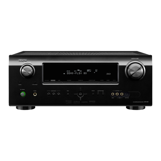
Denon AVR-591 Service Manual
Hide thumbs
Also See for AVR-591:
- Owner's manual (224 pages) ,
- Manual del usuario (76 pages) ,
- Specifications (2 pages)
Table of Contents
Advertisement
Quick Links
e
AVR-591
• For purposes of improvement, specifications and design are subject to change without notice.
• Please use this service manual with referring to the operating instructions without fail.
• Some illustrations using in this service manual are slightly different from the actual set.
S0035-1V01DM/DG1003
SERVICE MANUAL
MODEL
AV SURROUND RECEIVER
Copyright 2010 D&M Holdings Inc. All rights reserved.
WARNING: Violators will be prosecuted to the maximum extent possible.
JP
E3
E2
P
e
D&M Holdings Inc.
Ver. 1
EK
EA
E1
E1K E1C
Advertisement
Table of Contents

Related Manuals for Denon AVR-591


Summary of Contents for Denon AVR-591
- Page 1 Ver. 1 SERVICE MANUAL MODEL E1K E1C AVR-591 AV SURROUND RECEIVER • For purposes of improvement, specifications and design are subject to change without notice. • Please use this service manual with referring to the operating instructions without fail. • Some illustrations using in this service manual are slightly different from the actual set.
-
Page 2: Safety Precautions
SAFETY PRECAUTIONS The following check should be performed for the continued protection of the customer and service technician. LEAKAGE CURRENT CHECK Before returning the unit to the customer, make sure you make either (1) a leakage current check or (2) a line to chassis resistance check. - Page 3 NOTE FOR SCHEMATIC DIAGRAM WARNING: Parts marked with this symbol z have critical characteristics. Use ONLY replacement parts recommended by the manufacture CAUTION: Before returning the unit to the customer, make sure you make either (1) a leakage current check or (2) a line to chassis resistance check. If the leakage current exceeds 0.5 milliamps, or if the resistance from chassis to either side of the power cord is less than 460 kohms, the unit is defective.
-
Page 4: Technical Specifications
TECHNICAL SPECIFICATIONS n Audio Section Usable Sensitivity : • Power amplifier [FM]1.2 μV (12.8 dBf) [AM]18 μV Rated output : 50 dB Quieting Sensitivity : Front : 75 W + 75 W (8 Ω, 20 Hz – 20 kHz with 0.08 % T.H.D.) [FM]MONO 2.8 μV (20.2 dBf) 120 W + 120 W (6 Ω, 1 kHz with 0.7 % T.H.D.) S/N (IHF-A) : Center : 75 W (8 Ω, 20 Hz – 20 kHz with 0.08 % T.H.D.) [FM]MONO 70 dB 120 W (6 Ω, 1 kHz with 0.7 % T.H.D.) STEREO 67 dB Surround : 75 W + 75 W (8 Ω, 20 Hz – 20 kHz with 0.08 % T.H.D.) Total harmonic Distortion (at 1 kHz) : 120 W + 120 W (6 Ω, 1 kHz with 0.7 % T.H.D.) [FM]MONO 0.7 % Output connectors : 6 – 16 Ω... -
Page 5: Surround Mode
SURROUND MODE 0 Service Jigs When you repair the printing board, you can use the following JIG (Extension cable kit). Please order to Denon Official Service Distributor in your region if necessary. 8U-110084S : EXTENSION UNIT KIT : 2 Set... - Page 6 DISASSEMBLY • Disassemble in order of the arrow of the figure of following flow. • In the case of the re-assembling, assemble it in order of the reverse of the following flow. • In the case of the re-assembling, observe "attention of assembling" it. • I f wire bundles are untied or moved to perform adjustment or parts replacement etc., be sure to rearrange them neatly as they were originally bundled or placed afterward. Otherwise, incorrect arrangement can be a cause of noise generation. CABINET TOP FRONT PANEL ASSY RADIATOR ASSY HDMI UNIT ASSY Refer to "DISASSEMBLY Refer to "DISASSEMBLY Refer to "DISASSEMBLY 1. FRONT PANEL ASSY" 2. RADIATOR ASSY" 4. HDMI UNIT ASSY" and "EXPLODED VIEW"...
-
Page 7: Front Panel Assy
1. FRONT PANEL ASSY Proceeding : CABINET TOP FRONT PANEL ASSY → (1) Remove the screws. View from bottom (2) Disconnect the connector wires and FFC cable, then remove the screws. STYLE PIN : Loose CP100 STYLE PIN : Loose FFC cable Please refer to "EXPLODED VIEW" for the disassembly method of each PCB included in FRONT PANEL ASSY. - Page 8 2. RADIATOR ASSY Proceeding : CABINET TOP RADIATOR ASSY → (1) Remove the screws. View from bottom (2) Remove the screws. Direction of Direction of photograph: C photograph: D STYLE PIN : Loose...
- Page 9 (3) Cut the wire clamp bands, then disconnect the connector wires and FFC cable. RADIATOR ASSY CP100 STYLE PIN : Loose N2706 FFC cable (4) Disconnect the connector wires. CP401 CP402 PCB 5CH AMP Please refer to "EXPLODED VIEW" for the disassembly method of each P.W.B included in RADIATOR ASSY.
- Page 10 3. PCB REG CNT/PCB REG Proceeding : CABINET TOP RADIATOR ASSY PCB REG CNT/PCB REG → → (1) Remove the screws. PCB REG (2) Disconnect the connector wires and connector board. CP102 CP104 PCB REG CNT CP13B Direction of photograph: C PCB REG Board to board CP13A...
- Page 11 4. HDMI UNIT ASSY Proceeding : CABINET TOP HDMI UNIT ASSY → (1) Disconnect the connector wire and FFC cable. FFC cable HDMI UNIT ASSY CX100 BACK PANEL (2) Remove the screws, then remove the BACK PANEL. Direction of photograph: A (3) Cut the wire clamp band, then disconnect the and connector wires. Remove the screw. CP401 N2501 N2706 CP13B CP13A HDMI UNIT ASSY...
- Page 12 (4) Remove the connector, then remove the HDMI UNIT ASSY from the main unit. CP12 Direction of photograph: D (5) Disconnect the connector board. Board to board Board to board PCB HDMI Board to board (6) Disconnect the connector board. PCB SIDE CNT Board to board PCB FRONT CNT Board to board PCB AUDIO VIDEO...
- Page 13 5. PCB SPK/PCB SMPS Proceeding : CABINET TOP HDMI UNIT ASSY PCB SPK/PCB SMPS → → (1) Remove the Sheet, then remove the screws and SUPPORTER P.C. SUPPORTER P.C. Sheet View from bottom (2) Disconnect the connector wire, then remove the screws. PCB SPK/PCB SMPS CX102...
- Page 14 (3) Disconnect the connector wire, then remove the screws. Remove the PCB SPK/PCB SMPS from the main unit. (4) Disconnect the connector board. PCB SPK PCB SMPS Board to board...
- Page 15 6. TRANS MAIN Proceeding : CABINET TOP TRANS MAIN → (1) Disconnect the connector wires, then remove the screws. CP100 STYLE PIN : Loose CX102 (2) Disconnect the connector wires. CP102, CP104...
- Page 16 SPECIAL MODE Special mode setting button b Press the ON/STANDBY button to turn on while pressing both buttons A and B at the same time. Mode Button A Button B Contents Firmware versions such as Main, Sub, DSP are displayed in µcom/DSP Version display mode STATUS DIMMER...
- Page 17 1. µcom/DSP Version display mode 1.1. Operation specifications µcom/DSP version display mode: When started up, the version information is displayed. Starting up: With the "DIMMER" and "STATUS" buttons pressed, press the "ON/STANDBY" button to turn the power on. Now, press the "STATUS" button to the display the 2nd item information on the FL Display. 1.2.
- Page 18 2. Errors checking mode (Displaying the protection history) 2.1. Operation specifications Error mode (Displaying the protection history): When started up, the error information is displayed. Starting up: ●All model commonness With the "STATUS" and "MULT EQ" buttons pressed, press the "ON/STANDBY" button to turn the power on. The error (protection history display) mode is set.
- Page 19 2.3. Clearing the protection history There are two ways to clear the protection history, as described below. (1) Start up the error (protection display) mode, display the error, then press and hold in the "ENTER" button for 3 seconds. : T H E R M A L T H E Press and hold in the "ENTER"...
- Page 20 When you repair the printing board, you can use the following JIG (Extension cable kit). Please order to DENON Official Service. Distributor in your region if necessary. Note: When the connection which is wrong in the JIG (EXTENSION UNIT KIT) is done it becomes cause of damage.
- Page 21 (4) Connect the four extension jig cables. PCB HDMI Insulation sheet PCB FRONT CNT PCB SIDE CNT Connection table of Board to Board Ref. No. Ref. No. 11 pin SIDE CNT N2709 HDMI 25 pin SIDE CNT N2708 HDMI 19 pin CP105 FRONT CNT N2701...
- Page 22 ABOUT REPLACE THE MICROPROCESSOR WITH A NEW ONE When replaced of the U-PRO (Microprocessor) or the Flash ROM, confirm contents of the following. After PWB Name Ref. No. Description Remark replaced DIGITAL U3102 R5F64169DFD SOFTWARE: Main DIGITAL U3301 R5F3650KNFB SOFTWARE: Sub DIGITAL U1903 EN29LV160BB-70TIP SOFTWARE: DSP ROM...
- Page 23 4. Run the DENON Flash ROM Writer Run the “FlashWriter7_001_forAVR1611_1911_2311.exe” on desktop of PC. 5. Communication check (1) Click the “Check communication” button. (2) When connection is good, then you can see the “Communication check OK.” message. (3) If connection is not good, then you can see the “Communication error!” message.
- Page 24 6. Download the firmware (1) Click the "Select" button. (2) Download the firmware from the specified download source to PC.
- Page 25 7. Complete the firmware updating (1) Click the “Update” button. (2) When writing of the firmware is completed, the power of this unit turns on automatically and you can see the “Update completed” message. (3) If you can’t complete the firmware update, please retry the firmware update from “3. Turn on the AV receiver/ amplifier”.
- Page 26 8. Notice: Please keep the following notice for firmware update. (a) Keep the PC environment (b) Avoid the communication cable from the electrical noise source. (e.g. telephone cable, AC line, a fluorescent light) (c) Don’t remove cable during update. (d) Don’t turn off the power during update. (e) Don’t run other PC application during update.
-
Page 27: Surround Modes And Parameters
SURROUND MODES AND PARAMETERS b ( v page zz ) Refer to the instruction manual. - Page 28 Simple version Basic version Advanced version Information...
- Page 30 Simple version Basic version Advanced version Information...
-
Page 31: Audio Section
ADJUSTMENT Audio Section Idling Current Required measurement equipment: DC Voltmeter 1. Preparation (1) Avoid direct blow from an air conditioner or an electric fan, and adjust the unit at normal room temperature 15 °C ~ 30 °C (59 °F ~ 86 °F). (2) Presetting • POWER (Power source switch) STANDBY... -
Page 32: Trouble Shooting
TROUBLE SHOOTING 1. POWER 1.1. Power not turn on Power not turn on. When the power turned on, does the ON/STANDBY Is the fuse blown? Refer to 1.2.Fuse is blown. indicator on the front panel flashing green? Is a DC 5V voltage output Check for damage in the SMPS B'D Is a DC 5V voltage being... -
Page 33: Analog Video
2. Analog video MONITOR OUT (CVBS) output NG Input CVBS Input S Input Function : SAT Function : DOCK COMPONENT To A To B Not output HDMI OUT outpu NG Input CVBS Input S Input COMPONENT Input Function : SAT Function : DOCK Function : SAT HDMI... - Page 34 Input CVBS Check power supply voltage. FRONT CONNECTOR B'D REGULATOR B'D flaw. V+5V : CP13B-4pin V-5V : CP13B-1pin Check on set value of each IC. HDMI B'D L2706 : H(5V) L2707 : L(0V) HDMI B'D flaw. L2708 : L(0V) L2709 : H(5V) L2710 : H(5V) L2711 : H(5V) Extend HDMI B'D using a jig.
- Page 35 Input Check power supply voltage. FRONT CONNECTOR B'D REGULATOR B'D flaw. V+5V : CP13B-4pin V-5V : CP13B-1pin Check on set value of each IC. HDMI B'D L2706 : L(0V) L2707 : L(0V) HDMI B'D flaw. L2708 : L(0V) L2709 : L(0V) L2710 : L(0V) L2711 : L(0V) Extend HDMI B'D using a jig.
- Page 36 Input CVBS/S/COMPONENT Check input signal of VIDEO DECODER HDMI B'D V : L2718 Check signal DET Input CVBS : to A S-Y : L2718 V/S_L2704 : H(+3.3V) Input S : to B S-C : L2719 COMPONENT_L2703 : H(+3.3V) Input COPONENT : to D COMPONENT-Y : L2717 COMPONENT-Cb : L2716 COMPONENT-Cr : L2715...
- Page 37 Check HDMI output setting, referring to the (5) Is the BD/DVD player's HDMI output setting correct? BD/DVD player's operating instructions. (6) When using a DENON BD/DVD player's, is the fluorescent display tube's "HDMI" indicator lit? If using a non-DENON BD/ DVD player's, proceed to "YES".
- Page 38 BD/DVD player, is the FL HDMI connector (K1001/K1002/K1003/ from the HDMI connector display's "HDMI" indicator lit? K1004)15pin(DDC_CLK)/16pin(DDC_DATA)? (K1001/K1002/K1003/ If using a non-DENON BD/ Is 1pin/3pin/4pin/6pin/7pin/9pin/10pin/12pin of K1004) to the U1001 is DVD player, proceed to HDMI connector (K1501) terminated by 3.3V and defective.
- Page 39 Check operation of each device. (AMP source : BD / Video input of player : 480P / Connect the TV.) Check operation of U1001. (18) Check power supply. Is 1.8V supplied to C1019/C1053/C1037/L1003? The power supply circuitry is defective. Is 3.3V supplied to C1112/C9032/C1124/C1122? (19) Check xtal oscillator.
- Page 40 2.2. HDMI test point and waveforms C9000 C9005 C9010 C9015 L2516 C9020 C2568 C2702 C2560 L2736 N2703 L2734 C2502 L2735 R2512 R2517 R2502 L2731 C9073 C9083 C2529 R2513 C2520 C2130 R2332 C2547 Q2517 Q2528 C2904 R2515 C2503 R2514 R2503 C2530 R2518 U2305 C9098...
- Page 41 DDC_CLK/DDC_DATA/TMDS(1,3,4,6,7,9,10,12pin) : Check item (15),(17) 0.9V DDC_CLK 2.48V DDC_DATA IPINDE/IPINVSYNC/IPINHSYNC/IPINPCK : Check item (21) 31.76us IPINDE IPINDE 31.84us IPINHSYNC IPINHSYNC 16.68ms IPINVSYNC IPINVSYNC IPINPCK 37.0ns...
- Page 42 1TXDE/1TXVSYNC/1TXHSYNC/1TXPCK : Check item (25) 31.76us 1TXDE 1TXDE 31.84us 1TXHSYNC 1TXHSYNC 16.68ms 1TXVSYNC 1TXVSYNC 1TXPCK 37.0ns...
- Page 43 4. AUDIO 4.1. AUDIO CHECK AUDIO OUTPUT : NG INPUT SURROND MODE SOURCE CHECK1 Check ANALOG AUDIO BLOCK. ANALOG 2CH DIRECT ANALOG INPUT SURROND MODE SOURCE CHECK2 Check Digital AUDIO BLOCK. COAX or OPT Legacy(PCM or DolbyDigital or dts…) INPUT SURROND MODE SOURCE CHECK3 Check via AD.
- Page 44 4.2. Power AMP (7CH AMP B'D) No sound is output. The protector operates. Is the power transistor open or short circuit? Replace the power transistor. 2SB1560/2SD2390 Is the emitter resistance of the power transistor open? Replace the emitter resistance. 0.47Ω Is the base resistance of the power transistor open? Replace the base resistance.
-
Page 45: Analog Audio
4.3. Analog audio No sound is output Is the voltage of ±8V supplied to The power supply of ±8V is repaired. AV B'D CP8? Is the audio signal transmitted to The power amplifier is repaired. AV B'D CN401? Connect the connectors properly. Is the serial data for electronic volume Is the connector correctly connected transmitted to AV B'D CP11? - Page 46 Personal notes:...
- Page 47 CLOCK FLOW & WAVE FORM IN DIGITAL BLOCK Wave form U1001 HDMI Rx ADV7840 CH1: D-DATA U1707 AUDIO PLD EPM3032ATC DIR/DIT U1706 LC89058W-E INPUT CH1: DATA COAXIAL-1 (2)RX0 SDIN(24) SLRCK(23) (42)SLRCK OPTICAL-1 (4)RX2 (37)256fsDIR RMCK(16) RBCK(17) (3)64fsDIR (9)RX5 RLRCK(20) (2)fsDIR CH2: fs RDATA(21) (44)DATADIR1...
- Page 48 BLOCK DIAGRAM AUDIO BLOCK DIAGRAM SPDIF 1TXSPDIF HDMI IN1 U1001(8U-310052) LRCK 1TXFS U1903(8U-310052) U1902(8U-310052) 1TX64FS INPUT SWITCHER MCLK 1TXMCLK RECEIVER EPROM I2S3 HDMI IN2 ADV7840 I2S2 16MBIT 64MBIT I2S1 I2S0 KEY_MATRIX RESONATOR RESONATOR HDMI IN3 FCX-03(16MHz) 1TXI2S0 ZTT16MHz 1TXI2S0 1TXI2S1 1TXI2S1 DIN_FLFR 1TXI2S2...
- Page 49 VIDEO BLOCK DIAGRAM HDMI 1.4VER REPEATER BLOCK HDMI-1 HDMI-2 U1501(8U-310052) AVR1611 ONLY ADV7511 HDMI HDMI IN MONITOR OUT HDMI Tx HDMI-3 U1001(8U-310052) ADV7840 HDMI Rx HDMI-4 DECODER IC811(AV B'D) SIGNAL DET. DOUBLER NJM2586M -6dB -6dB 75§Ù -6dB COMPONENT 75§Ù LOAD -6dB 75§Ù...
- Page 50 VCC BLOCK DIAGRAM MAIN +B S1(AMP +B) MAIN -B 7808 A+8.0V (Pre) DA+5.0V 7805 S2(+8V,-8V) A-8.0V (Pre) 7908 2388F09 A.TUNER+9.0V(E2/E1C/J) MAIN TRANS A.TUNER+5.0V(E3) 2388F05 7805 A.V+5.0V S4(VIDEO) A.V-5.0V 7905 -VKK S5(-VKK) FL AC (F1) AC CORD S6(FILAMENT) FL AC (F2) HD Radio+3.3V PQ033 CPUPOWER...
- Page 51 LAEVEL DIAGRAM LEVEL DIAGRAM FRONT ch R2A15220FP ANALOG H/POUT SPEAKER + LINE IN GAIN ADJ. + AK4358VQ + (NR1601,AVR3311 ONLY) AK5358B + - - MUTE PRE OUT ZONE2 (AVR2311/3311 ONLY) ZONE3 (AVR3311 ONLY) (AVR3311ONLY) RECOUT1 RECOUT2 EXT IN +30dB 4.34Vrms/8Ω SPK OUT FULL SCALE LEVEL=3Vrms AK4358VQ...
- Page 52 LEVEL DIAGRAM CENTER ch R2A15220FP SPEAKER + GAIN ADJ. AK4358VQ + + (AVR3311 ONLY) - - MUTE PRE OUT EXT IN +30dB 4.2Vrms/8Ω SP OUT MAX SIGNAL LEVEL +20dB +20dB 0dBFS=1.77Vrms +29dB +10dB +10dB -10dBFS L.P.F GAIN=+1.6dB 213mVrms EXT IN -3dB 200mV 0dB...
- Page 53 LEVEL DIAGRAM SUBWOOFER ch R2A15220FP SPEAKER + GAIN ADJ. AK4358VQ + + (AVR3311,SR5005/605/7005 ONLY) - - MUTE PRE OUT EXT IN +30dB 4.74Vrms SW ch DAC MAX SIGNAL LEVEL PRE OUT Config1(S/S/S/Y)DOLBY LIMIT LEVEL=2.5Vrms (5.1ch-3dBFS at 30Hz) +11dB AK4358VQ +20dB +20dB 0dBFS=1.77Vrms 1.37mVrms...
- Page 54 LEVEL DIAGRAM SURROUND ch R2A15220FP SPEAKER + GAIN ADJ. AK4358VQ + + (AVR3311,SR5005/6005/7005 ONLY) - - MUTE PRE OUT EXT IN +30dB 4.2Vrms/8Ω SP OUT MAX SIGNAL LEVE AK4358VQ +5dB +20dB +20dB 0dBFS=1.77Vrms +29dB +10dB +10dB -10dBFS L.P.F GAIN=+5dB 218mV -3dB 200mV 0dB...
- Page 55 LEVEL DIAGRAM SURR.BACK ch R2A15220FP SPEAKER + GAIN ADJ. AK4358VQ + + (AVR3311 ONLY) - - MUTE PRE OUT (AVR2311/3311 ONLY) from from ZONE2 ZONE2 from ZONE3 (AVR3311 ONLY) EXT IN (SR5005/6005/7005 ONLY) +30dB 4.2Vrms/8Ω SP OUT AK4358VQ MAX SIGNAL LEVE +20dB +20dB 0dBFS=1.77Vrms...
- Page 56 R2A15220FP LEVEL DIAGRAM SB-ch FRONT/ZONE ASIGN 0dB ZONE2/3 from F-ch from SPEAKER DA SB-ch + LINE IN + MAIN from EXT.IN SB-ch AVR2311/3311, ZONE2 NJW1194 ONLY TONE MONO MUTE PREOUT MONO AVR3311 ONLY ZONE3 NJW1194 TONE MONO MUTE PREOUT MONO +30dB SP OUT 4.48Vrms/8Ω...
- Page 57 PRINTED WIRING BOARDS 5CH-AMP (COMPONENT SIDE) 7CH AMP B'D G401 631010096006S WIRE 7020-06941-000-0S BONDING CLAMP 400 G400 G401 BKT400 CP401 WIRE WIRE J590 WIRE BONDING BONDING BONDING C408 R428 WIRE C456 C424 R687 G402 R601 BONDING R440 R558 C440 R472 C504 R471 R644...
- Page 58 SMPS (COMPONENT SIDE) D103 D25SC6M SMPS (FOIL SIDE) 鉛フリー半田 半田付けには、鉛フリー半田 (Sn-Ag-Cu) を使用してください。 Lead-free Solder When soldering, use the Lead-free Solder (Sn-Ag-Cu).
- Page 59 SPK (COMPONENT SIDE) JACK3 WIRE4 WIRE4 JACK1 WIRE5 WIRE5 RLY3 RLY5 RLY2 RLY6 RLY7 CP22 WIRE3 RLY4 7020-06942-201-0S SPK B'D CN13 BKT1 BAR CODE BKT3 WIRE1 WIRE2 WHITE(R) BLACK(L) WIRE3 RLY1 WIRE1 WIRE2 WHITE(R) BLACK(L) LIMIT- LIMIT- LIMIT+ LIMIT+ MUTE+7V RLGND RL+B RELAY_WIDE...
- Page 60 SPK (COMPONENT SIDE) 鉛フリー半田 半田付けには、鉛フリー半田 (Sn-Ag-Cu) を使用してください。 Lead-free Solder When soldering, use the Lead-free Solder (Sn-Ag-Cu).
- Page 61 REG (COMPONENT SIDE) FRONT_CNT (COMPONENT SIDE) CLAMP100 CLAMP101 CP105 C137 IC108 J118 R144 J116 C136 R129 7028-06943-301-0 D123 CP117 R126 FRONT CNT_B'D NJM2388F CP14 J104 V-5V CN15 BAR CODE J105 V_GND CN13 V_GND J106 V+5V -->CN104 CP116 C127 D115 R146 R145 J107 C126...
- Page 62 REG (FOIL SIDE) FRONT_CNT (FOIL SIDE) TRG_VGND TRG_15V TRG_15V +5V_IN +5V_IN VGND VGND -5V_IN -5V_IN TU_GND TU_GND TU_VOL_IN TU_VOL_IN REG_CNT (FOIL SIDE) Q100 Q101 鉛フリー半田 半田付けには、鉛フリー半田 (Sn-Ag-Cu) を使用してください。 Lead-free Solder When soldering, use the Lead-free Solder (Sn-Ag-Cu).
- Page 63 SIDE_CNT (COMPONENT SIDE) SIDE_CNT (FOIL SIDE) IC109 PQ033DNA1ZPH J101 CP802 M3.3V 232IMO 232OMI M/DGND BKT101 AZ4580 7028-06943-401-0 CP13A SIDE CNT_B'D AC MUTE DET AC MUTE DET X2 VOLT DET X2 VOLT DET DA+5V DA+5V TRG+15V TRG+15V TRG_GND TRG_GND A+8V A+8V A-8V A-8V AGND...
- Page 64 FRONT (COMPONENT SIDE) FRONT B'D 7028-06944-101-0 CP100_1 CP102 U101 JP93 C143 C142 U100 RMC100 C144 JP86 JP131 R108 LED101 JP72 C147 JP85 JP27 JP80 JP105 JP71 LED102 LED104 JP104 ZD101 DSXLED MTZ6.8B R192 JP103 C101 JP32 JP41 JP102 C102 C151 JP125 JP33 JP94...
- Page 65 FRONT (FOIL SIDE) C500 C501 R150 R149 C140 C503 C502 Q100 R110 R163 D107 C124 C125 C126 C139 C165 R172 C146 R159 R156 R154 R158 R157 D105 R111 R161 D109 C137 R160 R155 R153 R145 Q105 C111 R114 R173 R109 Q104 Q103 Q106...
- Page 66 AUDIO_VIDEO (COMPONENT SIDE) AUDIO_VIDEO (FOIL SIDE) R1068 IC812 C970 TC4053BFT R1051 C972 C969 C948 R1060 R1066 R1035 R1053 C971 R1052 R1054 CP1003 C968 IC811 NJM2586M C974 R1041 VGND Q831 C911 R1031 VDI_CR C952 R1032 VGND R1067 VDI_CB C961 VGND VGND VDI_CR VDI_PY VGND...
- Page 67 HDMI (COMPONENT SIDE) C9000 C9005 C9010 C9015 L2516 C9020 C2568 C2702 C2560 L2736 N2703 L2734 C2502 L2735 R2512 R2517 R2502 L2731 C9073 C9083 C2529 R2513 C2520 C2130 R2332 C2547 Q2517 Q2528 C2904 R2515 C2503 R2514 R2503 C2530 R2518 U2305 C9098 C9102 L2510 L2507...
- Page 68 HDMI (FOIL SIDE) R2126 R2160 C2144 R2159 C9078 C9068 C9058 C2511 C2512 C2510 Q2509 R2122 R2156 C2539 L2515 R2507 R2508 C2142 R2155 R2509 C2358 C2357 C2508 C2507 C2509 L2513 R2521 R2936 R2153 R2119 R2505 R2550 C2113 R2154 C2141 R2506 L2514 R2504 R2934 R2935...
- Page 69 PAGE 1 AMP B'D 1/2 R703:2.7K R703 R401 1.2K 1611/1911 ZD401 R402 R403 1.2K R404 R406 MTZJ5.1A 100K 270(1) R405 OPEN PRF18BC471QB5RB C401 270(1) OPTION_A 100N-K C402 Q401 D401 OPEN TP401 OPTION_D KTA1024Y C403 R407 1SS133T OPEN 10N-K C404 OPEN R412:47K 2311/3311 Q403...
- Page 70 PAGE 2 PAGE 2 AMP B'D 1/2_A10 PAGE 2 AMP B'D 1/2_M10 R706:2.7K R706 R531 ZD410 R532 1.2K 1611/1911 R533 1.2K R534 MTZJ5.1A 100K 270(1) R535 R537 270(1) 5.6K(1) PRF18BC471QB5RB C449 OPTION_A C450 Q437 OPTION_D D419 OPEN TP404 100N-K KTA1024Y 1SS133T OPEN C452 47/50...
- Page 71 PAGE 3 SPEAKER B'D JACK1 470(2) H/PR FR_GND SPK_SMPS 1/2 2200P 0.047 RLY1 FR_A BC3-12 FL_GND 2200P 0.047 H/PL 470(2) FL_A 0.5uH 0.047 C_GND 10(NB) 2200P 0.047 10(2) 0.5uH 0.047 10(NB) RLY2 G5PA-28-MC 12V JACK2 10(2) SR_GND 2200P 0.047 0.5uH SL_GND 0.047 2200P...
- Page 72 PAGE 4 SPK_SMPS 2/2 CX103 SMPS B'D OPEN POWER S/W OPTION J180 L100 L101 BKT102 JUMPER LF4ZBE273H OPEN F100 TH100 J100 JUMPER D100 1N4007 JK100 live J150 AC INLET OPEN ZD100 JUMPER D101 1N4007 ZD101 Neutral MTZJ22B (E3) ¡Ü ¡Ü MTZJ39B D103 D25SC6M...
- Page 73 PAGE 5 REGULATOR B'D REG_SIRIUS_COMMON CNT 1/4 D114 SCHOTTKY IC103 NJM7805FA VIDEO_+5V VIDEO_-5V CN14 IC104 NJM7905FA VIDEO-5V VIDEO_GND SCHOTTKY VIDEO_GND D117 VIDEO+5V D118 SCHOTTKY OPTION_C IC106 IC105 CP117 NJM7805FA NJM7808FA A+8V CN13 FUSE F104,F105,F106,F107,F108 RL GND AGND AVR1611/1911 RL +B TU_RTGND T1.6AL/250V NR1602...
- Page 74 PAGE 6 REG_SIRIUS_COMMON CNT 2/4 SIDE CONNECTOR TO RC-5 TO RC-5 PAGE 8(1B) PAGE 8(1A) OPTION A OPTION B MODEL MODEL AVR1611 AVR1611 AVR1911 AVR1911 OPTION_B AVR2311 AVR2311 AVR3311 AVR3311 SR5005 SR5005 OPTION_A SR7005 SR7005 IC109 C125Z2-15P C125Z2-19P PQ033DNA1ZPH AVR1911 E3 ONLY CP802 10/50 IC1A:A...
- Page 75 PAGE 7 REG_SIRIUS_COMMON CNT 3/4 FRONT CONNECTOR HDMI HDMI HDMI HDMI HDMI PAGE 20(2B) PAGE 20(2C) PAGE 20(4D) PAGE 20(4D) PAGE 20(4B) AVR16/1911 _ N.C CP110 CP107 CP108 CP106 TO HDMI CP105 CP109 AVR2311/3311, SR5005/7005 TO A_VIDEO CP113 CP112 CP111 AVR2311/3311, SR5005/7005 CP114...
- Page 76 PAGE 8 R418 D5V(MX) Q406 REG_SIRIUS_COMMON CNT 4/4 SWM5V(MX) KRA102S SWM3.3V R419 Q401 R401 OPEN(2W) Q404 M3.3V KRA102S KRC102S C419 C470 R402 OPEN(2W) D/MGND OPEN 4700N-K R403 OPEN(2W) SIRIUSMO R404 OPEN(2W) SIRIUSMI SIRIUSRST D401 A+8V KDS160 A+8V A-8V Q402 A-8V KRA102S R405 OPEN...
- Page 77 TO CONNECT SIDE TO CONNECT FRONT AV B'D(1/3) TO CONNECT FRONT PAGE 7(4E) PAGE 6(8E) PAGE 6(5E) TO CNT1 PAGE 7(6E) PAGE 3(1E) OPEN PAGE 9 CP10 CP11 CN402 11 10 6 5 4 3 2 H/P_L TO TUNER H/P_GND H/P_R RLY_F RLY_C...
- Page 78 PAGE 10 AV B'D(2/3) OPTION_D L1001 R1204 75J-207CX C872 R933 10/50 OPTION_A C1112 8.2N(R) R1200 R1063 C1111 Q824 4.7N(R) R934 R935 KRC231S 100K CP800 OPTION_B TUNERL TUNERL TUNERR TUNERR TO ANALOG TUNER BD801 BEAD TU_5V TU_3.3V/5V/9V R949 Q825 R936 R937 SCLK TU_TXMI/SCL L1000...
- Page 79 AV B'D(3/3) PAGE 11 CVBS OUTPUT SW (TC4052BF) C903 C904 INPUT 47/16 47/16 OUT PUT FUCTION C905 C906 X0 Y0 10N-K 10N-K X1 Y1 X2 Y2 X3 Y3 NONE NONE R951 V+5V Y/C_MIX MONI_SEL_A IC807:A D839 BD7628 MONI_SEL_B KDS4148U R958 75-D MONITOR R959...
- Page 80 PAGE 12 R1023 CEC_RX CEC_COM K1001 L1003 OPEN RXA_5V HDMI-CONNECTOR CEC1.8V AVDD1.8 D1045 OPEN A RXA_5V SHELL2 R1010 U1002 R1011 R1012 R1024 R1025 L1002 OPEN PQ018ENA1ZPH HPD/HEAC- BLM21PG221 IN 1 LRCLK RXD_2- RXD_1- RXD_0- RXD_C- CEC3.3V RXC_2- RXC_1- RXC_0- RXC_C- RXB_2+ RXB_1+ RXB_0+...
- Page 81 DV5V DV3.3V DV1.8V DGND IPINB0 IPINB0 IPINB1 IPINB1 IPINB2 IPINB2 IPINB3 PAGE 13 IPINB3 IPINB4 IPINB4 IPINB5 IPINB5 IPINB6 IPINB6 DV5V IPINB7 IPINB7 DV3.3V IPINB8 IPINB8 DV1.8V IPINB9 IPINB9 DGND IPINB10 IPINB10 IPINB11 IPINB11 IPSCL IPING0 IPING0 IPSDA IPING1 IPING1 IPING2 1TXVSYNC IPING2...
- Page 82 PAGE 14 1TXINT 1TXINT 1TXRST R1525 OPEN 1TXRST R1526 OPEN C1516 4.7/6.3 C1517 OPEN C1518 OPEN IPSCL IPSCL IPSDA IPSDA R1502 TX_VSYNC R1521 OPEN 1TXVSYNC CEC_CLK AVR1911/791 TX_HSYNC R1502 SR5005 ONLY 1TXHSYNC DVDD R1502 TX_DE C1501 0.1/10 C1519 0.1/10 DVDD 1TXDE DVDD R1504...
- Page 83 TO HDMI TX PAGE 15 TO SUB CPU TDIA ↓ AUDIOPLD X1701 FCX04(24.576MHZ) C1714 C1715 N1701 OPEN AUDIO1 R1743 DIR1PERR R1746 MCLK1 R1730 33x4 R1740 3.3K R1730 33x4 DIRDOUT R1739 DATAAD. DIRDIN R1730 33x4 SLRCK1 SLRCK DIRCE SBCK1 R1730 33x4 SBCK DIRCLK R1731...
- Page 84 TO DIR/PLD TO SUBCPU PAGE 16 R1945 CLKO. R1946 33x4 33x4 R1946 33x4 SDA10. R1946 C1969 R1946 33x4 0.1/10 1 VCC 33x4 R1947 SDWE. ED0. 2 DQ0 DQ15 ED15. R1974 68x4 R1970 68x4 33x4 ..CKE C1970 R1947 0.1/10 3 VCC 33x4 RAS.
- Page 85 TO DIR/PLD TO SUB CPU PAGE 17 C9151 1000P C9152 1000P C9153 DA+5V DA+7V DA-7V 1000P C9154 1000P R2135 R2136 C9155 C9059 C9074 C9068 C9088 1000P OPEN OPEN OPEN OPEN C9073 C9093 DA+5V OPEN OPEN DGND DAGND A+7V C9078 C9098 DA+7V C2107 0.1/10...
- Page 86 TO MAIN CPU PAGE 18 USB TCC8600 AVR1911/791/NR1601/SR5005 ONLY NET3.3V DIGITAL NET1.8V SUPPLY DGND R2311 4.7K R2348 R2312 4.7K U2305 C2356 C2359 AK4424ET 1/10 C2360 1/10 JTAG 4.7/6.3 N2301 L2303 OPEN VSS2 BLM21PG221 R2332 TCKUSB CVDD MCLKUSB GND_D1 MCLK TDOUSB BCKoUSB BICK VSS1...
- Page 87 PAGE 19 L2513 BLM21PG221 L2514 BLM21PG221 L2515 BLM21PG221 N2501 5P-BASE(SMW250) D5.2V D3.3V D5.2V DGND DGND AVR1911/791/NR1601/SR5005 ONLY L2516 11A121 MAINPOWER D3.3V L2501 L2507 500mA 20 PVIN BLM21PG221 VOUT OPEN 430mA D3.3V 430mA 21 PVIN NET3.3V VOUT Q2507 500mA TCC8600 U2504 22 NC U2501 NET1.8V...
- Page 88 TO DIGITAL SUPPLY PAGE 20 EMI FILTER MP=PATARN SHORT L2813 OPEN L2814 SWM5V OPEN L2815 OPEN REMOTE3.3V SWM3.3V L2816 OPEN L2817 M3.3V OPEN L2818 OPEN L2819 OPEN L2820 N2708 OPEN 25P-SOCKET(C125Z2) (C125Z2) L2721 OPEN D5V(MX) SWM5V(MX) SWM3.3V M3.3V DA+5V D/MGND DA+7V SIR_MO5/RDSDA L2790...
- Page 89 TO DIGITAL CONNECT PAGE 21 R2925 R2926 OPEN R2927 OPEN R2928 OPEN DIGITAL SUPPLY SWM3.3V REMOTE3.3V N2901 SWM5V 4P-FFCs R2937 4.7K M3.3V DGND 232MO 232I_MO COMP.SDET 232MI 232O_MI Z1VSIG.DET Z1SSIG.DET R2902 CEC_POWER R2903 SR5005 OPEN DV_POWER2 DA_POWER DV_POWER1 232IMO3 DV_POWER1 DA_POWER 232OMI3 DV_POWER2...
- Page 90 TO_LEVEL_CHG PAGE 22 SWM3.3V R3151 4.7K M3.3V R3152 4.7K DGND MAINPOWER MAINPOWER M_RESET M_RESET BDOWN BDOWN U3103 MICDET R1EX24256ASAS0A Q3101 P11/D9 P43/A19 RELAY_H/P KRC102S R3138 4.7Kx4 CLKSIMO P10/D8 P44/A20 CLKSIMO RELAY_H SIMO P07/D7 P45/A21 SIMO MUTE_Z2 ACKSIMO P06/D6 P46/A22 ACKSIMO MUTE_SB RSTSUB P05/D5...
- Page 91 TO HDMI RX PAGE 23 TO I/P TO HDMI TX SCPU5V SCPU3.3V R3325 4.7K DGND R3326 4.7K SUBBDOWN SUBBDOWN SUBTDO DV_POWER1 SUBTDO SUBTDI CEC_POWER SUBTDI SUBTMS SUBTMS SUBTCK SUBTCK MPLDCSMAIN MPLDCSMAIN MPLDDATA MPLDDATA MPLDCLK MPLDCLK PLDAERR. PLDAERR. DIRCLK DSPMOSI R3301 DIRCLK DIRCE COMP.SDET...
- Page 92 PAGE 24 V.AUX B'D FRONT 1/1 BLOCK R-NO AVR16/1911 AVR2311 BLOCK A R107/R108 U100 18-ST-13GINK R115/R117 100K R100 R101 NOT USE R116/R118 Q107/Q108 KTC3875S HDMI RESTORER AUDYSSEY SLEEP R105/112 DIGITAL+ STEREO AUTO R103 ZD100 C100 R102/104 MULTEQ XT OPEN MTZ5.1B 10/50 R120/123 1/2.2...
- Page 93 WIRING DIAGRAM AC CORD AV B'D SPK B'D HDMI B'D FRONT CNT B'D MAIN TRANS S1 TAP REG CNT B'D S2 , S4 TAP REG B'D 7CH-AMP B'D 2P WIRE(SBL/R) SELECTION B'D VOLUME B'D FRONT B'D (S5,S6) V.AUX B'D USB B'D H/P B'D 5P WIRE...
- Page 94 EXPLODED VIEW G X3 D X3 G X3 A X20 C X1 18 -1 16 -1 T X5 32 X5 T X5 18 -2 T X6 H x4 E X15 43 x3 41 X4 40 X4 T x4 T x3 WARNING: Parts marked with this symbol have critical...
- Page 95 SCREW +2S 3*8 PI9.5 B-TYPE ZNW 1500001206010S 963416010570D WINDOW DISPLAY 5077212762070S SCREW +M 3*6 BK/BH B000030063B10S 963412000570D KNOB FUNCTION(KD) 5080211761000SZ SCREW +2S 3*8(ROUND) BK/BH B020230083B10S 00D9630362109 BADGE DENON 5630210028300S 963402010010D PANEL FRONT 3067214921000S 00D9630137807 LENS STANDBY 3710210503000S CUSHION SIDE 4050213095000S 963411002820S BUTTON-ASSY STANDBY(KD) 5098212361000SZ...
- Page 96 963533010090D CUSHION,SNOW 6230212814000S 963531010580D BOX GIFT 6007211690040S WARRANTY CARD 5727000003002S CARD S.S LIST 577700162001GS BATTERY DRY (AA) G670001R50190S LABEL DENON CONTROL 5507000007000S PE SHEET SET 6327040059000S 324010001003D MIC CONDENSER M040000310040S PAD BOX BACK 6240210730000S ★ 21 POLY BAG ACCESSORY 6330210222000S...
- Page 97 SEMICONDUCTORS Only major semiconductors are shown, general semiconductors etc. are omitted to list. The semiconductor which described a detailed drawing in a schematic diagram are omitted to list. 1. IC's R5F64169DFD (HDMI :U3102) (Note 1) IIO0_0 / IIO1_0 / D8 / P1_0 P4_4 / CS3 / A20 / CTS6 / RTS6 / SS6 AN0_7 / D7 / P0_7 P4_5 / CS2 / A21 / CLK6...
- Page 98 R5F64169DFD Terminal Functions Pin Name Synbol I/O Type Pullup STBY Stop Function 1 P96/(TXD4) O/L NC 2 P95/(CLK4) HDRADIO RST/TU RST/ST IND O/L HDRADIO/TUNER KST-MW/KST-MT control 3 P94/(CTS4)/TB4IN O/(I) /M3.3 4 P93/(CTS3)/TB3IN O/(I) 5 P92/TXD3/SDA3 HDRADIO MOHI/TU SDIO/TU SDA O/L HDRADIO/TUNER KST-MW/KST-MT control 6 P91/RXD3/SCL3 HDRADIO MIHO/TU SCLK/TU SCL I/(0) O/L HDRADIO/TUNER KST-MW/KST-MT control...
- Page 99 Pin Name Synbol I/O Type Pullup STBY Stop Function 61 P130 SCPU POWER O/L SUB CPU POWER ON/OFF switch(H:ON) 62 P53/(BCLK) 63 P52/(RD) 64 P51/(WR1)/(BC1) 65 P50/(WR0)/(WR)/CE CE Rewrite boot program start : H input set 66 P127 VSEL A SW3VPu Master Volume rotation detect input (Rotary encoder) 67 P126...
- Page 100 Pin Name Synbol I/O Type Pullup STBY Stop Function SUB UPDATE mode control (DPMS/DENON WRITTER). 125 P155/(RXD6) SUB UPDATE Normal:L. SUB rewriting mode:H(SUB reset) MINI JACK connection detection pin for DOCK connection 126 P154/(TXD6) iPod DET SW3VPu (Connection:H) 127 P153...
- Page 101 R5F3650KNFB (HDMI : U3301)
- Page 102 ABT RST IP CONV(ABT2015) Reset 20 P80/(RXD5) 21 P77/(CLK5) SUB TDO PLD rewriting control (JTAG) A PLD control pin/ DENON WRITTER 22 P76/(TXD5) A PLD CS /"D/M" /MITSUBISHI rewritten for determining (DW :L) 23 P75 A PLD DATA A PLD cotrol pin...
- Page 103 Pu/Pd PURE Pin Name Synbol I/O Type Det P.OFF Function (Int.) (Ext.) STBY 58 P32 DAC MDI DAC control pin (ASK4358) 59 P31 DAC MC DAC control pin (ASK4358) 60 VCC +3.3V 61 P30 DAC MS DAC control pin (ASK4358) 62 VSS 63 P27 DAC RST...
- Page 104 SECTION 5: PIN AND PACKAGE INFORMATION This section shows the pinout of the ADV7511 100-lead LQFP package. This section also contains a brief description of the different pins as well as the mechanical drawings 100-lead LQFP configuration (top view - not to scale) Figure 6 ADV7511BSTZ (HDMI : U1501) PIN 1...
- Page 105 LC89058W-E (HDMI : U1706) 35 34 33 32 31 30 29 28 27 26 25 SDIN SLRCK SBCK RDATA XMODE RLRCK LC89058W-E DV DD DGND DGND DV DD RBCK GPIO0 GPIO1 RMCK GPIO2 AGND GPIO3 AV DD RXOUT2 * : Pull-down resistor internal at no selection Pin Functions RXOUT1 RX0-6 input S/PDIF through output pin 1...
- Page 106 LC89058W-E Continued from preceding page. Pin No. Name Function DGND Digital GND DV DD Digital power supply (3.3V) XMCK Oscillation amplifier clock output pin XOUT Output pin connected to the resonator External clock input pin, connected to the resonator (12.288MHz/24.576MHz) DV DD Digital power supply DGND...
- Page 107 ADSP21367KSWZ2A (HDMI : U1901) PIN 1 INDICATOR TOP VIEW (PINS DOWN) ADSP21367KSWZ2A Terminal Function Pin No. Signal Pin No. Signal Pin No. Signal Pin No. Signal DATA28 DATA27 IOVDD IOVDD ADDR0 SDCAS IOVDD ADDR2 SDRAS DATA26 ADDR1 SDCKE DATA25 ADDR4 SDWE DATA24 ADDR3...
- Page 108 W9864G2IH W9864G2IH-6 (HDMI : U1902) 4. PIN CONFIGURATION ...
- Page 109 W9864G2IH-6 Block diagram CLOCK BUFFER CONTROL SIGNAL GENERATOR COMMAND DECODER COLUMN DECODER COLUMN DECODER CELL ARRAY CELL ARRAY BANK #0 BANK #1 MODE REGISTER SENSE AMPLIFIER SENSE AMPLIFIER ADDRESS BUFFER DATA CONTROL CIRCUIT BUFFER DQ31 COLUMN REFRESH COUNTER COUNTER DQM0~3 COLUMN DECODER COLUMN DECODER CELL ARRAY...
- Page 110 W9864G2IH W9864G2IH-6 Pin description 5. PIN DESCRIPTION PIN NUMBER PIN NAME FUNCTION DESCRIPTION Multiplexed pins for row and column address. Row address: A0−A10. Column address: A0−A7. 24, 25, 26, 27, 60, 61, 62, A0−A10 Address A10 is sampled during a precharge command to 63, 64, 65, 66 determine if all banks are to be precharged or bank selected by BS0, BS1.
-
Page 111: Block Diagram
EN29LV160BB (HDMI : U1903) Bottom boot Sector BYTE# DQ15/A-1 DQ14 DQ13 Standa rd DQ12 TSOP RESET# DQ11 RY/BY# DQ10 EN29LV160BB Block Diagram Block Diagram RY/BY# DQ0-DQ15 (A-1) Block Protect Switches Erase V oltage Generato r Input/Output Buffers State Control Program Voltage Generato r Command Chip Enable... - Page 112 AK4424ET (HDMI : U2305) AK4424ET Block Diagram...
- Page 113 AK4358VQ -40∼+85°C 48pin LQFP AKD4358 評価ボード ピン配置 AK4358VQ (HDMI : U2102) AVSS LOUT1- AVDD LOUT1+ DZF3 VREFH DZF2 ROUT4+ AK4358VQ DZF1 ROUT4- DIF0 CAD0 ACKSN DSDR3 Top View DSDL3 BICK DSDR2 MCLK DSDL2 DSDR1 DVDD DVSS DSDL1 ASAHI KASEI [AK4358] PIN/FUNCTION AK4358VQ Pin Function Pin Name...
- Page 114 DSDL4 DAC4 DSD Lch Data Input Pin DSDR4 DAC4 DSD Rch Data Input Pin DSDL1 DAC1 DSD Lch Data Input Pin DSDR1 DAC1 DSD Rch Data Input Pin DSDL2 DAC2DSD Lch Data Input Pin DSDR2 DAC2 DSD Rch Data Input Pin DSDL3 DAC3 DSD Lch Data Input Pin DSDR3...
- Page 115 CONFIDENTIAL 8-CHANNEL ELECTRONIC VOLUME With 14-Input selector And Tone control BLOCK DIAGRAM AND PIN CONFIGURATION (TOP VIEW) R2A15220FP (AV : IC801) TRER MUTE AVEE AVCC BASSR2 AVEE BASSR1 ADCL 0/-6/-12/-18dB ADCR TREL SUB2 AGND BASSL2 MAIN INR1 BASSL1 Bass/ Treble 0~-95dB, +42~0dB -14~+14dB...
- Page 116 R2A15220FP R2A15220FP CONFIDENTIAL 8-CHANNEL ELECTRONIC VOLUME With 14-Input selector And Tone control PIN DESCRIPTION R2A15220FP Pin Function PIN No. Function Name FROUT,FLOUT, 22,20, COUT,SWOUT, 16,14, Output pin of FL/FR/C/SW/SL/SR/SBL/SBR channel SROUT, SLOUT, 10, 8, SBROUT,SBLOUT 2, 100 23,19, FR Pre-out,FL Pre-out, Pre-output pin of FL/FR/SL/SR/SBL/SBR channel 11, 7, SR Pre-out, SL Pre-out,...
- Page 117 EPM3032A (HDMI : U1707) LC74781 (AV : IC810) Pin 34 Pin 1 I/O/TDI I/O/TDO EPM3032A EPM3064A I/O/TMS I/O/TCK Pin 12 Pin 23 NJM2586AM (AV : IC811)
- Page 118 2. FL DISPLAY FLD (18-ST-13GINK) (FRONT : U100) PIN CONNECTION GRID ASSIGNMENT...
- Page 119 ANODE CONNECTION...
- Page 120 PARTS LIST OF P.C.B. UNIT zParts for which "nsp" is indicated on this table cannot be supplied. zThe parts listed below are for maintenance only, might differ from the parts used in the unit in appearances or dimensions. PCB 5CH_AMP ASS'Y Ref.
- Page 121 Ref. No. Part No. Part Name Remarks Q'ty RESISTORS GROUP R404 R,FIXED 1WJ-5.6K N113135656220S R406 963252004160S POSISTOR 18BC471QB5RB F320184710050S R408 R,FIXED 1WJ-5.6K N113135656220S R415 R,METAL FILM 22-J,1W C060022065050S R424,425 R,FIXED 2WJ-0.47 N113136647820S R430,431 R,FIXED 2WJ-0.47 N113136647820S R434 R,METAL FILM 3.3K-J,1W C060033265050S R439 R,METAL FILM 22-J,1W...
- Page 122 Ref. No. Part No. Part Name Remarks Q'ty R616 R,METAL FILM 47-J,1W C060047065060S VR401-405 00D9630366407 VR,SEMI CARBON EVN-DCAA03B 1KB C541102315000S CAPACITORS GROUP C401 C,CERAMIC 0.1UF-K/50V D011104577160S C403 C,CERAMIC 0.01UF-K/50V D010103777160S C404 00D9630234506 C,ELECT 47UF-M/50V (Pb Free) D040470087070S C405 C,CERAMIC 100PF-J/50V D010101167160S C406 C,CERAMIC SL220PF-J/500V...
- Page 123 Ref. No. Part No. Part Name Remarks Q'ty C471 00D9630234506 C,ELECT 47UF-M/50V (Pb Free) D040470087070S C472 00D9630224503 C,ELECT 22UF-M/50V D040220087060S C474 00D9609009937 C,ELECT 100UF-M/50V D040101087060S C476 C,CERAMIC 470PF-K/500V D00447127D050S C477 C,CERAMIC X7R2200PF-K/50V D011222777200S C479,480 00D9630234302 C,ELECT 10UF-M/100V D04010008C050S C513,514 00D9630338402 C,ELECT 330UF-M/6.3V D040331081050S C515...
- Page 124 PCB SPK ASS'Y Ref. No. Part No. Part Name Remarks Q'ty SEMICONDUCTORS GROUP z IC100 963239010480S IC PC123X2YFZ (DIP4P SHARP) K614123000010S z IC102 231010091708S IC TOP258MG G200258000010S IC116 212050010508S IC KIA2431AP J126243118010S Q1-4 00D9630120704 TR KRA102S(PB) J520010200210S Q8-11 00D9630120801 TR 2SC KRC102S (NB) J522010200210S D1-4 00D9630355401...
- Page 125 Ref. No. Part No. Part Name Remarks Q'ty C,FILM MI-0.047UF-J/50V D020473167050S C,CERAMIC 2200PF-K/50V D011222777160S C8,9 C,FILM MI-0.047UF-J/50V D020473167050S C,CERAMIC 2200PF-K/50V D011222777160S C11,12 C,FILM MI-0.047UF-J/50V D020473167050S C,CERAMIC 2200PF-K/50V D011222777160S C,FILM MI-0.047UF-J/50V D020473167050S C,FILM MI-0.047UF-J/50V D020473167050S C,CERAMIC 1000PF-K/50V D011102777160S C,CERAMIC 1000PF-K/50V D011102777160S C,CERAMIC 1000PF-K/50V D011102777160S C,CERAMIC 1000PF-K/50V...
- Page 126 Ref. No. Part No. Part Name Remarks Q'ty CX104 CN.WAFER 5P L101100030510S CX105 CN,WIRE 370MM/5P L000371050010S z F100 963652010510S FUSE T2A/250V N751502001160S z F101 963652010540S FUSE T5A/250V N751505001160S JACK1 963643010360S 6P JB-602A-02 G613602A0200YS JACK2 00D9630257208 8P JB-405E(V0)-02 G612405E0200YS L1-5 COIL INDUCTOR 0.5UH D330R50000000S z L100 963111010230S...
- Page 127 PCB REG_CNT ASS'Y Ref. No. Part No. Part Name Remarks Q'ty SEMICONDUCTORS GROUP IC103 00D2630553006 IC NJM7805FA J126780500130S IC104 00D2630554005 IC NJM7905FA J126790500020S IC105 00D2630553006 IC NJM7805FA J126780500130S IC106 00D2630793002 IC NJM7808FA, J126780800030S IC107 00D2630503001 IC NJM7908FA J126790800020S IC108 963239003420S IC NJM2388F05 J126238800050S Q100,101...
- Page 128 Ref. No. Part No. Part Name Remarks Q'ty CN102 CN,WAFER 17P L109012521710S CN103 CN,WAFER 19P L109012521910S CN104 CN,WAFER 27P L109012522710S CN105 CN,WAFER 17P L109012521710S CN,WAFER 11P L109012511110S CN,WAFER 25P L109012512510S CP13A CN.WAFER 13P L101200101320S CP14 CN.WAFER 4P L101200100420S CP100 CN,WAFER 13P L109012511310S CP101 CN,WAFER 11P...
- Page 129 PCB FRONT ASS'Y Ref. No. Part No. Part Name Remarks Q'ty SEMICONDUCTORS GROUP IC100 963239001880S IC AZ4580M J121458000020S z IC101 00D9600195808 IC ICP-N15 J120001500030S IC102 963239001880S IC AZ4580M J121458000020S Q100,101 00D9630121509 TR KTC3875S J522038750210S Q102 00D9600133103 TR KSA916Y J5000916Y0050S Q106 00D9600285006 TR KRC104S (ND) J522104S00210S...
- Page 130 Ref. No. Part No. Part Name Remarks Q'ty C120 C,CERAMIC 330PF-J/50V D010331167160S C121 C,CERAMIC 0.1UF-K/50V D011104577160S C122 00D9630234205 C,ELECT 10UF-M/50V D040100087070S C123 00D9630293602 C,ELECT 1UF-M/50V (Pb Free) D040010087150S C124-126 C,CERAMIC 100PF-J/50V D010101167160S C127 C,CERAMIC0.047UF-K/25V D011473774161S C129 00D9630293602 C,ELECT 1UF-M/50V (Pb Free) D040010087150S C130 00D9630234205...
- Page 131 Ref. No. Part No. Part Name Remarks Q'ty CP105 CN.WAFER 2.0MM 8P L101100030810S G101 RING,TER WIRE 100MM/1P 8410101010240S JACK100 00D9630367802 JACK,D3.5 EARPHONE G401PJ354H40YS JACK102 00D9630146403 TER,RCA 3PIN G606308HG110YS JK100 00D9630294708 JACK,D6.5 PHONE G402PJ612AG0YS L100 COIL INDUCTOR 100UH D330101001020S RMC100 963262010290S MODULE,REMOCON R34FS9A E940349003810S SW100-123...
- Page 132 PCB AUDIO_VIDEO ASS'Y Ref. No. Part No. Part Name Remarks Q'ty SEMICONDUCTORS GROUP IC801 235810045600S IC R2A15220FP J084152200010S IC804 00D2623446900 IC TC4052BFT J040405201010S IC805 232810005504S IC BD7628F-E2 J127762800010S IC806 963239010400S IC MM74HC4053MTC J040744053050S IC807,808 232810005504S IC BD7628F-E2 J127762800010S IC809 00D2623445901 IC TC4051BFT J040405101010S IC810...
- Page 133 Ref. No. Part No. Part Name Remarks Q'ty C852,853 00D9630224503 C,ELECT 22UF-M/50V D040220087060S C855 C,CERAMIC 330PF-J/50V D010331167160S C857 C,CERAMIC 330PF-J/50V D010331167160S C858 00D9609010023 C,ELECT 0.47UF-M/50V D040R47087050S C859,860 00D9630224503 C,ELECT 22UF-M/50V D040220087060S C862-864 C,CERAMIC 0.01UF-K/50V D010103777160S C867 C,CERAMIC 0.01UF-K/50V D010103777160S C868,869 00D9630224503 C,ELECT 22UF-M/50V D040220087060S...
- Page 134 Ref. No. Part No. Part Name Remarks Q'ty C963 C,CERAMIC 0.047UF-Z/50V D011473597160S C964 C,CERAMIC 0.01UF-K/50V D010103777160S C965 00D9630293602 C,ELECT 1UF-M/50V (Pb Free) D040010087150S C966 C,CERAMIC 0.047UF-Z/50V D011473597160S C967 C,CERAMIC 220PF-J/50V D010221167160S C968 00D9630293602 C,ELECT 1UF-M/50V (Pb Free) D040010087150S C971 00D9630293602 C,ELECT 1UF-M/50V (Pb Free) D040010087150S C974...
- Page 135 PCB HDMI ASS'Y Ref. No. Part No. Part Name Remarks Q'ty SEMICONDUCTORS GROUP NOTE : U1001 IC ADV7840 J040784005510S When update Firmware, U1002 231810090509S IC PQ018ENA1ZPH J126018010030S please confirm a last version in SDI. U1501 963239010410S IC ADV7511BSTZ-225 J040751100010S Use the service board U1703 00D2623077900 IC TC74VHCU04FT...
- Page 136 Ref. No. Part No. Part Name Remarks Q'ty Q2549 00D9630120801 TR 2SC KRC102S (NB) J522010200210S Q2550 00D9600285006 TR KRC104S (ND) J522104S00210S Q2901 00D9630120801 TR 2SC KRC102S (NB) J522010200210S Q2902 SEMI KTA1504S J520015040150S Q2903,2904 00D9630121509 TR KTC3875S J522038750210S Q2905 SEMI KTA1504S J520015040150S Q2906-2910 00D9630121509...
- Page 137 Ref. No. Part No. Part Name Remarks Q'ty C1079 C,CERAMIC 0.1UF-K/50V D011104177101S C1081,1082 C,CERAMIC 0.1UF-K/50V D011104177101S C1083 C,CERAMIC 0.082UF-K/16V D011823773161S C1084 C,CERAMIC 0.01UF-K/50V D011103777160S C1085 C,CERAMIC 0.82UF-K/10V D011824772162S C1086 C,CERAMIC X7R0.039UF-K/50V D011393707160S C1087 C,CERAMIC 0.01UF-K/25V D011103774102S C1088,1089 C,CERAMIC 0.1UF-K/50V D011104177101S C1090 C,CERAMIC 10UF-K/16V D011106573200S...
- Page 138 Ref. No. Part No. Part Name Remarks Q'ty C1948-1953 C,CERAMIC 0.1UF-K/50V D011104177101S C1954 C,CERAMIC 4.7UF-K/6.3V D011475571160S C1955-1960 C,CERAMIC 0.1UF-K/50V D011104177101S C1961-1963 C,CERAMIC 4.7UF-K/6.3V D011475571160S C1965 C,CERAMIC 0.1UF-K/50V D011104177101S C1966,1967 C,CERAMIC 7PF-C/50V D011070117101S C1968-1981 C,CERAMIC 0.1UF-K/50V D011104177101S C2101 C,CERAMIC 4.7UF-K/6.3V D011475571160S C2103 C,CERAMIC 1UF-K/10V D011105772161S...
- Page 139 Ref. No. Part No. Part Name Remarks Q'ty C3111-3113 C,CERAMIC 0.1UF-K/50V D011104177101S C3114 C,CERAMIC 4.7UF-K/6.3V D011475571160S C3120 C,CERAMIC 4.7UF-K/6.3V D011475571160S C3121 C,CERAMIC 0.1UF-K/50V D011104177101S C3122,3123 C,CERAMIC 10PF-D/50V D011100117101S C3124-3128 C,CERAMIC 0.1UF-K/50V D011104177101S C3301,3302 C,CERAMIC 0.1UF-K/50V D011104177101S C3303,3304 C,CERAMIC T.C COG10PF-D/50V D010100117160S C3305,3306 C,CERAMIC 0.1UF-K/50V...
Need help?
Do you have a question about the AVR-591 and is the answer not in the manual?
Questions and answers