Table of Contents
Advertisement
Quick Links
Advertisement
Table of Contents

Related Manuals for NI PXI-4204


Summary of Contents for NI PXI-4204
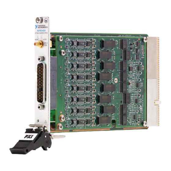
- Page 1 NI PXI-4204 User Manual NI PXI-4204 User Manual June 2007 373529C-01...
- Page 2 Thailand 662 278 6777, Turkey 90 212 279 3031, United Kingdom 44 (0) 1635 523545 For further support information, refer to the Technical Support Information document. To comment on National Instruments documentation, refer to the National Instruments Web site at ni.com/info and enter the info code feedback.
- Page 3 Warranty The NI PXI-4204 is warranted against defects in materials and workmanship for a period of one year from the date of shipment, as evidenced by receipts or other documentation. National Instruments will, at its option, repair or replace equipment that proves to be defective during the warranty period.
- Page 4 Conventions The following conventions are used in this manual: <> Angle brackets that contain numbers separated by an ellipsis represent a range of values associated with a bit or signal name—for example, AO <3..0>. » The » symbol leads you through nested menu items and dialog box options to a final action.
-
Page 5: Table Of Contents
Chapter 1 About the NI PXI-4204 What You Need to Get Started ..................1-2 National Instruments Documentation ................1-2 Installing the Application Software, NI-DAQ, and the DAQ Device ......1-3 Installing the NI PXI-4204 ....................1-3 LED Pattern Descriptions ....................1-4 Chapter 2 Connecting Signals Connecting Signals to the NI PXI-4204 ................2-1... - Page 6 Using a DAQmx Channel Property Node in LabVIEW....3-17 Synchronization and Triggering..............3-19 Synchronizing the NI PXI-4204 ..............3-19 Synchronizing the NI PXI-4204 Using LabVIEW......3-21 Other Application Documentation and Material ............3-22 Calibrating the NI PXI-4204 ..................3-23 Loading Calibration Constants................ 3-23 Self-Calibration ....................
- Page 7 Figure 3-2. Effect of Input Impedance on Signal Measurements ......3-5 Figure 3-3. AI CONV CLK Signal Routing ............3-8 Figure 3-4. NI PXI-4204 PXI Trigger Bus Signal Connection........3-10 Figure 3-5. Typical Program Flowchart..............3-12 Figure 3-6. LabVIEW Channel Property Node with Filtering Enabled at 10 kHz and SS/H Enabled ..............3-18...
-
Page 8: About The Ni Pxi-4204
About the NI PXI-4204 The NI PXI-4204 is part of the PXI-4200 series of data acquisition (DAQ) devices with integrated signal conditioning. The PXI-4200 series reduces measurement setup and configuration complexity by integrating signal conditioning and DAQ on the same product. -
Page 9: What You Need To Get Started
National Instruments Documentation The NI PXI-4204 User Manual is one piece of the documentation set for your DAQ system. You could have any of several types of manuals, depending on the hardware and software in your system. Use the documentation you have as follows: •... -
Page 10: Installing The Application Software, Ni-Daq, And The Daq Device
Refer to the DAQ Getting Started Guide to unpack, install, and configure the NI PXI-4204 in a PXI chassis and then to the SCXI Quick Start Guide if you are using a PXI/SCXI combination chassis. -
Page 11: Led Pattern Descriptions
Chapter 1 About the NI PXI-4204 LED Pattern Descriptions The following LEDs on the NI PXI-4204 front panel confirm the system is functioning properly: • The ACCESS LED is normally green and blinks yellow for a minimum of 100 ms during the NI PXI-4204 configuration. -
Page 12: Connecting Signals
NI PXI-4204. Connecting Signals to the NI PXI-4204 After you have verified that the NI PXI-4204 is installed correctly and self-tested the device, refer to the following sections to connect signals to the device. -
Page 13: Figure 2-1. Installing The Ni Pxi-4204 Device
2 PXI System Controller 5 Injector/Ejector Handle 7 Guides 3 NI PXI-4204 Device Figure 2-1. Installing the NI PXI-4204 Device Caution Refer to the Read Me First: Safety and Radio-Frequency Interference document before removing equipment covers or connecting/disconnecting any signal wires. -
Page 14: Front Signal Connector
16-pin COMBICON connector and one SMB connector. Figure 2-2 shows the pin assignments for the signals. Figure 2-3 shows the front label of the NI PXI-4204, with each set of screw terminals labeled according to the corresponding differential input signal. To connect a... -
Page 15: Figure 2-2. Ni Pxi-4204 Screw Terminals
Chapter 2 Connecting Signals PFI 0/ AI0+ AI0– AI1+ AI1– AI2+ AI2– AI3+ AI3– AI4+ AI4– AI5+ AI5– AI6+ AI6– AI7+ AI7– Figure 2-2. NI PXI-4204 Screw Terminals NI PXI-4204 User Manual ni.com... -
Page 16: Analog Input Connections
The following sections provide a definition of the signal source characteristics, descriptions of various ways to connect signals to the NI PXI-4204, and electrical diagrams showing the signal source and connections. Whenever possible, use shielded twisted-pair field wiring to reduce the effects of unwanted noise sources. -
Page 17: Floating Signal Source Connection
To connect a floating signal source connection to the NI PXI-4204, the signal (V +) is connected to the NI PXI-4204 channel (AIX+). The signal reference (V –) is connected to the channel reference (AIX–). -
Page 18: Shielded Floating Signal Source Connection (Recommended)
Figure 2-5. This is the recommended shielding configuration for floating signal sources. The shielding is grounded at only one point to the NI PXI-4204 chassis ground reference. Connect the signal (V +) to the NI PXI-4204 channel (AIX+). -
Page 19: Ground-Referenced Signal Connection
Note This connection is a characteristic of the signal source and no additional wiring should be added to connect the signal source ground reference to the NI PXI-4204 ground reference. To connect a ground-reference signal source to the NI PXI-4204, the signal +) is connected to the NI PXI-4204 channel (AIX+). -
Page 20: Shielded Ground-Referenced Signal Connection (Recommended)
Figure 2-6. The shielding is grounded at only one point to the signal source ground Ground Reference). Connect the signal (V +) to the NI PXI-4204 channel (AIX+). Connect the signal reference (V –) to the channel reference (AIX–). -
Page 21: Alternative Shielded Ground-Referenced Connection
Figure 2-8 to reduce electrically coupled noise. The shielding is grounded at only one point to the NI PXI-4204 chassis ground reference. Connect the signal (V +) to the NI PXI-4204 channel (AIX+). -
Page 22: High Cmv Connection
NI PXI-4204 chassis ground reference. To connect a signal source with high CMV to the NI PXI-4204, connect the signal (V +) to the NI PXI-4204 channel (AIX+). Connect the signal reference (V –) to the channel reference (AIX–). -
Page 23: Shielded High Cmv Connection
Caution If possible, ground the shielding at the NI PXI-4204, and not at the signal source. Grounding the shielding at the signal source in the presence of a high CMV can create a safety hazard by energizing the shield. - Page 24 Ground AI7+ Reference – AI7– Figure 2-10. Shielded High CMV Connection For more information about the function of the NI PXI-4204 and other measurement considerations, refer to Chapter 3, Using the NI PXI-4204. © National Instruments Corporation 2-13 NI PXI-4204 User Manual...
-
Page 25: Using The Ni Pxi-4204
LabVIEW, and calibration. Theory of Operation Figure 3-1 illustrates the key functional components of the NI PXI-4204, including the DAQ and integrated signal conditioning circuitry. © National Instruments Corporation NI PXI-4204 User Manual... -
Page 26: Block Diagram Of Ni Pxi-4204
Chapter 3 Using the NI PXI-4204 COMBICON Connector Attenuator Attenuator Input/Cal Input/Cal Multiplexer Multiplexer PXI Connector Figure 3-1. Block Diagram of NI PXI-4204 NI PXI-4204 User Manual ni.com... -
Page 27: Signal Conditioning Functional Overview
Using the NI PXI-4204 Signal Conditioning Functional Overview The NI PXI-4204 is part of the NI PXI-4200 series of DAQ devices designed to provide application-specific signal conditioning, DAQ, and integrated field wiring connectivity on the same product. The NI PXI-4204 signal conditioning circuitry is designed to provide attenuation, amplification, filtering, and SS/H capability as described in Table 3-1. -
Page 28: Measurement Considerations
NI PXI-4204 and important factors that can affect your measurement. Differential Signals All of the analog inputs of the NI PXI-4204 are differential. In general, a differential measurement system is preferable because it rejects not only ground loop-induced errors and common-mode voltages, but also the noise picked up in the environment to a certain degree. -
Page 29: Input Impedance
One of the most common sources of common-mode interference is due to 50 or 60 Hz powerline noise. The minimum NI PXI-4204 CMRR is 60 dB. This results in a reduction of CMV by a factor of 1000. The measured signal source impedance can reduce the NI PXI-4204 CMR. -
Page 30: Normal-Mode Rejection
60 Hz signal. In the case of the NI PXI-4204, this specification is 40 db at 60 Hz with a 6 Hz filter setting. This NMR is usually only applicable when taking DC measurements. The NMRR is specified at the powerline frequency because this is typically where most measurement noise arises. -
Page 31: Timing And Control Functional Overview
Using the NI PXI-4204 Timing and Control Functional Overview The NI PXI-4204 is based on the NI E Series DAQ device architecture. This architecture uses the NI data acquisition system timing controller (DAQ-STC) for time-related functions. The DAQ-STC consists of two timing groups that control AI and general-purpose counter/timer functions. -
Page 32: Programmable Function Inputs
(SI2) counter TC. Programmable Function Inputs PFI0 is connected to the front SMB connector of the NI PXI-4204. Software can select PFI0 as the external source for a given timing signal. Any timing signal can use the PFI0 pin as an input, and multiple timing signals can simultaneously use the same PFI. -
Page 33: Device And Pxi Clocks
A/D conversions, digital-to-analog converter (DAC) updates, or general-purpose signals at the I/O connector. The NI PXI-4204 can use either its internal 20 MHz master timebase or a timebase received over the PXI trigger bus on the PXI clock line. This timebase is software configurable. -
Page 34: Table 3-2. Pxi Trigger Bus Timing Signals
PXI Trigger<7> Switch Master Timebase Figure 3-4. NI PXI-4204 PXI Trigger Bus Signal Connection Table 3-2 provides more information about each of the timing signals available on the PXI trigger bus. For more detailed timing signal information, refer to Appendix B, Timing Signal Information. -
Page 35: Developing Your Application
Developing Your Application This section describes the software and programming steps necessary to use the NI PXI-4204. For more information about a particular software or programming process, refer to your ADE documentation. Typical Program Flow Chart Figure 3-5 shows a typical program flow chart for creating an AI voltage channel, taking a measurement, and clearing the data. -
Page 36: Typical Program Flowchart
Chapter 3 Using the NI PXI-4204 Create Task Using DAQ Assistant? Create a Task Programmatically Create Task in DAQ Assistant or MAX Create AI Voltage Channel Hardware Timing/Triggering? Further Configure Channels? Adjust Timing Settings Configure Channels Analyze Data? Process Data... -
Page 37: General Discussion Of Typical Flow Chart
If you are using an ADE other than an NI ADE, or if you want to explicitly create and configure a task for a certain type of acquisition, you can programmatically create the task from your ADE using function or VI calls. -
Page 38: Adjusting Timing And Triggering
Configuring Channel Properties All of the different ADEs used to configure the NI PXI-4204 access an underlying set of NI-DAQmx properties. Table 3-3 lists some of the properties that configure the NI PXI-4204. You can use this list to determine what kinds of properties you need to set to configure the device for your application. -
Page 39: Acquiring, Analyzing, And Presenting
After you acquire the data and perform any required analysis, it is useful to display the data in a graphical form or log it to a file. NI ADEs provide easy-to-use tools for graphical display, such as charts, graphs, slide rules, and gauge indicators. -
Page 40: Developing An Application Using Labview
This section describes in more detail the steps shown in the typical program flowchart in Figure 3-5, such as how to create a task in LabVIEW and configure the channels of the NI PXI-4204. For more information or further instructions, select Help»VI, Function, & How-To Help from the LabVIEW menu bar. -
Page 41: Using A Daqmx Channel Property Node In Labview
DAQmx Clear Task.vi Using a DAQmx Channel Property Node in LabVIEW Note With the NI PXI-4204, you must use property nodes to change filter settings and to enable SS/H. You can use property nodes in LabVIEW to manually configure your channels. - Page 42 Chapter 3 Using the NI PXI-4204 Left-click inside the box labeled Property and select Active Channels. This allows you to specify exactly what channel(s) you want to configure. If you want to configure several channels with different properties, separate the lists of properties with another Active Channels box and assign the appropriate channel to each list of properties.
-
Page 43: Synchronization And Triggering
The NI PXI-4204 that generates the start trigger and the timebase for all of the synchronized devices is called the master. The master NI PXI-4204 exports the shared timing signals through the PXI bus to the slave devices. - Page 44 Chapter 3 Using the NI PXI-4204 Create a Master Task (Optional) Create Master Configure Slave Timing AI Voltage Channels Set Slave to Use Configure Master Timebase from Master Channel Configure Slave Triggering Configure Master Timing Get Master Timebase Source Start Slave Measurement(s)
-
Page 45: Synchronizing The Ni Pxi-4204 Using Labview
Except where otherwise stated, the VIs in Table 3-5 are located on the Functions» All Functions»NI Measurements»DAQmx - Data Acquisition subpalette and accompanying subpalettes in LabVIEW. Table 3-5. Synchronizing the NI PXI-4204 Using LabVIEW Flowchart Step VI or Program Step Create a Master Task (optional) DAQmx Create Task.vi... -
Page 46: Other Application Documentation And Material
• LabVIEW Example Programs, available by selecting Open» Examples from the opening screen. Most of the examples applicable to the NI PXI-4204 are located in Hardware Input and Output» DAQmx»Analog Measurements and Hardware Input and Output»DAQmx»Synchronization»Multi-Device. • PXI-4204 Supported Properties in the LabVIEW VI, Function, &... -
Page 47: Calibrating The Ni Pxi-4204
The digitizer calibration constants are automatically read from the flash memory and loaded into the CalDACs by the NI PXI-4204 hardware the next time the device is powered on. The signal conditioning calibration constants are also read from the flash memory at this time. -
Page 48: External Calibration
DAQmx in LabVIEW. Self Calibrate.vi The results of an internal calibration are stored in the NI PXI-4204 flash memory so that the CalDACs are automatically loaded with the newly calculated calibration constants the next time the NI PXI-4204 is powered on. -
Page 49: Appendix A Specifications
Specifications This appendix lists the specifications for the NI PXI-4204 device. These specifications are typical at 25 °C unless otherwise noted. All specifications are with SS/H disabled unless otherwise noted. Analog Input Number of input channels ...... 8 Input range ..........±100 V Resolution .......... - Page 50 (6 Hz filter setting) .........40 dB Crosstalk at 1 kHz Adjacent channels......–75 dB All other channels......–90 dB FIFO buffer size........512 samples Data transfers ..........DMA, interrupts, programmed I/O DMA modes ...........Scatter-gather (single transfer, demand transfer) Configuration memory size ....512 words NI PXI-4204 User Manual ni.com...
- Page 51 Appendix A Specifications NI PXI-4204 Accuracy Information with SS/H Disabled Absolute Accuracy Absolute Noise + Quantization Accuracy Nominal Range (V) % of Reading (mV) Temp at Full Offset Drift Scale Positive Negative Single (mV) (%/°C) (mV) 24 Hours 1 Year Avg.
- Page 52 .......±50mV typ, ±160 mV max Pre-calibration gain error......±18900 ppm max Signal conditioning component only .......±600 ppm typ, ±1000 ppm max The pre-calibration errors apply only for users doing register level programming. NI-DAQmx users do not see the pre-calibration errors. NI PXI-4204 User Manual ni.com...
- Page 53 Pulse width..........10 ns min Impedance ..........10 kΩ Coupling..........DC PXI Trigger Bus Trigger lines ........... 6 Star trigger..........1, input only PCI Bus Interface Master, slave Power Requirements 1 A at +5 V (±5%) © National Instruments Corporation NI PXI-4204 User Manual...
- Page 54 AI 6 – AI 7 – 21.3 cm (8.39 in.) Figure A-1. NI PXI-4204 Dimensions Weight ............207 g (7.3 oz) Analog input signal connector ....16x1 miniature COMBICON, 3.81 mm pitch Analog input signal mating connector ........16x1 miniature COMBICON screw-terminal connector, 3.81 mm pitch, 28–16 AWG...
- Page 55 Operating temperature......0 to 55 °C Storage temperature ....... –20 to 70 °C Humidity ..........10 to 90% RH, noncondensing Maximum altitude ........2,000 m Pollution Degree (indoor use only) ..2 © National Instruments Corporation NI PXI-4204 User Manual...
- Page 56 Appendix A Specifications Safety The NI PXI-4204 is designed to meet the requirements of the following standards of safety for electrical equipment for measurement, control, and laboratory use: • IEC 61010-1, EN-61010-1 • UL 61010-1, CSA 61010-1 Note For UL and other safety certifications, refer to the product label or visit ni.com/...
-
Page 57: Timing Signal Information
Connecting Timing Signals Caution Exceeding the maximum input voltage ratings listed in Appendix A, Specifications, can damage the device and the computer. NI is not liable for any damage resulting from such signal connections. Programmable Function Input Connections You can externally control seven internal timing signals from PFI0 and the PXI trigger bus pins. - Page 58 Figure B-2. Typical Pretriggered Sequence AI START TRIG Signal The AI START TRIG signal can be input through PFI0, PXI_Trig<0..5>, or PXI Star. The AI START TRIG signal can be output through PFI0 or PXI_Trig<0..5>. NI PXI-4204 User Manual ni.com...
-
Page 59: Ai Start Trig Input Signal Timing
PFI pin is selected as the source of AI START TRIG. Refer to the AI REF TRIG Signal section for a complete description of the use of AI START TRIG and AI REF TRIG in a pretriggered operation. © National Instruments Corporation NI PXI-4204 User Manual... -
Page 60: Ai Ref Trig Input Signal Timing
50 to 100 ns. This output is set to high-impedance at startup. Figures B-5 and B-6 show the input and output timing requirements for AI REF TRIG. Rising-Edge Polarity Falling-Edge Polarity = 10 ns minimum Figure B-5. AI REF TRIG Input Signal Timing NI PXI-4204 User Manual ni.com... - Page 61 AI SAMP CLK is deasserted, t , after the last conversion in the scan is initiated. This output is set to high-impedance at startup. © National Instruments Corporation NI PXI-4204 User Manual...
-
Page 62: Ai Samp Clk Input Signal Timing
AI SAMP CLK. If you use internally generated conversions, the first AI CONV CLK appears when the onboard SI2 counter reaches zero. If you select an external AI CONV CLK, the first external pulse after NI PXI-4204 User Manual ni.com... -
Page 63: Ai Conv Clk Input Signal Timing
50 to 100 ns. This output is set to high-impedance at startup. Figures B-9 and B-10 show the input and output timing requirements for AI CONV CLK. Rising-Edge Polarity Falling-Edge Polarity = 10 ns minimum Figure B-9. AI CONV CLK Input Signal Timing © National Instruments Corporation NI PXI-4204 User Manual... - Page 64 Separate the AI CONV CLK pulses by at least one conversion period. The NI PXI-4204 sample interval counter generates AI CONV CLK unless you select an external source. The AI SAMP CLK signal starts the counter, which counts down and reloads itself until the scan finishes.
- Page 65 Figure B-12 shows the timing for AI HOLD COMPLETE. Note The polarity of AI HOLD COMPLETE is not software selectable when programmed using NI-DAQmx. It is a positive polarity pulse. © National Instruments Corporation NI PXI-4204 User Manual...
- Page 66 Appendix B Timing Signal Information AI CONV CLK AI HOLD COMPLETE = 50 to 100 ns = 400 to 500 ns Figure B-12. AI HOLD COMPLETE Signal Timing NI PXI-4204 User Manual B-10 ni.com...
-
Page 67: Removing The Ni Pxi-4204
Slide the device completely out. The next time you restart the computer the NI PXI-4204 will have a red circle with a white X inside it next to the device in MAX. -
Page 68: Injector/Ejector Handle Position Before Device Removal
MAX: Expand Devices and Interfaces to display the list of installed devices and interfaces. The NI PXI-4204 should have a red circle with a white X inside it next to the device to indicate it has been physically removed from the chassis. -
Page 69: Common Questions
NI PXI-4204 does support digital triggering. Is the NI PXI-4204 an isolated device? No, the NI PXI-4204 is not an isolated device and should not be used in applications with working voltages larger than ±100 V. The NI PXI-4204 has only resistive isolation, which does not fit all definitions for isolation. - Page 70 Appendix D Common Questions When no signal is connected to the NI PXI-4204, what sort of behavior should I expect? While the NI PXI-4204 may react differently due to system and condition variables, in most cases, the resistor divider network will pull the signal to ground and read approximately 0.0 V.
-
Page 71: Glossary
– negative of, or minus ° degree Ω amperes analog-to-digital alternating current analog-to-digital converter—an electronic device, often an integrated circuit, that converts an analog voltage to a digital number application development environment © National Instruments Corporation NI PXI-4204 User Manual... - Page 72 For digital signals, you group channels to form ports. Ports usually consist of either four or eight digital channels. channel clock the clock controlling the time interval between individual channel sampling within a scan. Devices with SS/H do not have this clock. common-mode rejection NI PXI-4204 User Manual ni.com...
- Page 73 Gaussian noise to an analog input signal © National Instruments Corporation NI PXI-4204 User Manual...
- Page 74 Some common example of floating signal sources are batteries, transformers, or thermocouples. grams gain the factor by which a signal is amplified, sometimes expressed in decibels hertz—the number of scans read or updates written per second NI PXI-4204 User Manual ni.com...
- Page 75 R = KS, where R = response, S = stimulus, and K = a constant least significant bit Measurement & Automation Explorer—NI software for configuring devices and channels. © National Instruments Corporation...
- Page 76 National Instruments NI-DAQ NI driver software for DAQ hardware NI-DAQmx the latest NI-DAQ driver with new VIs, functions, and development tools for controlling measurement devices noise an undesirable electrical signal—noise comes from external sources such as the AC power line, motors, generators, transformers, fluorescent lights,...
- Page 77 RTSI bus real-time system integration bus—the NI timing bus that connects DAQ devices directly, for precise synchronization of functions seconds samples samples per second—used to express the rate at which a DAQ device...
- Page 78 Includes both the signal and common-mode voltages. NI PXI-4204 User Manual ni.com...
-
Page 79: Index
3-15 overview (table), 3-11 synchronizing multiple devices, 3-19 AI SAMPLE CLK TIMEBASE signal program flowchart (figure), 3-20 description, B-9 synchronizing the NI PXI-4204, 3-19 overview (table), 3-11 table, 3-21 signal timing (figure), B-9 using LabVIEW, 3-21 AI START TRIG signal... - Page 80 Index AI PAUSE TRIG description, B-8 block diagram of NI PXI-4204, 3-2 overview (table), 3-11 AI REF TRIG description, B-4 input signal timing (figure), B-4 calibration, 3-23 output signal timing (figure), B-5 external calibration, 3-24 overview (table), 3-10 loading calibration constants, 3-23...
- Page 81 2-6 maximum working voltage, A-7 front signal connector, 2-3 Measurement & Automation Explorer (MAX), 1-1 front label of NI PXI-4204 (figure), 2-5 removing NI PXI-4220, C-2 signal assignments (figure), 2-4 measurement considerations, 3-4 steps for signal connection, 2-3 common-mode rejection ratio, 3-5...
- Page 82 (NMR), 3-6 self-calibration, 3-23 shielded floating signal source connection, 2-7 shielded ground-referenced signal connection, 2-9 operation theory. See NI PXI-4204 alternative shielded connection, 2-10 overvoltage protection specifications, A-7 shielded high CMV connection, 2-12 signal conditioning functional blocks (table), 3-3...
- Page 83 Index high CMV connection, 2-11 shielded, 2-12 T/H (Track-and-Hold) circuitry (table), 3-4 front signal connector, 2-1, 2-3 theory of operation See NI PXI-4204 NI PXI-4204, 2-1 timing and control overview, 3-7 signal measurement. See measurement timing and triggering, adjusting, 3-14...
Need help?
Do you have a question about the PXI-4204 and is the answer not in the manual?
Questions and answers