
Subscribe to Our Youtube Channel
Related Manuals for NI PXI-5411


Summary of Contents for NI PXI-5411
- Page 1 NI PXI-6653 User Manual Timing and Synchronization Module for PXI NI PXI-6653 User Manual November 2003 Edition Part Number 370968A-01...
- Page 2 Thailand 662 992 7519, United Kingdom 44 0 1635 523545 For further support information, refer to the Technical Support and Professional Services appendix. To comment on the documentation, send email to techpubs@ni.com. © 2003 National Instruments Corporation. All rights reserved.
- Page 3 Warranty The NI PXI-6653 is warranted against defects in materials and workmanship for a period of one year from the date of shipment, as evidenced by receipts or other documentation. National Instruments will, at its option, repair or replace equipment that proves to be defective during the warranty period.
- Page 4 These classes are known as Class A (for use in industrial-commercial locations only) or Class B (for use in residential or commercial locations). All National Instruments (NI) products are FCC Class A products. Depending on where it is operated, this Class A product could be subject to restrictions in the FCC rules. (In Canada, the Department of Communications (DOC), of Industry Canada, regulates wireless interference in much the same way.) Digital...
-
Page 5: Table Of Contents
Chapter 2 Installing and Configuring Installing the Software ....................2-1 Installing the Hardware....................2-1 Configuring the Module....................2-2 Chapter 3 Hardware Overview NI PXI-6653 Front Panel ....................3-3 Access LED .....................3-4 Active LED......................3-4 Connectors.......................3-5 Hardware Features ......................3-5 Clock Generation ......................3-7 Direct Digital Synthesis (DDS) ...............3-7 PXI_CLK10 and OCXO..................3-8... - Page 6 Calibration Factory Calibration......................4-1 OCXO Frequency ................... 4-1 PXI_CLK10 Phase..................4-1 DDS Start Trigger Phase................. 4-1 DDS Initial Phase.................... 4-2 Additional Information....................4-2 Appendix A Specifications Appendix B Technical Support and Professional Services Glossary Index NI PXI-6653 User Manual ni.com...
-
Page 7: About This Manual
Synchronization Module. The NI PXI-6653 enables you to pass PXI timing and trigger signals between two or more PXI chassis. The NI PXI-6653 can generate and route clock signals between devices in multiple chassis, providing a method to synchronize multiple devices in a multichassis PXI system. -
Page 8: National Instruments Documentation
This phrase refers to the NI PXI-6653 module for the PXI bus. National Instruments Documentation The NI PXI-6653 User Manual is one piece of the documentation set for your measurement system. You could have any of several other documents describing your hardware and software. Use the documentation you have as follows: •... -
Page 9: Introduction
PXI embedded controller or a desktop computer connected to the PXI chassis using MXI-3 hardware If you are using the NI PXI-6653 in a system to synchronize NI PXI-4472, NI PXI-5112, NI PXI-5411, NI PXI-6115, or E Series DAQ modules, you... -
Page 10: Unpacking
Chapter 1 Introduction Unpacking The NI PXI-6653 is shipped in an antistatic package to prevent electrostatic damage to the module. Electrostatic discharge (ESD) can damage several components on the module. Caution Never touch the exposed pins of connectors. To avoid such damage in handling the module, take the following precautions: •... -
Page 11: Safety Information
Avoid contact between your body and the connector block signal when hot swapping modules. Remove power from signal lines before connecting them to or disconnecting them from the product. © National Instruments Corporation NI PXI-6653 User Manual... - Page 12 Working voltage is the highest rms value of an AC or DC voltage that can occur across any particular insulation. MAINS is defined as a hazardous live electrical supply system that powers equipment. Suitably rated measuring circuits may be connected to the MAINS for measuring purposes. NI PXI-6653 User Manual ni.com...
-
Page 13: Installing And Configuring
Examples CD for software installation directions. Note Be sure to install the driver software before installing the NI PXI-6653 hardware. Installing the Hardware The following are general installation instructions. Consult the chassis user manual or technical reference manual for specific instructions and warnings about installing new modules. -
Page 14: Configuring The Module
The two LEDs on the front panel provide information about module status. NI PXI-6653 Front Panel section of Chapter 3, Hardware Overview, describes the LEDs in greater detail. Refer to Figure 3-2, NI PXI-6653 Front Panel, for the parts locator diagram for the NI PXI-6653. NI PXI-6653 User Manual ni.com... -
Page 15: Hardware Overview
Hardware Overview This chapter presents an overview of the hardware functions of the NI PXI-6653. Figure 3-1 provides a functional overview of the NI PXI-6653 hardware. © National Instruments Corporation NI PXI-6653 User Manual... - Page 16 PFI 1 PXI_TRIG<0..7> Comparator Routing PFI<0..1> Threshold Driver/ PFI 2 Comparator Driver/ PFI 3 PCI Interface Comparator Driver/ PFI 4 Comparator Driver/ PFI 5 Comparator PFI<2..5> Threshold Figure 3-1. Functional Overview of the NI PXI-6653 NI PXI-6653 User Manual ni.com...
-
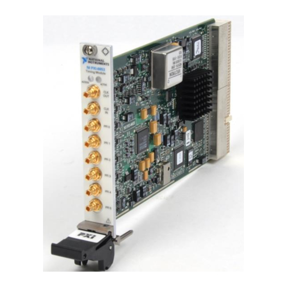
Page 17: Ni Pxi-6653 Front Panel
PFI 1 PFI 2 PFI 3 PFI 4 PFI 5 1 Access LED 4 CLKIN Connector 2 Active LED 5 PFI <0..5> Connectors 3 CLKOUT Connector Figure 3-2. NI PXI-6653 Front Panel © National Instruments Corporation NI PXI-6653 User Manual... -
Page 18: Access Led
Chapter 3 Hardware Overview Access LED The Access LED indicates the communication status of the NI PXI-6653. Refer to Figure 3-2 for the location of the Access LED. Table 3-1 summarizes what the Access LED colors represent. Table 3-1. Access LED Color Indication... -
Page 19: Connectors
NI PXI-6653 front panel. Caution Connections that exceed any of the maximum ratings of input or output signals on the NI PXI-6653 can damage the module and the computer. NI is not liable for any damage resulting from such signal connections. Hardware Features The NI PXI-6653 performs two broad functions: •... - Page 20 Either the OCXO clock or PXI_CLK10 may be routed to this location. DDS Clock This is the output of the NI PXI-6653 DDS. The DDS frequency can be programmed with fine granularity from 1 Hz to 80 MHz. The DDS chip automatically phase-locks to PXI_CLK10.
-
Page 21: Clock Generation
PXI chassis. Clock Generation The NI PXI-6653 can generate two types of clock signals. The first clock is generated using the onboard DDS chip, and the second is generated with a precise 10 MHz oscillator. The following sections describe the two types of clock generation and explain the considerations for choosing either type. -
Page 22: Pxi_Clk10 And Ocxo
This temperature-control scheme minimizes frequency error. An NI PXI-6653 module located in Slot 2 of a PXI chassis can replace the native PXI 10 MHz backplane frequency reference clock (PXI_CLK10) with the more stable and accurate output of the OCXO. All other PXI modules in the chassis that reference the 10 MHz backplane clock benefit from this more accurate frequency reference. -
Page 23: Routing Signals
PXI star triggers, and the PXI/RTSI triggers. The NI PXI-6653 also can route a 10 MHz clock from CLKIN to the PXI 10 MHz reference clock, or it can lock the OCXO to an external reference clock and send that to the PXI 10 MHz reference clock. -
Page 24: Determining Sources And Destinations
Table 3-4 summarizes the sources and destinations of the NI PXI-6653. The destinations are listed in the horizontal heading row, and the sources are listed in the column at the far left. A ✓ in a cell indicates that the source and destination combination defined by that cell is a valid routing combination. -
Page 25: Using Front Panel Pfis As Inputs
Terminating the signals with a 50 Ω resistance is recommended when the source is Note another NI PXI-6653 or any other source with a 50 Ω output. The voltage thresholds for the front-panel PFI inputs are programmable. The input signal is generated by comparing the input voltage on the PFI connectors to the voltage output of software-programmable DACs. -
Page 26: Using Front Panel Pfis As Outputs
The PFI synchronization clock is the same for all routing operations in which Note PFI <0..5> is defined as the output, although the divide-down ratio for this clock (full rate, first divider, second divider) may be chosen on a per route basis. NI PXI-6653 User Manual 3-12 ni.com... -
Page 27: Using The Pxi/Rtsi Triggers
Any of the above signals divided by the second frequency divider , up to 512) Refer to the Choosing the Type of Routing section for more information about the synchronization clock. © National Instruments Corporation 3-13 NI PXI-6653 User Manual... -
Page 28: Using The Pxi Star Triggers
PXI_Trig/PXI_Star synchronization clock. Choosing the Type of Routing The NI PXI-6653 routes signals in one of two ways: asynchronously or synchronously. The following sections describe the two routing types and the considerations for choosing each type. -
Page 29: Synchronous Routing
Some delay is always associated with an asynchronous route, and this delay varies among NI PXI-6653 modules, depending on variations in temperature and chassis voltage. Typical delay times in the NI PXI-6653 for asynchronous routes between various sources and destinations are given in Appendix A, Specifications. - Page 30 If a signal arrives at two chassis within the same clock cycle, each NI PXI-6653 realigns the signal with the synchronization clock and distributes it to the modules in each chassis at the same time.
-
Page 31: Generating A Single Pulse (Global Software Trigger)
NI PXI-6653 includes two clock-divider circuits that can divide the synchronization clock signals by any power of 2 up to 512. Refer to Figures 3-3 and 3-4 for an illustration of how the NI PXI-6653 performs synchronous routing operations. Generating a Single Pulse (Global Software Trigger) The global software trigger is a single pulse with programmable delay that is fired on a software command. -
Page 32: Using The Pxi_Clk10 Pll
PXI_CLK10 to within a few nanoseconds. • The third option is to employ the NI PXI-6653 PLL circuitry for the OCXO. As in option 1, the output of the OCXO replaces the native 10 MHz signal. However, this scheme also requires an input signal on CLKIN. -
Page 33: Calibration
This chapter discusses the calibration of the NI PXI-6653. Calibration consists of verifying the measurement accuracy of a device and correcting for any measurement error. The NI PXI-6653 is factory calibrated before shipment at approximately 25 °C to the levels indicated in Appendix A, Specifications. -
Page 34: Dds Initial Phase
Chapter 4 Calibration DDS Initial Phase The phase of the DDS output is adjusted using this constant so that the DDS outputs from multiple NI PXI-6653 modules are aligned. Additional Information Refer to for additional information on ni.com/calibration NI calibration services. -
Page 35: Appendix A Specifications
Stresses beyond those listed can cause permanent damage to the device. Exposure to absolute maximum rated conditions for extended periods of time can affect device reliability. Functional operation of the device outside the conditions indicated in the operational parts of the specification is not implied. © National Instruments Corporation NI PXI-6653 User Manual... - Page 36 The lower limit is load dependent because of the AC coupling. This limit is less than 1 MHz for high-impedance loads. With an external 50 Ω splitter. This value does not include cable attenuation or splitter insertion loss. NI PXI-6653 User Manual ni.com...
- Page 37 Stresses beyond those listed can cause permanent damage to the device. Exposure to absolute maximum rated conditions for extended periods of time can affect device reliability. Functional operation of the device outside the conditions indicated in the operational parts of the specifications is not implied. Relative to PXI_CLK10. © National Instruments Corporation NI PXI-6653 User Manual...
- Page 38 CtoQ Output-to-output skew, synchronous..500 ps PXI_STAR Trigger Characteristics PXI_STAR <0..12> to PXI_STAR <0..12> output skew at NI PXI-6653 backplane connector ..400 ps Asynchronous delays, t PXI_STAR <0..12> to PFI <0..5> output......7.5 to 13 ns PXI_STAR <0..12> to PXI_TRIG <0..7> output....13 to 19 ns...
- Page 39 Includes temperature stability of OCXO and supporting circuitry. The DDS frequency inherits the relative frequency of PXI_CLK10. For example, if you route the OCXO to PXI_CLK10, the DDS output inherits the same relative frequency accuracy as the OCXO output. © National Instruments Corporation NI PXI-6653 User Manual...
- Page 40 Humidity ..........10 to 95% RH, noncondensing Maximum altitude........2,000 m Pollution Degree (indoor use only) ..2 Safety The NI PXI-6653 meets the requirements of the following standards for safety and electrical equipment for measurement, control, and laboratory use: • IEC 61010-1, EN 61010-1 •...
- Page 41 Refer to the Declaration of Conformity (DoC) for this product for any additional regulatory compliance information. To obtain the DoC for this product, visit , search by model number or product line, and click the ni.com/hardref.nsf appropriate link in the Certification column. © National Instruments Corporation NI PXI-6653 User Manual...
- Page 42 • System Integration—If you have time constraints, limited in-house technical resources, or other project challenges, NI Alliance Program members can help. To learn more, call your local NI office or visit ni.com/alliance • Declaration of Conformity (DoC)—A DoC is our claim of compliance with the Council of the European Communities using the manufacturer’s declaration of conformity.
- Page 43 NI corporate headquarters. Phone numbers for our worldwide offices are listed at the front of this manual. You also can visit the Worldwide Offices section of to access the branch ni.com/niglobal...
- Page 44 Ω accumulator a part where numbers are totaled or stored application development environment asynchronous a property of an event that occurs at an arbitrary time, without synchronization to a reference clock © National Instruments Corporation NI PXI-6653 User Manual...
- Page 45 (2) collecting and measuring the same kinds of electrical signals with A/D and/or DIO devices plugged into a computer, and possibly generating control signals with D/A and/or DIO devices in the same computer NI PXI-6653 User Manual ni.com...
- Page 46 © National Instruments Corporation NI PXI-6653 User Manual...
- Page 47 Intel to replace ISA and EISA. It is achieving widespread acceptance as a standard for PCs and work-stations; it offers a theoretical maximum transfer rate of 132 Mbytes/s Programmable Function Interface NI PXI-6653 User Manual ni.com...
- Page 48 RTSI/PXI triggers or synchronization clock PXI_STAR triggers on an NI PXI-6653 RTSI bus Real-Time System Integration bus—the NI timing bus that connects DAQ devices directly, by means of connectors on top of the devices, for precise synchronization of functions seconds...
- Page 49 CtoQ hold time hold propagation delay time TRIG trigger signal trigger a digital signal that starts or times a hardware event (for example, starting a data acquisition operation) setup time setup volts virtual instrument NI PXI-6653 User Manual ni.com...
- Page 50 (table), 3-6 cable configuration, 3-12 specifications, A-5 calibration certificate (NI resources), B-2 Declaration of Conformity (NI resources), B-1 CE compliance specifications, A-7 destinations, possible destinations (table), 3-11 changing the Active LED color (tip), 3-4 diagnostic tools (NI resources), B-1 CLKIN connector direct digital synthesis.
- Page 51 See also CLKIN connector; CLKOUT category, 1-4 connector; PFI synchronization hardware, 2-1 clock; PFI software, 2-1 connector descriptions, 3-5 instrument drivers (NI resources), B-1 diagram, 3-3 KnowledgeBase, B-1 generating a clock DDS, 3-7 overview, 3-7 PXI_CLK10 and OCXO, 3-8 generating a single pulse (trigger), 3-17...
- Page 52 PXI/RTSI triggers, 3-13 using the PXI_CLK10 PLL, 3-18 power requirement specifications, A-6 programmable function interface. See PFI programming examples (NI resources), B-1 reflections, recommended cable PXI backplane clock, 3-8 configuration, 3-12 PXI star trigger bus. See PXI_STAR <0..12>...
- Page 53 B-1 possible sources (table), 3-11 terminating signals with resistors (note), 3-11 single pulse generation, 3-17 threshold, voltage, 3-11 software (NI resources), B-1 training (NI resources), B-1 software programming choices, overview, 1-2 trigger bus. See PXI_TRIG <0..7> software, installing, 2-1...
Need help?
Do you have a question about the PXI-5411 and is the answer not in the manual?
Questions and answers