
Related Manuals for Renesas SH7203


Summary of Contents for Renesas SH7203
- Page 1 REJ09B0313-0050 SH7203 Group Hardware Manual Renesas 32-Bit RISC Microcomputer SuperH RISC engine Family / SH7200 Series — Preliminary — SH7203 R5S72030W200FP Rev.0.50 Revision Date: May 18, 2006...
- Page 2 Rev. 0.50 May 18, 2006 Page ii of xxx...
- Page 3 (iii) prevention against any malfunction or mishap. Notes regarding these materials 1. These materials are intended as a reference to assist our customers in the selection of the Renesas Technology Corp. product best suited to the customer's application; they do not convey any license under any intellectual property rights, or any other rights, belonging to Renesas Technology Corp.
-
Page 4: General Precautions On Handling Of Product
General Precautions on Handling of Product 1. Treatment of NC Pins Note: Do not connect anything to the NC pins. The NC (not connected) pins are either not connected to any of the internal circuitry or are used as test pins or to reduce noise. If something is connected to the NC pins, the operation of the LSI is not guaranteed. - Page 5 Configuration of This Manual This manual comprises the following items: 1. General Precautions on Handling of Product 2. Configuration of This Manual 3. Preface 4. Contents 5. Overview 6. Description of Functional Modules • CPU and System-Control Modules • On-Chip Peripheral Modules The configuration of the functional description of each module differs according to the module.
-
Page 6: Preface
Preface This LSI is an RISC (Reduced Instruction Set Computer) microcomputer which includes a Renesas Technology-original RISC CPU as its core, and the peripheral functions required to configure a system. Target Users: This manual was written for users who will be using this LSI in the design of application systems. - Page 7 • Description of Numbers and Symbols Aspects of the notations for register names, bit names, numbers, and symbolic names in this manual are explained below. (1) Overall notation In descriptions involving the names of bits and bit fields within this manual, the modules and registers to which the bits belong may be clarified by giving the names in the forms "module name"."register name"."bit name"...
-
Page 8: Contents
• Description of Registers Each register description includes a bit chart, illustrating the arrangement of bits, and a table of bits, describing the meanings of the bit settings. The standard format and notation for bit charts and tables are described below. [Bit Chart] Bit: ... -
Page 9: Table Of Contents
Contents Section 1 Overview....................1 SH7203 Features........................1 Product Lineup........................9 Block Diagram ........................10 Pin Arrangement ........................11 Pin Functions ........................12 Section 2 CPU......................23 Register Configuration......................23 2.1.1 General Registers ....................23 2.1.2 Control Registers ....................24 2.1.3 System Registers..................... 26 2.1.4... - Page 10 Section 3 Floating-Point Unit (FPU)..............69 Features..........................69 Data Formats........................70 3.2.1 Floating-Point Format..................... 70 3.2.2 Non-Numbers (NaN) ....................73 3.2.3 Denormalized Numbers ..................74 Register Descriptions ......................75 3.3.1 Floating-Point Registers ..................75 3.3.2 Floating-Point Status/Control Register (FPSCR)............ 76 3.3.3 Floating-Point Communication Register (FPUL) ...........
- Page 11 5.2.4 Manual Reset ......................108 Address Errors ........................109 5.3.1 Address Error Sources ..................109 5.3.2 Address Error Exception Handling ............... 110 Register Bank Errors......................111 5.4.1 Register Bank Error Sources................. 111 5.4.2 Register Bank Error Exception Handling ............. 111 Interrupts..........................
- Page 12 6.4.2 User Break Interrupt ..................... 139 6.4.3 H-UDI Interrupt ....................139 6.4.4 IRQ Interrupts....................... 139 6.4.5 PINT Interrupts..................... 140 6.4.6 On-Chip Peripheral Module Interrupts ..............141 Interrupt Exception Handling Vector Table and Priority........... 142 Operation ........................... 152 6.6.1 Interrupt Operation Sequence ................152 6.6.2 Stack after Interrupt Exception Handling .............
- Page 13 Usage Notes ........................192 Section 8 Cache....................193 Features..........................193 8.1.1 Cache Structure..................... 193 Register Descriptions ......................196 8.2.1 Cache Control Register 1 (CCR1) ................ 196 8.2.2 Cache Control Register 2 (CCR2) ................ 198 Operation ........................... 202 8.3.1 Searching Cache ....................202 8.3.2 Read Access......................
- Page 14 9.5.2 Normal Space Interface ..................282 9.5.3 Access Wait Control ..................... 287 CSn Assert Period Expansion ................289 9.5.4 9.5.5 MPX-I/O Interface....................290 9.5.6 SDRAM Interface ....................294 9.5.7 Burst ROM (Clocked Asynchronous) Interface............ 338 9.5.8 SRAM Interface with Byte Selection ..............340 9.5.9 PCMCIA Interface....................
- Page 15 11.3.3 Timer I/O Control Register (TIOR) ..............440 11.3.4 Timer Interrupt Enable Register (TIER) ............... 458 11.3.5 Timer Status Register (TSR)................. 461 11.3.6 Timer Buffer Operation Transfer Mode Register (TBTM)........466 11.3.7 Timer Input Capture Control Register (TICCR) ........... 467 11.3.8 Timer Synchronous Clear Register (TSYCR)............
- Page 16 11.4.9 A/D Converter Start Request Delaying Function..........570 11.4.10 TCNT Capture at Crest and/or Trough in Complementary PWM Operation ..574 11.5 Interrupt Sources........................ 575 11.5.1 Interrupt Sources and Priorities ................575 11.5.2 DMAC Activation ....................577 11.5.3 A/D Converter Activation..................577 11.6 Operation Timing.......................
- Page 17 Section 12 Compare Match Timer (CMT)............639 12.1 Features..........................639 12.2 Register Descriptions ......................640 12.2.1 Compare Match Timer Start Register (CMSTR) ..........641 12.2.2 Compare Match Timer Control/Status Register (CMCSR) ........642 12.2.3 Compare Match Counter (CMCNT) ..............644 12.2.4 Compare Match Constant Register (CMCOR) ............. 644 12.3 Operation ...........................
- Page 18 Section 14 Realtime Clock (RTC)..............667 14.1 Features..........................667 14.2 Input/Output Pin ........................ 669 14.3 Register Descriptions ......................670 14.3.1 64-Hz Counter (R64CNT) ..................671 14.3.2 Second Counter (RSECCNT) ................672 14.3.3 Minute Counter (RMINCNT) ................673 14.3.4 Hour Counter (RHRCNT) ..................674 14.3.5 Day of Week Counter (RWKCNT) ..............
- Page 19 15.3.3 Transmit Shift Register (SCTSR) ................. 704 15.3.4 Transmit FIFO Data Register (SCFTDR) ............. 704 15.3.5 Serial Mode Register (SCSMR)................705 15.3.6 Serial Control Register (SCSCR)................708 15.3.7 Serial Status Register (SCFSR)................712 15.3.8 Bit Rate Register (SCBRR) .................. 720 15.3.9 FIFO Control Register (SCFCR) ................
- Page 20 16.4.2 Relationship of Clock Phase, Polarity, and Data ..........783 16.4.3 Relationship between Data Input/Output Pins and Shift Register ......784 16.4.4 Communication Modes and Pin Functions ............786 16.4.5 SSU Mode......................788 16.4.6 SCS Pin Control and Conflict Error..............797 16.4.7 Clock Synchronous Communication Mode ............
- Page 21 18.3.1 Control Register (SSICR) ..................852 18.3.2 Status Register (SSISR) ..................858 18.3.3 Transmit Data Register (SSITDR) ................ 863 18.3.4 Receive Data Register (SSIRDR) ................. 863 18.4 Operation Description ......................864 18.4.1 Bus Format......................864 18.4.2 Non-Compressed Modes..................865 18.4.3 Operation Modes....................875 18.4.4 Transmit Operation ....................
- Page 22 19.9 Usage Notes ........................989 19.9.1 Notes on Port Setting for Multiple Channels Used as Single Channel ....989 Section 20 A/D Converter (ADC) ..............991 20.1 Features..........................991 20.2 Input/Output Pins....................... 993 20.3 Register Descriptions ......................994 20.3.1 A/D Data Registers A to H (ADDRA to ADDRH) ..........995 20.3.2 A/D Control/Status Register (ADCSR) ..............
- Page 23 Section 22 AND/NAND Flash Memory Controller (FLCTL) ......1025 22.1 Features..........................1025 22.2 Input/Output Pins ......................1029 22.3 Register Descriptions ....................... 1030 22.3.1 Common Control Register (FLCMNCR)............1031 22.3.2 Command Control Register (FLCMDCR)............1034 22.3.3 Command Code Register (FLCMCDR).............. 1037 22.3.4 Address Register (FLADR) ................1038 22.3.5 Address Register 2 (FLADR2) ................
- Page 24 23.3.8 FIFO Port Control Registers (CFIFOCTR, D0FIFOCTR, D1FIFOCTR) ..1090 23.3.9 FIFO Port SIE Register (CFIFOSIE) ..............1092 23.3.10 Transaction Counter Registers (D0FIFOTRN, D1FIFOTRN) ......1093 23.3.11 Interrupts Enable Register 0 (INTENB0) ............1094 23.3.12 Interrupt Enabled Register 1 (INTENB1) ............1097 23.3.13 BRDY Interrupts Enable Register (BRDYENB) ..........
- Page 25 Section 24 LCD Controller (LCDC)..............1197 24.1 Features..........................1197 24.2 Input/Output Pins ......................1199 24.3 Register Configuration..................... 1200 24.3.1 LCDC Input Clock Register (LDICKR) ............. 1201 24.3.2 LCDC Module Type Register (LDMTR) ............1203 24.3.3 LCDC Data Format Register (LDDFR) .............. 1206 24.3.4 LCDC Scan Mode Register (LDSMR) ...............
- Page 26 Section 25 Pin Function Controller (PFC) ............1265 25.1 Features..........................1271 25.2 Register Descriptions ....................... 1272 25.2.1 Port B I/O Register L (PBIORL) ................ 1273 25.2.2 Port B Control Registers L1 to L4 (PBCRL1 to PBCRL4) ........ 1274 25.2.3 Port C I/O Register L (PCIORL) ................ 1279 25.2.4 Port C Control Register L1 to L4 (PCCRL1 to PCCRL4) ........
- Page 27 26.7 Port F..........................1348 26.7.1 Register Descriptions ..................1349 26.7.2 Port F Data Registers H and L (PFDRH, PFDRL) ..........1349 26.7.3 Port F Port Registers H and L (PFPRH, PFPRL)..........1353 26.8 Usage Notes ........................1355 Section 27 On-Chip RAM ................1357 27.1 Features..........................
- Page 28 Section 29 User Debugging Interface (H-UDI)..........1399 29.1 Features..........................1399 29.2 Input/Output Pins......................1400 29.3 Register Descriptions ....................... 1401 29.3.1 Bypass Register (SDBPR) .................. 1401 29.3.2 Instruction Register (SDIR) ................1401 29.4 Operation ......................... 1403 29.4.1 TAP Controller ....................1403 29.4.2 Reset Configuration .................... 1404 29.4.3 TDO Output Timing ...................
- Page 29 31.4.15 USB Transceiver Timing ..................1558 31.4.16 LCDC Module Timing..................1560 31.4.17 I/O Port Timing....................1562 31.4.18 H-UDI Related Pin Timing ................. 1563 31.4.19 AC Characteristics Measurement Conditions ............. 1565 31.5 A/D Converter Characteristics ..................1566 31.6 D/A Converter Characteristics ..................1567 Appendix ......................1569 Pin States..........................
- Page 30 Rev. 0.50 May 18, 2006 Page xxx of xxx...
-
Page 31: Section 1 Overview
SH7203 Features This LSI is a single-chip RISC (reduced instruction set computer) microcontroller that includes a Renesas Technology-original RISC CPU as its core, and the peripheral functions required to configure a system. The CPU in this LSI is the SH-2A CPU that provides upward compatibility for SH-1, SH-2, and SH-2E CPUs at object code level. - Page 32 Section 1 Overview Table 1.1 SH7203 Features Items Specification • Renesas Technology original SuperH architecture • Compatible with SH-1, SH-2, and SH-2E at object code level • 32-bit internal data bus • Support of an abundant register-set Sixteen 32-bit general registers ...
- Page 33 Section 1 Overview Items Specification • Floating-point unit Floating-point co-processor included (FPU) • Supports single-precision (32-bit) and double-precision (64-bit) • Supports data type and exceptions that conforms to IEEE754 standard • Two rounding modes: Round to nearest and round to zero •...
- Page 34 Section 1 Overview Items Specification • Bus state controller Address space divided into eight areas (0 to 7), each a maximum of 64 (BSC) Mbytes • The following features settable for each area independently Bus size (8, 16, or 32 bits): Available sizes depend on the area. ...
- Page 35 Section 1 Overview Items Specification • Power-down modes Four power-down modes provided to reduce the power consumption in this LSI Sleep mode Software standby mode Deep standby mode Module standby mode • Multi-function timer Maximum 16 lines of pulse inputs/outputs based on fix channels of 16- pulse unit 2 (MTU2) bit timers •...
- Page 36 Section 1 Overview Items Specification • Serial communication Four channels interface with FIFO • Clocked synchronous or asynchronous mode selectable (SCIF) • Simultaneous transmission and reception (full-duplex communication) supported • Dedicated baud rate generator • Separate 16-byte FIFO registers for transmission and reception •...
- Page 37 Section 1 Overview Items Specification • Direct-connected memory interface with AND-/NAND-type flash AND/NAND flash memory memory controller • (FLCTL) Read/write in sectors • Two types of transfer modes: Command access mode and sector access mode (512-byte data + 16-byte management code: with ECC) •...
- Page 38 Section 1 Overview Items Specification • 64-Kbyte memory for high-speed operation (16 Kbytes × 4) On-chip RAM • 16-Kbyte memory for data retention (4 Kbytes × 4) Power supply voltage • Vcc: 1.1 to 1.3 V • PVcc: 3.0 to 3.6 V •...
-
Page 39: Product Lineup
Section 1 Overview Product Lineup Table 1.2 Product Lineup Product Classification Product Code Package SH7203 R5S72030W200FP QFP3232-240Cu Rev. 0.50 May 18, 2006 Page 9 of 1588 REJ09B0313-0050... -
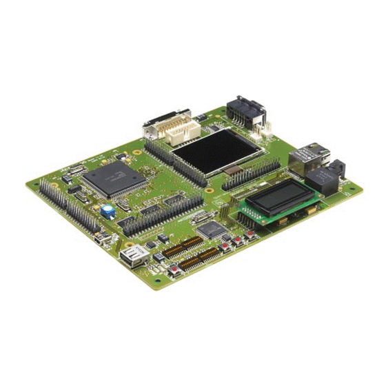
Page 40: Block Diagram
Section 1 Overview Block Diagram SH-2A Floating-point CPU core unit (FPU) CPU instruction fetch bus (F bus) CPU bus (C bus) CPU memory access bus (M bus) (I clock) Instruction Operand On-chip RAM User break Cache UBCTRG output cache memory cache memory (high-speed) controller... -
Page 41: Pin Arrangement
Section 1 Overview Pin Arrangement PB2/SCL1/PINT2/IRQ2 AVss PB3/SDA1/PINT3/IRQ3 PA7/AN7/DA1 PVcc PA6/AN6/DA0 PVcc PA5/AN5 PB4/SCL2/PINT4/IRQ4 AVref PB5/SDA2/PINT5/IRQ5 PA4/AN4 PVss AVcc PA3/AN3 PB6/SCL3/PINT6/IRQ6 PA2/AN2 PB7/SDA3/PINT7/IRQ7 PA1/AN1 PA0/AN0 PD15/D31/PINT7/ADTRG/TIOC4D USBDVss PD14/D30/PINT6/TIOC4C USBDVcc PD13/D29/PINT5/TEND1/TIOC4B USBAPVcc PD12/D28/PINT4/DACK1/TIOC4A USBAPVss PVss REFRIN PD11/D27/PINT3/DREQ1/TIOC3D USBAVss PVcc USBAVcc PD10/D26/PINT2/TEND0/TIOC3C VBUS PD9/D25/PINT1/DACK0/TIOC3B PD8/D24/PINT0/DREQ0/TIOC3A... -
Page 42: Pin Functions
Section 1 Overview Pin Functions Table 1.3 Pin Functions Classification Symbol Name Function Power supply Power supply Power supply pins. All the Vcc pins must be connected to the system power supply. This LSI does not operate correctly if there is a pin left open. - Page 43 Section 1 Overview Classification Symbol Name Function Operating mode Mode set Sets the operating mode. Do not control change the signal level on this pin during operation. MD_CLK1, Clock mode set These pins set the clock operating MD_CLK0 mode. Do not change the signal levels on these pins during operation.
- Page 44 Section 1 Overview Classification Symbol Name Function Interrupts Non-maskable Non-maskable interrupt request pin. interrupt Fix it high when not in use. IRQ7 to IRQ0 Interrupt requests Maskable interrupt request pins. 7 to 0 Level-input or edge-input detection can be selected. When the edge- input detection is selected, the rising edge, falling edge, or both edges can also be selected.
- Page 45 Section 1 Overview Classification Symbol Name Function Bus control Byte select Indicates a write access to bits 15 to 8 of data of external memory or device. Byte select Indicates a write access to bits 23 to 16 of data of external memory or device.
- Page 46 Section 1 Overview Classification Symbol Name Function Direct memory DREQ3 to DMA-transfer Input pins to receive external access controller DREQ0 request requests for DMA transfer. (DMAC) DACK3 to DMA-transfer Output pins for signals indicating DACK0 request accept acceptance of external requests from external devices.
- Page 47 Section 1 Overview Classification Symbol Name Function Realtime clock RTC_X1 Crystal oscillator Connected to 32.768-kHz crystal (RTC) for RTC resonator. RTC_X2 Serial TxD3 to TxD0 Transmit data Data output pins. communication RxD3 to RxD0 Receive data Data input pins. interface with SCK3 to SCK0 Serial clock Clock input/output pins.
- Page 48 Section 1 Overview Classification Symbol Name Function Controller area CTx0, CTx1 CAN bus transmit Output pin for transmit data on the network data CAN bus. (RCAN-TL1) CRx0, CRx1 CAN bus receive Output pin for receive data on the data CAN bus. AND/NAND Flash memory Address latch enable: Asserted for...
- Page 49 Section 1 Overview Classification Symbol Name Function USB2.0 USB D+ data USB bus D+ data. host/function USB D– data USB bus D– data. module (USB) VBUS VBUS input Connected to Vbus on USB bus. REFRIN Reference input Connected to USBAPVss via TBD-kΩ...
- Page 50 Section 1 Overview Classification Symbol Name Function LCD controller LCD_DATA15 to LCD data Data output pin for LCD panel. (LCDC) LCD_DATA0 LCD_CL1 Shift clock LCD shift clock 1/ horizontal sync signal pin. LCD_CL2 Shift clock LCD shift clock 2/dot clock pin. LCD_CLK Clock source LCD clock source input pin.
- Page 51 Section 1 Overview Classification Symbol Name Function User debugging Test clock Test-clock input pin. interface (H-UDI) Test mode select Test-mode select signal input pin. Test data input Serial input pin for instructions and data. Test data output Serial output pin for instructions and data.
- Page 52 Section 1 Overview Rev. 0.50 May 18, 2006 Page 22 of 1588 REJ09B0313-0050...
-
Page 53: Section 2 Cpu
Section 2 CPU Section 2 CPU Register Configuration The register set consists of sixteen 32-bit general registers, four 32-bit control registers, and four 32-bit system registers. 2.1.1 General Registers Figure 2.1 shows the general registers. The sixteen 32-bit general registers are numbered R0 to R15. General registers are used for data processing and address calculation. -
Page 54: Control Registers
Section 2 CPU 2.1.2 Control Registers The control registers consist of four 32-bit registers: the status register (SR), the global base register (GBR), the vector base register (VBR), and the jump table base register (TBR). The status register indicates instruction processing states. The global base register functions as a base address for the GBR indirect addressing mode to transfer data to the registers of on-chip peripheral modules. - Page 55 Section 2 CPU Bit Name Initial Value Description 31 to 15 — All 0 Reserved These bits are always read as 0. The write value should always be 0. BO Bit Indicates that a register bank has overflowed. CS Bit Indicates that, in CLIP instruction execution, the value has exceeded the saturation upper-limit value or fallen below the saturation lower-limit value.
-
Page 56: System Registers
Section 2 CPU 2.1.3 System Registers The system registers consist of four 32-bit registers: the high and low multiply and accumulate registers (MACH and MACL), the procedure register (PR), and the program counter (PC). MACH and MACL store the results of multiply or multiply and accumulate operations. PR stores the return address from a subroutine procedure. -
Page 57: Register Banks
Section 2 CPU 2.1.4 Register Banks For the nineteen 32-bit registers comprising general registers R0 to R14, control register GBR, and system registers MACH, MACL, and PR, high-speed register saving and restoration can be carried out using a register bank. The register contents are automatically saved in the bank after the CPU accepts an interrupt that uses a register bank. -
Page 58: Data Formats
Section 2 CPU Data Formats 2.2.1 Data Format in Registers Register operands are always longwords (32 bits). If the size of memory operand is a byte (8 bits) or a word (16 bits), it is changed into a longword by expanding the sign-part when loaded into a register. -
Page 59: Immediate Data Format
Section 2 CPU 2.2.3 Immediate Data Format Byte (8-bit) immediate data is located in an instruction code. Immediate data accessed by the MOV, ADD, and CMP/EQ instructions is sign-extended and handled in registers as longword data. Immediate data accessed by the TST, AND, OR, and XOR instructions is zero-extended and handled as longword data. -
Page 60: Instruction Features
Section 2 CPU Instruction Features 2.3.1 RISC-Type Instruction Set Instructions are RISC type. This section details their functions. 16-Bit Fixed-Length Instructions Basic instructions have a fixed length of 16 bits, improving program code efficiency. 32-Bit Fixed-Length Instructions The SH-2A additionally features 32-bit fixed-length instructions, improving performance and ease of use. - Page 61 Section 2 CPU Delayed Branch Instructions With the exception of some instructions, unconditional branch instructions, etc., are executed as delayed branch instructions. With a delayed branch instruction, the branch is taken after execution of the instruction immediately following the delayed branch instruction. This reduces disturbance of the pipeline control when a branch is taken.
- Page 62 Section 2 CPU Table 2.4 T Bit SH-2A CPU Description Example of Other CPU T bit is set when R0 ≥ R1. CMP/GE R1,R0 CMP.W R1,R0 The program branches to TRGET0 TRGET0 TRGET0 when R0 ≥ R1 and to TRGET1 TRGET1 TRGET1 when R0 <...
- Page 63 Section 2 CPU (11) Absolute Address When data is accessed by an absolute address, the absolute address value should be placed in the memory table in advance. That value is transferred to the register by loading the immediate data during the execution of the instruction, and the data is accessed in register indirect addressing mode.
-
Page 64: Addressing Modes
Section 2 CPU 2.3.2 Addressing Modes Addressing modes and effective address calculation are as follows: Table 2.8 Addressing Modes and Effective Addresses Addressing Instruction Mode Format Effective Address Calculation Equation Register direct The effective address is register Rn. (The operand —... - Page 65 Section 2 CPU Addressing Instruction Mode Format Effective Address Calculation Equation Register indirect The effective address is the sum of Rn and a 4-bit Byte: @(disp:4, with displacement (disp). The value of disp is zero- Rn + disp displacement extended, and remains unchanged for a byte Word: operation, is doubled for a word operation, and is Rn + disp ×...
- Page 66 Section 2 CPU Addressing Instruction Mode Format Effective Address Calculation Equation Indexed GBR @(R0, GBR) The effective address is the sum of GBR value GBR + R0 indirect and R0. GBR + R0 TBR duplicate The effective address is the sum of TBR value Contents of indirect with and an 8-bit displacement (disp).
- Page 67 Section 2 CPU Addressing Instruction Mode Format Effective Address Calculation Equation PC + disp × 2 PC relative The effective address is the sum of PC value and disp:8 the value that is obtained by doubling the sign- extended 8-bit displacement (disp). disp PC + disp ×...
- Page 68 Section 2 CPU Addressing Instruction Mode Format Effective Address Calculation Equation Immediate The 20-bit immediate data (imm) for the MOVI20 — #imm:20 instruction is sign-extended. Sign- imm (20 bits) extended The 20-bit immediate data (imm) for the MOVI20S — instruction is shifted by eight bits to the left, the upper bits are sign-extended, and the lower bits are padded with zero.
-
Page 69: Instruction Format
Section 2 CPU 2.3.3 Instruction Format The instruction formats and the meaning of source and destination operands are described below. The meaning of the operand depends on the instruction code. The symbols used are as follows: • xxxx: Instruction code •... - Page 70 Section 2 CPU Source Destination Instruction Formats Operand Operand Example m format mmmm: Register Control register or Rm,SR direct system register xxxx xxxx mmmm xxxx mmmm: Register Control register or LDC.L @Rm+,SR indirect with post- system register increment — mmmm: Register indirect mmmm: Register R0 (Register direct) MOV.L @-Rm,R0...
- Page 71 Section 2 CPU Source Destination Instruction Formats Operand Operand Example R0 (Register direct) nnnndddd: nd4 format MOV.B Register indirect R0,@(disp,Rn) with displacement xxxx xxxx nnnn dddd nmd format mmmm: Register nnnndddd: Register MOV.L direct indirect with Rm,@(disp,Rn) displacement xxxx nnnn dddd mmmm mmmmdddd:...
- Page 72 Section 2 CPU Source Destination Instruction Formats Operand Operand Example iiiiiiii: Immediate i format Indexed GBR AND.B indirect #imm,@(R0,GBR) xxxx xxxx iiii iiii iiiiiiii: Immediate R0 (Register direct) #imm,R0 iiiiiiii: Immediate — TRAPA #imm ni format iiiiiiii: Immediate nnnn: Register direct ADD #imm,Rn xxxx nnnn...
-
Page 73: Instruction Set
Section 2 CPU Instruction Set 2.4.1 Instruction Set by Classification Table 2.10 lists the instructions according to their classification. Table 2.10 Classification of Instructions Operation No. of Classification Types Code Function Instructions Data transfer Data transfer Immediate data transfer Peripheral module data transfer Structure data transfer Reverse stack transfer MOVA... - Page 74 Section 2 CPU Operation No. of Classification Types Code Function Instructions Arithmetic Binary addition operations ADDC Binary addition with carry ADDV Binary addition with overflow check CMP/cond Comparison CLIPS Signed saturation value comparison CLIPU Unsigned saturation value comparison Signed division (32 ÷ 32) DIVS Unsigned division (32 ÷...
- Page 75 Section 2 CPU Operation No. of Classification Types Code Function Instructions Logic Logical AND operations Bit inversion Logical OR Memory test and bit set Logical AND and T bit set Exclusive OR Shift ROTL One-bit left rotation ROTR One-bit right rotation ROTCL One-bit left rotation with T bit ROTCR...
- Page 76 Section 2 CPU Operation No. of Classification Types Code Function Instructions System CLRT T bit clear control CLRMAC MAC register clear LDBANK Register restoration from specified register bank entry Load to control register Load to system register No operation RESBANK Register restoration from register bank Return from exception handling SETT T bit set...
- Page 77 Section 2 CPU Operation No. of Classification Types Code Function Instructions Floating-point FSCHG SZ bit inversion instructions FSQRT Floating-point square root FSTS Floating-point store from system register FPUL FSUB Floating-point subtraction FTRC Floating-point conversion with rounding to integer FPU-related Load into floating-point system register Store from floating-point system register instructions BAND...
- Page 78 Section 2 CPU The table below shows the format of instruction codes, operation, and execution states. They are described by using this format according to their classification. Execution Instruction Instruction Code Operation States T Bit Indicated in MSB ↔ Indicated by mnemonic. Indicates summary of Value when no Value of T bit after...
-
Page 79: Data Transfer Instructions
Section 2 CPU 2.4.2 Data Transfer Instructions Table 2.11 Data Transfer Instructions Compatibility Execu- tion SH2, Instruction Instruction Code Operation Cycles T Bit SH2E SH4 SH-2A 1110nnnniiiiiiii imm → sign extension → Rn #imm,Rn 1001nnnndddddddd (disp × 2 + PC) → sign ... - Page 80 Section 2 CPU Compatibility Execu- tion SH2, Instruction Instruction Code Operation Cycles T Bit SH2E SH4 SH-2A 0000nnnnmmmm0110 Rm → (R0 + Rn) MOV.L Rm,@(R0,Rn) 0000nnnnmmmm1100 (R0 + Rm) → MOV.B @(R0,Rm),Rn sign extension → Rn 0000nnnnmmmm1101 (R0 + Rm) → ...
- Page 81 Section 2 CPU Compatibility Execu- tion SH2, Instruction Instruction Code Operation Cycles T Bit SH2E SH4 SH-2A (disp × 4 + Rm) → Rn MOV.L @(disp12,Rm),Rn 0011nnnnmmmm0001 0110dddddddddddd 11000111dddddddd disp × 4 + PC → R0 MOVA @(disp,PC),R0 imm →...
- Page 82 Section 2 CPU Compatibility Execu- tion SH2, Instruction Instruction Code Operation Cycles T Bit SH2E SH4 SH-2A (disp + Rm) → MOVU.B @(disp12,Rm),Rn 0011nnnnmmmm0001 zero extension → Rn 1000dddddddddddd (disp × 2 + Rm) → MOVU.W @(disp12,Rm),Rn 0011nnnnmmmm0001 zero extension →...
-
Page 83: Arithmetic Operation Instructions
Section 2 CPU 2.4.3 Arithmetic Operation Instructions Table 2.12 Arithmetic Operation Instructions Compatibility Execu- tion SH2, Instruction Instruction Code Operation Cycles T Bit SH2E SH4 SH-2A Rn + Rm → Rn Rm,Rn 0011nnnnmmmm1100 Rn + imm → Rn #imm,Rn 0111nnnniiiiiiii Rn + Rm + T →... - Page 84 Section 2 CPU Compatibility Execu- tion SH2, Instruction Instruction Code Operation Cycles T Bit SH2E SH4 SH-2A CLIPS.B When Rn > (H'0000007F), 0100nnnn10010001 (H'0000007F) → Rn, 1 → CS when Rn < (H'FFFFFF80), (H'FFFFFF80) → Rn, 1 → CS ...
- Page 85 Section 2 CPU Compatibility Execu- tion SH2, Instruction Instruction Code Operation Cycles T Bit SH2E SH4 SH-2A EXTU.B Rm,Rn Byte in Rm is 0110nnnnmmmm1100 zero-extended → Rn EXTU.W Rm,Rn Word in Rm is 0110nnnnmmmm1101 zero-extended → Rn Signed operation of (Rn) × ...
-
Page 86: Logic Operation Instructions
Section 2 CPU 2.4.4 Logic Operation Instructions Table 2.13 Logic Operation Instructions Compatibility Execu- tion SH2, Instruction Instruction Code Operation Cycles T Bit SH2E SH4 SH-2A Rn & Rm → Rn 0010nnnnmmmm1001 Rm,Rn R0 & imm → R0 11001001iiiiiiii #imm,R0 (R0 + GBR) &... -
Page 87: Shift Instructions
Section 2 CPU 2.4.5 Shift Instructions Table 2.14 Shift Instructions Compatibility Execu- tion SH2, Instruction Instruction Code Operation Cycles T Bit SH2E SH4 SH-2A T ← Rn ← MSB 0100nnnn00000100 ROTL LSB → Rn → T 0100nnnn00000101 ROTR T ← Rn ← T 0100nnnn00100100 ROTCL T →... -
Page 88: Branch Instructions
Section 2 CPU 2.4.6 Branch Instructions Table 2.15 Branch Instructions Compatibility Execu- tion SH2, SH2E SH4 Instruction Instruction Code Operation Cycles T Bit SH-2A When T = 0, disp × 2 + PC → 10001011dddddddd label 3/1* When T = 1, nop ... -
Page 89: System Control Instructions
Section 2 CPU 2.4.7 System Control Instructions Table 2.16 System Control Instructions Compatibility Execu- tion SH2, SH2E SH4 Instruction Instruction Code Operation Cycles T Bit SH-2A 0 → T 0000000000001000 CLRT 0 → MACH,MACL 0000000000101000 CLRMAC 0100mmmm11100101 LDBANK @Rm,R0 (Specified register bank entry) →... - Page 90 Section 2 CPU Compatibility Execu- tion SH2, Instruction Instruction Code Operation Cycles T Bit SH2E SH4 SH-2A GBR → Rn 0000nnnn00010010 GBR,Rn VBR → Rn 0000nnnn00100010 VBR,Rn Rn-4 → Rn, SR → (Rn) 0100nnnn00000011 STC.L SR,@-Rn Rn-4 → Rn, GBR → (Rn) ...
-
Page 91: Floating-Point Operation Instructions
Section 2 CPU 2.4.8 Floating-Point Operation Instructions Table 2.17 Floating-Point Operation Instructions Compatibility Execu- SH-2A/ tion SH2A- Instruction Instruction Code Operation Cycles T Bit SH2E |FRn| → FRn 1111nnnn01011101 FABS |DRn| → DRn 1111nnn001011101 FABS FRn + FRm → FRn ... - Page 92 Section 2 CPU Compatibility Execu- SH-2A/ tion SH2A- Cycles T Bit Instruction Instruction Code Operation SH2E (R0 + Rm) → FRn 1111nnnnmmmm0110 FMOV.S @(R0, Rm), FRn (R0 + Rm) → DRn 1111nnn0mmmm0110 FMOV.D @(R0, Rm), DRn (Rm) → FRn, Rm+=4 ...
-
Page 93: Fpu-Related Cpu Instructions
Section 2 CPU Compatibility Execu- SH-2A/ tion SH2A- Cycles T Bit Instruction Instruction Code Operation SH2E DRn-DRm → DRn 1111nnn0mmm00001 FSUB DRm, DRn (long)FRm → FPUL 1111mmmm00111101 FTRC FRm, FPUL (long)DRm → FPUL 1111mmm000111101 FTRC DRm, FPUL 2.4.9 FPU-Related CPU Instructions Table 2.18 FPU-Related CPU Instructions... -
Page 94: Bit Manipulation Instructions
Section 2 CPU 2.4.10 Bit Manipulation Instructions Table 2.19 Bit Manipulation Instructions Compatibility Execu- tion SH2, SH2E SH4 SH-2A Instruction Instruction Code Operation Cycles T Bit (imm of (disp + Rn)) & T → 0011nnnn0iii1001 BAND.B #imm3,@(disp12,Rn) Ope- ration 0100dddddddddddd result ~(imm of (disp + Rn)) &... - Page 95 Section 2 CPU Compatibility Execu- tion SH2, Instruction Instruction Code Operation Cycles T Bit SH2E SH4 SH-2A (imm of (disp + Rn)) ^ T → T 0011nnnn0iii1001 BXOR.B #imm3,@(disp12,Rn) Ope- ration 0110dddddddddddd result Rev. 0.50 May 18, 2006 Page 65 of 1588 REJ09B0313-0050...
-
Page 96: Processing States
Section 2 CPU Processing States The CPU has five processing states: reset, exception handling, bus-released, program execution, and power-down. Figure 2.6 shows the transitions between the states. Manual reset from any state Power-on reset from any state Manual reset state Power-on reset state NMI interrupt, IRQ interrupt*,... - Page 97 Section 2 CPU Reset State In the reset state, the CPU is reset. There are two kinds of reset, power-on reset and manual reset. Exception Handling State The exception handling state is a transient state that occurs when exception handling sources such as resets or interrupts alter the CPU’s processing state flow.
- Page 98 Section 2 CPU Rev. 0.50 May 18, 2006 Page 68 of 1588 REJ09B0313-0050...
-
Page 99: Section 3 Floating-Point Unit (Fpu)
Section 3 Floating-Point Unit (FPU) Section 3 Floating-Point Unit (FPU) Features The FPU has the following features. • Conforms to IEEE754 standard • 16 single-precision floating-point registers (can also be referenced as eight double-precision registers) • Two rounding modes: Round to nearest and round to zero •... -
Page 100: Data Formats
Section 3 Floating-Point Unit (FPU) Data Formats 3.2.1 Floating-Point Format A floating-point number consists of the following three fields: • Sign (s) • Exponent (e) • Fraction (f) This LSI can handle single-precision and double-precision floating-point numbers, using the formats shown in figures 3.1 and 3.2. Figure 3.1 Format of Single-Precision Floating-Point Number Figure 3.2 Format of Double-Precision Floating-Point Number The exponent is expressed in biased form, as follows:... - Page 101 Section 3 Floating-Point Unit (FPU) Table 3.1 Floating-Point Number Formats and Parameters Parameter Single-Precision Double-Precision Total bit width 32 bits 64 bits Sign bit 1 bit 1 bit Exponent field 8 bits 11 bits Fraction field 23 bits 52 bits Precision 24 bits 53 bits...
- Page 102 Section 3 Floating-Point Unit (FPU) Table 3.2 shows the ranges of the various numbers in hexadecimal notation. Table 3.2 Floating-Point Ranges Type Single-Precision Double-Precision Signaling non-number H'7FFF FFFF to H'7FC0 0000 H'7FFF FFFF FFFF FFFF to H'7FF8 0000 0000 0000 Quiet non-number H'7FBF FFFF to H'7F80 0001 H'7FF7 FFFF FFFF FFFF to...
-
Page 103: Non-Numbers (Nan)
Section 3 Floating-Point Unit (FPU) 3.2.2 Non-Numbers (NaN) Figure 3.3 shows the bit pattern of a non-number (NaN). A value is NaN in the following case: • Sign bit: Don't care • Exponent field: All bits are 1 • Fraction field: At least one bit is 1 The NaN is a signaling NaN (sNaN) if the MSB of the fraction field is 1, and a quiet NaN (qNaN) if the MSB is 0. -
Page 104: Denormalized Numbers
Section 3 Floating-Point Unit (FPU) 3.2.3 Denormalized Numbers For a denormalized number floating-point value, the exponent field is expressed as 0, and the fraction field as a non-zero value. In the SH2A-FPU, the DN bit in the status register FPSCR is always set to 1, therefore a denormalized number (source operand or operation result) is always flushed to 0 in a floating- point operation that generates a value (an operation other than copy, FNEG, or FABS). -
Page 105: Register Descriptions
Section 3 Floating-Point Unit (FPU) Register Descriptions 3.3.1 Floating-Point Registers Figure 3.4 shows the floating-point register configuration. There are sixteen 32-bit floating-point registers FPR0 to FPR15, referenced by specifying FR0 to FR15, DR0/2/4/6/8/10/12/14. The correspondence between FRPn and the reference name is determined by the PR and SZ bits in FPSCR. -
Page 106: Floating-Point Status/Control Register (Fpscr)
Section 3 Floating-Point Unit (FPU) 3.3.2 Floating-Point Status/Control Register (FPSCR) FPSCR is a 32-bit register that controls floating-point instructions, sets FPU exceptions, and selects the rounding mode. Bit: Cause Initial value: R/W: Bit: Cause Enable Flag Initial value: R/W: Initial Bit Name Value Description... -
Page 107: Floating-Point Communication Register (Fpul)
Section 3 Floating-Point Unit (FPU) Initial Value Bit Name Description FPU Exception Cause Field 17 to 12 Cause All 0 FPU Exception Enable Field 11 to 7 Enable All 0 FPU Exception Flag Field 6 to 2 Flag All 0 When an FPU exception occurs, the bits corresponding to the FPU exception cause field and FPU exception flag field are set to 1. -
Page 108: Rounding
Section 3 Floating-Point Unit (FPU) Rounding In a floating-point instruction, rounding is performed when generating the final operation result from the intermediate result. Therefore, the result of combination instructions such as FMAC will differ from the result when using a basic instruction such as FADD, FSUB, or FMUL. Rounding is performed once in FMAC, but twice in FADD, FSUB, and FMUL. -
Page 109: Floating-Point Exceptions
Section 3 Floating-Point Unit (FPU) Floating-Point Exceptions 3.5.1 FPU Exception Sources The exception sources are as follows: • FPU error (E): When FPSCR.DN = 0 and a denormalized number is input (No error occurs in the SH2A-FPU) • Invalid operation (V): In case of an invalid operation, such as NaN input •... - Page 110 Section 3 Floating-Point Unit (FPU) These possibilities are shown in the individual instruction descriptions. All exception events that originate in the FPU are assigned as the same exception event. The meaning of an exception is determined by software by reading from FPSCR and interpreting the information it contains. If no bits are set in the FPU exception cause field of FPSCR when one or more of bits O, U, I, and V are set in the FPU exception enable field, this indicates that an actual exception source is not generated.
-
Page 111: Section 4 Clock Pulse Generator (Cpg)
Section 4 Clock Pulse Generator (CPG) Section 4 Clock Pulse Generator (CPG) This LSI has a clock pulse generator (CPG) that generates an internal clock (Iφ), a peripheral clock (Pφ), and a bus clock (Bφ). The CPG consists of a crystal oscillator, PLL circuits, and divider circuits. - Page 112 Section 4 Clock Pulse Generator (CPG) Figure 4.1 shows a block diagram of the clock pulse generator. On-chip oscillator Divider 2 × 1 Divider 1 × 1 × 1/2 MTU clock PLL circuit 1 × 1/2 × 1/3 (Iφ, Max. 200 MHz) (×...
- Page 113 Section 4 Clock Pulse Generator (CPG) The clock pulse generator blocks function as follows: Crystal Oscillator The crystal oscillator is an oscillation circuit in which the crystal resonator is connected to the XTAL/EXTAL pin or USB_X1/USB_X2 pin. This can be used according to the clock operating mode.
- Page 114 Section 4 Clock Pulse Generator (CPG) Standby Control Circuit The standby control circuit controls the states of the clock pulse generator and other modules during clock switching, or sleep, software standby or deep standby mode. In addition, the standby control register is provided to control the power-down mode of other modules.
-
Page 115: Input/Output Pins
Section 4 Clock Pulse Generator (CPG) Input/Output Pins Table 4.1 lists the clock pulse generator pins and their functions. Table 4.1 Pin Configuration and Functions of the Clock Pulse Generator Function Function Function (Clock Operating (Clock Operating (Clock Operating Pin Name Symbol Mode 0,1) Mode 2) -
Page 116: Clock Operating Modes
Section 4 Clock Pulse Generator (CPG) Clock Operating Modes Table 4.2 shows the relationship between the combinations of the mode control pins (MD_CLK1 and MD_CLK0) and the clock operating modes. Table 4.3 shows the usable frequency ranges in the clock operating modes. Table 4.2 Clock Operating Modes Pin Values... - Page 117 Section 4 Clock Pulse Generator (CPG) • Mode 2 In mode 2, the CKIO pin functions as an input pin and draws an external clock signal. The PLL circuit shapes waveform and the frequency is multiplied according to the frequency control register setting before the clock is supplied to the LSI.
- Page 118 Section 4 Clock Pulse Generator (CPG) Table 4.3 Relationship between Clock Operating Mode and Frequency Range Frequency Ratio of Selectable Frequency Range (MHz) Multiplier Clock Internal Clock Frequencies Operating FRQCR Output Clock Internal Clock Peripheral Mode Setting* Circuit (I:B:P)* (CKIO Pin) (Iφ) Clock (Pφ) Input Clock*...
- Page 119 Section 4 Clock Pulse Generator (CPG) Frequency Ratio of Selectable Frequency Range (MHz) Multiplier Clock Internal Clock Frequencies Operating FRQCR Output Clock Internal Clock Peripheral Mode Setting* Circuit (I:B:P)* (CKIO Pin) (Iφ) Clock (Pφ) Input Clock* Bus Clock (Bφ) H'x206 ON (×...
- Page 120 Section 4 Clock Pulse Generator (CPG) 2. The frequency of the peripheral clock is as follows: the frequency on the EXTAL pin × the frequency-multiplier of the PLL In mode 0 circuit × the divisor of the divider 1 (the frequency on the EXTAL pin × 1/2) × the frequency-multiplier of In mode 1 the PLL circuit ×...
-
Page 121: Register Descriptions
Section 4 Clock Pulse Generator (CPG) Register Descriptions The clock pulse generator has the following registers. Table 4.4 Register Configuration Register Name Abbreviation R/W Initial Value Address Access Size Frequency control register FRQCR H'0003 H'FFFE0010 16 4.4.1 Frequency Control Register (FRQCR) FRQCR is a 16-bit readable/writable register used to specify whether a clock is output from the CKIO pin during normal operation mode, release of bus mastership, software standby mode and standby mode cancellation. - Page 122 Section 4 Clock Pulse Generator (CPG) Initial Bit Name Value Description 13, 12 CKOEN[1:0] 00 Clock Output Enable Specifies the CKIO pin outputs clock signals, or is set to a fixed level or high impedance (Hi-Z) during normal operation mode, release of bus mastership, standby mode, or cancellation of standby mode.
- Page 123 Section 4 Clock Pulse Generator (CPG) Initial Value Bit Name Description 7 to 5 All 0 Reserved These bits are always read as 0. The write value should always be 0. Internal Clock Frequency Division Ratio This bit specifies the frequency division ratio of the internal clock with respect to the output frequency of PLL circuit.
-
Page 124: Changing The Frequency
Section 4 Clock Pulse Generator (CPG) Changing the Frequency The frequency of the internal clock (Iφ) and peripheral clock (Pφ) can be changed either by changing the multiplication rate of PLL circuit or by changing the division rates of divider. All of these are controlled by software through the frequency control register (FRQCR). -
Page 125: Changing The Division Ratio
Section 4 Clock Pulse Generator (CPG) 4.5.2 Changing the Division Ratio Counting by the WDT does not proceed if the frequency divisor is changed but the multiplier is not. 1. In the initial state, IFC = B'0 and PFC[2:0] = B'011. 2. -
Page 126: Notes On Board Design
Section 4 Clock Pulse Generator (CPG) Notes on Board Design 4.6.1 Note on Inputting External Clock Figure 4.2 is an example of connecting the external clock input. When putting the XTAL pin in open state, make sure the parasitic capacitance is less than or equal to 10 pF. To stably input the external clock with enough PLL stabilizing time at power on or releasing the standby, wait longer than the oscillation stabilizing time. -
Page 127: Note On Resonator
Section 4 Clock Pulse Generator (CPG) 4.6.3 Note on Resonator Since various characteristics related to the resonator are closely linked to the user’s board design, thorough evaluation is necessary on the user’s part, using the resonator connection examples shown in this section as a guide. As the parameters for the oscillation circuit will depend on the floating capacitance of the resonator and the user board, the parameters should be determined in consultation with the resonator manufacturer. - Page 128 Section 4 Clock Pulse Generator (CPG) Rev. 0.50 May 18, 2006 Page 98 of 1588 REJ09B0313-0050...
-
Page 129: Section 5 Exception Handling
Section 5 Exception Handling Section 5 Exception Handling Overview 5.1.1 Types of Exception Handling and Priority Exception handling is started by sources, such as resets, address errors, register bank errors, interrupts, and instructions. Table 5.1 shows their priorities. When several exception handling sources occur at once, they are processed according to the priority shown. - Page 130 Section 5 Exception Handling Type Exception Handling Priority Interrupt On-chip peripheral modules C bus interface 3 (IIC3) High Serial communications interface with FIFO (SCIF) Synchronous serial communications unit (SSU) Serial sound interface (SSI) AND/NAND flash memory controller (FLCTL) Realtime clock (RTC) Controller area network (RCAN-TL1) Instruction Trap instruction (TRAPA instruction)
-
Page 131: Exception Handling Operations
Section 5 Exception Handling 5.1.2 Exception Handling Operations The exception handling sources are detected and start processing according to the timing shown in table 5.2. Table 5.2 Timing of Exception Source Detection and Start of Exception Handling Exception Source Timing of Source Detection and Start of Handling Starts when the RES pin changes from low to high, when the Reset Power-on reset... - Page 132 Section 5 Exception Handling Exception Source Timing of Source Detection and Start of Handling Instructions Floating point Starts when detecting invalid operation exception defined by operation IEEE standard 754, division-by-zero exception, overflow, instructions underflow, or inexact exception. Also starts when qNaN or ±∞ is input to the source for a floating point operation instruction when the QIS bit in FPSCR is set.
-
Page 133: Exception Handling Vector Table
Section 5 Exception Handling 5.1.3 Exception Handling Vector Table Before exception handling begins running, the exception handling vector table must be set in memory. The exception handling vector table stores the start addresses of exception service routines. (The reset exception handling table holds the initial values of PC and SP.) All exception sources are given different vector numbers and vector table address offsets, from which the vector table addresses are calculated. - Page 134 Section 5 Exception Handling Vector Exception Sources Numbers Vector Table Address Offset Integer division exception H'00000044 to H'00000047 (division by zero) Integer division exception (overflow) H'00000048 to H'0000004B (Reserved by system) H'0000004C to H'0000004F H'0000007C to H'0000007F Trap instruction (user vector) H'00000080 to H'00000083 H'000000FC to H'000000FF External interrupts (IRQ, PINT),...
-
Page 135: Resets
Section 5 Exception Handling Resets 5.2.1 Input/Output Pins Table 5.5 shows the reset-related pin configuration. Table 5.5 Pin Configuration Pin Name Symbol Function Power-on reset Input When this pin is driven low, this LSI shifts to the power- on reset processing MRES Manual reset Input... -
Page 136: Power-On Reset
Section 5 Exception Handling 5.2.3 Power-On Reset Power-On Reset by Means of RES Pin When the RES pin is driven low, this LSI enters the power-on reset state. To reliably reset this LSI, the RES pin should be kept at the low level for the duration of the oscillation settling time at power-on or when in software standby mode (when the clock is halted), or at least 20-tcyc (unfixed) when the clock is running. - Page 137 Section 5 Exception Handling Power-On Reset Initiated by WDT When a setting is made for a power-on reset to be generated in the WDT’s watchdog timer mode, and WTCNT of the WDT overflows, this LSI enters the power-on reset state. In this case, WRCSR of the WDT and FRQCR of the CPG are not initialized by the reset signal generated by the WDT.
-
Page 138: Manual Reset
Section 5 Exception Handling 5.2.4 Manual Reset Manual Reset by Means of MRES Pin When the MRES pin is driven low, this LSI enters the manual reset state. To reset this LSI without fail, the MRES pin should be kept at the low level for at least 20-tcyc. In the manual reset state, the CPU’s internal state is initialized, but all the on-chip peripheral module registers are not initialized. -
Page 139: Address Errors
Section 5 Exception Handling Address Errors 5.3.1 Address Error Sources Address errors occur when instructions are fetched or data read or written, as shown in table 5.7. Table 5.7 Bus Cycles and Address Errors Bus Cycle Type Master Bus Cycle Description Address Errors Instruction Instruction fetched from even address... -
Page 140: Address Error Exception Handling
Section 5 Exception Handling 5.3.2 Address Error Exception Handling When an address error occurs, the bus cycle in which the address error occurred ends. When the executing instruction then finishes, address error exception handling starts. The CPU operates as follows: 1. -
Page 141: Register Bank Errors
Section 5 Exception Handling Register Bank Errors 5.4.1 Register Bank Error Sources Bank Overflow In the state where saving has already been performed to all register bank areas, bank overflow occurs when acceptance of register bank overflow exception has been set by the interrupt controller (the BOVE bit in IBNR of the INTC is set to 1) and an interrupt that uses a register bank has occurred and been accepted by the CPU. -
Page 142: Interrupts
Section 5 Exception Handling Interrupts 5.5.1 Interrupt Sources Table 5.8 shows the sources that start interrupt exception handling. These are divided into NMI, user breaks, H-UDI, IRQ, PINT, and on-chip peripheral modules. Table 5.8 Interrupt Sources Number of Type Request Source Sources NMI pin (external input) User break... -
Page 143: Interrupt Priority Level
Section 5 Exception Handling 5.5.2 Interrupt Priority Level The interrupt priority order is predetermined. When multiple interrupts occur simultaneously (overlap), the interrupt controller (INTC) determines their relative priorities and starts processing according to the results. The priority order of interrupts is expressed as priority levels 0 to 16, with priority 0 the lowest and priority 16 the highest. -
Page 144: Interrupt Exception Handling
Section 5 Exception Handling 5.5.3 Interrupt Exception Handling When an interrupt occurs, its priority level is ascertained by the interrupt controller (INTC). NMI is always accepted, but other interrupts are only accepted if they have a priority level higher than the priority level set in the interrupt mask level bits (I3 to I0) of the status register (SR). -
Page 145: Exceptions Triggered By Instructions
Section 5 Exception Handling Exceptions Triggered by Instructions 5.6.1 Types of Exceptions Triggered by Instructions Exception handling can be triggered by trap instructions, general illegal instructions, slot illegal instructions, and integer division exceptions, as shown in table 5.10. Table 5.10 Types of Exceptions Triggered by Instructions Type Source Instruction Comment... -
Page 146: Trap Instructions
Section 5 Exception Handling 5.6.2 Trap Instructions When a TRAPA instruction is executed, trap instruction exception handling starts. The CPU operates as follows: 1. The exception service routine start address which corresponds to the vector number specified in the TRAPA instruction is fetched from the exception handling vector table. 2. -
Page 147: General Illegal Instructions
Section 5 Exception Handling 5.6.4 General Illegal Instructions When an undefined code, including FPU instructions and FPU-related CPU instructions in FPU module standby state, placed anywhere other than immediately after a delayed branch instruction, i.e., in a delay slot, is decoded, general illegal instruction exception handling starts. When the FPU has entered a module standby state, the floating point instruction and FPU-related CPU instructions are handled as undefined codes. -
Page 148: Floating Point Operation Instructions
Section 5 Exception Handling 5.6.6 Floating Point Operation Instructions An FPU exception is generated when the V, Z, O, U or I bit in the FPU enable field (Enable) of the floating point status/control register (FPSCR) is set. This indicates the occurrence of an invalid operation exception defined by the IEEE standard 754, a division-by-zero exception, overflow (in the case of an instruction for which this is possible), underflow (in the case of an instruction for which this is possible), or inexact exception (in the case of an instruction for which this is... -
Page 149: When Exception Sources Are Not Accepted
Section 5 Exception Handling When Exception Sources Are Not Accepted When an address error, FPU exception, register bank error (overflow), or interrupt is generated immediately after a delayed branch instruction, it is sometimes not accepted immediately but stored instead, as shown in table 5.11. When this happens, it will be accepted when an instruction that can accept the exception is decoded. -
Page 150: Stack Status After Exception Handling Ends
Section 5 Exception Handling Stack Status after Exception Handling Ends The status of the stack after exception handling ends is as shown in table 5.12. Table 5.12 Stack Status After Exception Handling Ends Exception Type Stack Status Address error Address of instruction 32 bits after executed instruction 32 bits... - Page 151 Section 5 Exception Handling Exception Type Stack Status General illegal instruction Start address of general 32 bits illegal instruction 32 bits Integer division instruction Start address of relevant 32 bits integer division instruction 32 bits FPU exception Address of instruction 32 bits after executed instruction 32 bits...
-
Page 152: Usage Notes
Section 5 Exception Handling Usage Notes 5.9.1 Value of Stack Pointer (SP) The value of the stack pointer must always be a multiple of four. If it is not, an address error will occur when the stack is accessed during exception handling. 5.9.2 Value of Vector Base Register (VBR) The value of the vector base register must always be a multiple of four. -
Page 153: Section 6 Interrupt Controller (Intc)
Section 6 Interrupt Controller (INTC) Section 6 Interrupt Controller (INTC) The interrupt controller (INTC) ascertains the priority of interrupt sources and controls interrupt requests to the CPU. The INTC registers set the order of priority of each interrupt, allowing the user to process interrupt requests according to the user-set priority. - Page 154 Section 6 Interrupt Controller (INTC) Figure 6.1 shows a block diagram of the INTC. IRQOUT IRQ7 to IRQ0 Input control PINT7 to PINT0 (Interrupt request) (Interrupt request) H-UDI Interrupt (Interrupt request) DMAC request Com- (Interrupt request) parator (Interrupt request) LCDC (Interrupt request) (Interrupt request) I3 I2 I1 I0...
-
Page 155: Input/Output Pins
Section 6 Interrupt Controller (INTC) Input/Output Pins Table 6.1 shows the pin configuration of the INTC. Table 6.1 Pin Configuration Pin Name Symbol Function Nonmaskable interrupt input Input Input of nonmaskable interrupt request signal Interrupt request input pins IRQ7 to IRQ0 Input Input of maskable interrupt request signals... -
Page 156: Register Descriptions
Section 6 Interrupt Controller (INTC) Register Descriptions The INTC has the following registers. These registers are used to set the interrupt priorities and control detection of the external interrupt input signal. Table 6.2 Register Configuration Initial Access Register Name Abbreviation R/W Value Address Size... -
Page 157: Interrupt Priority Registers 01, 02, 05 To 17 (Ipr01, Ipr02, Ipr05 To Ipr17)
Section 6 Interrupt Controller (INTC) 6.3.1 Interrupt Priority Registers 01, 02, 05 to 17 (IPR01, IPR02, IPR05 to IPR17) IPR01, IPR02, and IPR05 to IPR17 are 16-bit readable/writable registers in which priority levels from 0 to 15 are set for IRQ interrupts, PINT interrupts, and on-chip peripheral module interrupts. Table 6.3 shows the correspondence between the interrupt request sources and the bits in IPR01, IPR02, and IPR05 to IPR17. - Page 158 Section 6 Interrupt Controller (INTC) Register Name Bits 15 to 12 Bits 11 to 8 Bits 7 to 4 Bits 3 to 0 Interrupt priority IIC3-3 SCIF0 SCIF1 SCIF2 register 13 Interrupt priority SCIF3 SSU0 SSU1 SSI0 register 14 Interrupt priority SSI1 SSI2 SSI3...
-
Page 159: Interrupt Control Register 0 (Icr0)
Section 6 Interrupt Controller (INTC) 6.3.2 Interrupt Control Register 0 (ICR0) ICR0 is a 16-bit register that sets the input signal detection mode for the external interrupt input pin NMI, and indicates the input level at the NMI pin. Bit: NMIL NMIE Initial value:... -
Page 160: Interrupt Control Register 1 (Icr1)
Section 6 Interrupt Controller (INTC) 6.3.3 Interrupt Control Register 1 (ICR1) ICR1 is a 16-bit register that specifies the detection mode for external interrupt input pins IRQ7 to IRQ0 individually: low level, falling edge, rising edge, or both edges. Bit: IRQ71S IRQ70S IRQ61S IRQ60S IRQ51S IRQ50S IRQ41S IRQ40S IRQ31S IRQ30S IRQ21S IRQ20S IRQ11S IRQ10S IRQ01S IRQ00S Initial value: R/W:... -
Page 161: Interrupt Control Register 2 (Icr2)
Section 6 Interrupt Controller (INTC) 6.3.4 Interrupt Control Register 2 (ICR2) ICR2 is a 16-bit register that specifies the detection mode for external interrupt input pins PINT7 to PINT0 individually: low level or high level. Bit: PINT7S PINT6S PINT5S PINT4S PINT3S PINT2S PINT1S PINT0S Initial value: R/W: Initial... -
Page 162: Irq Interrupt Request Register (Irqrr)
Section 6 Interrupt Controller (INTC) 6.3.5 IRQ Interrupt Request Register (IRQRR) IRQRR is a 16-bit register that indicates interrupt requests from external input pins IRQ7 to IRQ0. If edge detection is set for the IRQ7 to IRQ0 interrupts, writing 0 to the IRQ7F to IRQ0F bits after reading IRQ7F to IRQ0F = 1 cancels the retained interrupts. - Page 163 Section 6 Interrupt Controller (INTC) Initial Value Bit Name Description IRQ Interrupt Request IRQ7F R/(W)* These bits indicate the status of the IRQ7 to IRQ0 IRQ6F R/(W)* interrupt requests. IRQ5F R/(W)* Level detection: IRQ4F R/(W)* 0: IRQn interrupt request has not occurred [Clearing condition] IRQ3F R/(W)*...
-
Page 164: Pint Interrupt Enable Register (Pinter)
Section 6 Interrupt Controller (INTC) 6.3.6 PINT Interrupt Enable Register (PINTER) PINTER is a 16-bit register that enables interrupt request inputs to external interrupt input pins PINT7 to PINT0. Bit: PINT7E PINT6E PINT5E PINT4E PINT3E PINT2E PINT1E PINT0E Initial value: R/W: Initial Bit Name... -
Page 165: Pint Interrupt Request Register (Pirr)
Section 6 Interrupt Controller (INTC) 6.3.7 PINT Interrupt Request Register (PIRR) PIRR is a 16-bit register that indicates interrupt requests from external input pins PINT7 to PINT0. Bit: PINT7R PINT6R PINT5R PINT4R PINT3R PINT2R PINT1R PINT0R Initial value: R/W: Initial Bit Name Value Description... -
Page 166: Bank Control Register (Ibcr)
Section 6 Interrupt Controller (INTC) 6.3.8 Bank Control Register (IBCR) IBCR is a 16-bit register that enables or disables use of register banks for each interrupt priority level. Bit: Initial value: R/W: Initial Bit Name Value Description Enable These bits enable or disable use of register banks for interrupt priority levels 15 to 1. -
Page 167: Bank Number Register (Ibnr)
Section 6 Interrupt Controller (INTC) 6.3.9 Bank Number Register (IBNR) IBNR is a 16-bit register that enables or disables use of register banks and register bank overflow exception. IBNR also indicates the bank number to which saving is performed next through the bits BN3 to BN0. - Page 168 Section 6 Interrupt Controller (INTC) Initial Value Bit Name Description 3 to 0 BN[3:0] 0000 Bank Number These bits indicate the bank number to which saving is performed next. When an interrupt using register banks is accepted, saving is performed to the register bank indicated by these bits, and BN is incremented by 1.
-
Page 169: Interrupt Sources
Section 6 Interrupt Controller (INTC) Interrupt Sources There are six types of interrupt sources: NMI, user break, H-UDI, IRQ, PINT, and on-chip peripheral modules. Each interrupt has a priority level (0 to 16), with 0 the lowest and 16 the highest. -
Page 170: Pint Interrupts
Section 6 Interrupt Controller (INTC) checked by reading the IRQ interrupt request bits (IRQ7F to IRQ0F) in the IRQ interrupt request register (IRQRR). When using edge-sensing for IRQ interrupts, an interrupt request is detected due to change of the IRQ7 to IRQ0 pin states, and an interrupt request signal is sent to the INTC. The result of IRQ interrupt request detection is retained until that interrupt request is accepted. -
Page 171: On-Chip Peripheral Module Interrupts
Section 6 Interrupt Controller (INTC) 6.4.6 On-Chip Peripheral Module Interrupts On-chip peripheral module interrupts are generated by the following on-chip peripheral modules: • Direct memory access controller (DMAC) • USB2.0 host/function module (USB) • LCD controller (LCDC) • Compare match timer (CMT) •... -
Page 172: Interrupt Exception Handling Vector Table And Priority
Section 6 Interrupt Controller (INTC) Interrupt Exception Handling Vector Table and Priority Table 6.4 lists interrupt sources and their vector numbers, vector table address offsets, and interrupt priorities. Each interrupt source is allocated a different vector number and vector table address offset. Vector table addresses are calculated from the vector numbers and vector table address offsets. - Page 173 Section 6 Interrupt Controller (INTC) Table 6.4 Interrupt Exception Handling Vectors and Priorities Interrupt Vector Setting Interrupt Unit Vector Table Priority Corresponding Internal Default (Initial Value) Interrupt Source Vector Address Offset IPR (Bit) Priority Priority H'0000002C to High H'0000002F ...
- Page 174 Section 6 Interrupt Controller (INTC) Interrupt Vector Setting Interrupt Unit Vector Table Priority Corresponding Internal Default (Initial Value) Interrupt Source Vector Address Offset IPR (Bit) Priority Priority PINT PINT5 H'00000154 to 0 to 15 (0) IPR05 (15 to 12) High H'00000157 PINT6 H'00000158 to...
- Page 175 Section 6 Interrupt Controller (INTC) Interrupt Vector Setting Interrupt Unit Vector Table Priority Corresponding Internal Default (Initial Value) Interrupt Source Vector Address Offset IPR (Bit) Priority Priority DMAC DMAC7 DEI7 H'00000220 to 0 to 15 (0) IPR07 (3 to 0) High H'00000223 HEI7...
- Page 176 Section 6 Interrupt Controller (INTC) Interrupt Vector Setting Interrupt Unit Vector Table Priority Corresponding Internal Default (Initial Value) Interrupt Source Vector Address Offset IPR (Bit) Priority Priority MTU2 MTU1 TGI1A H'00000264 to 0 to 15 (0) IPR10 (15 to 12) High H'00000267 TGI1B...
- Page 177 Section 6 Interrupt Controller (INTC) Interrupt Vector Setting Interrupt Unit Vector Table Priority Corresponding Internal Default (Initial Value) Interrupt Source Vector Address Offset IPR (Bit) Priority Priority MTU2 MTU4 TGI4A H'00000298 to 0 to 15 (0) IPR11 (7 to 4) High H'0000029B TGI4B...
- Page 178 Section 6 Interrupt Controller (INTC) Interrupt Vector Setting Interrupt Unit Vector Table Priority Corresponding Internal Default (Initial Value) Interrupt Source Vector Address Offset IPR (Bit) Priority Priority IIC3 IIC3-2 STPI2 H'000002D8 to 0 to 15 (0) IPR12 (3 to 0) High H'000002DB NAKI2...
- Page 179 Section 6 Interrupt Controller (INTC) Interrupt Vector Setting Interrupt Unit Vector Table Priority Corresponding Internal Default (Initial Value) Interrupt Source Vector Address Offset IPR (Bit) Priority Priority SCIF SCIF1 BRI1 H'00000310 to IPR13 (7 to 4) High 0 to 15 (0) H'00000313 ERI1 H'00000314 to...
- Page 180 Section 6 Interrupt Controller (INTC) Interrupt Vector Setting Interrupt Unit Vector Table Priority Corresponding Internal Default (Initial Value) Interrupt Source Vector Address Offset IPR (Bit) Priority Priority SSU1 SSERI1 211 H'0000034C to IPR14 (7 to 4) High 0 to 15 (0) H'0000034F SSRXI1 212 H'00000350 to...
- Page 181 Section 6 Interrupt Controller (INTC) Interrupt Vector Setting Interrupt Unit Vector Table Priority Corresponding Internal Default (Initial Value) Interrupt Source Vector Address Offset IPR (Bit) Priority Priority RCAN- RCAN0 ERS0 H'000003A8 to 0 to 15 (0) IPR16 (3 to 0) High H'000003AB OVR0...
-
Page 182: Operation
Section 6 Interrupt Controller (INTC) Operation 6.6.1 Interrupt Operation Sequence The sequence of interrupt operations is described below. Figure 6.2 shows the operation flow. 1. The interrupt request sources send interrupt request signals to the interrupt controller. 2. The interrupt controller selects the highest-priority interrupt from the interrupt requests sent, following the priority levels set in interrupt priority registers 01, 02, and 05 to 17 (IPR01, IPR02, and IPR05 to IPR17). - Page 183 Section 6 Interrupt Controller (INTC) Notes: The interrupt source flag should be cleared in the interrupt handler. After clearing the interrupt source flag, "time from occurrence of interrupt request until interrupt controller identifies priority, compares it with mask bits in SR, and sends interrupt request signal to CPU"...
- Page 184 Section 6 Interrupt Controller (INTC) Program execution state Interrupt? NMI? User break? H-UDI interrupt? Level 15 interrupt? Level 14 interrupt? I3 to I0 Level 1 level 14? interrupt? I3 to I0 level 13? I3 to I0 level 0? IRQOUT = low Read exception handling vector table Save SR to stack...
-
Page 185: Stack After Interrupt Exception Handling
Section 6 Interrupt Controller (INTC) 6.6.2 Stack after Interrupt Exception Handling Figure 6.3 shows the stack after interrupt exception handling. Address 4n – 8 32 bits 32 bits 4n – 4 Notes: PC: Start address of the next instruction (return destination instruction) after the executed instruction Always make sure that SP is a multiple of 4. -
Page 186: Interrupt Response Time
Section 6 Interrupt Controller (INTC) Interrupt Response Time Table 6.5 lists the interrupt response time, which is the time from the occurrence of an interrupt request until the interrupt exception handling starts and fetching of the first instruction in the exception service routine begins. - Page 187 Section 6 Interrupt Controller (INTC) Number of States Peripheral Item User Break H-UDI IRQ, PINT Module Remarks 5 Icyc + 5 Icyc + 5 Icyc + 5 Icyc + Interrupt No register Min. 6 Icyc + 200-MHz operation* 0.040 to 0.110 µs response time banking 2 Bcyc +...
- Page 188 Section 6 Interrupt Controller (INTC) Interrupt acceptance 3 Icyc + m1 + m2 2 Icyc + 3 Bcyc + 1 Pcyc 3 Icyc Instruction (instruction replacing interrupt exception handling) First instruction in interrupt exception service routine [Legend] Vector address read Saving of SR (stack) Saving of PC (stack) Instruction fetch.
- Page 189 Section 6 Interrupt Controller (INTC) 2 Icyc + 3 Bcyc + 1 Pcyc 1 Icyc + m1 + 2(m2) + m3 3 Icyc + m1 First instruction in interrupt exception service routine First instruction in multiple interrupt exception service routine Multiple interrupt acceptance Interrupt acceptance [Legend]...
- Page 190 Section 6 Interrupt Controller (INTC) 2 Icyc + 3 Bcyc + 1 Pcyc 9 Icyc 3 Icyc + m1 + m2 RESBANK instruction Instruction (instruction replacing interrupt exception handling) First instruction in interrupt exception service routine Interrupt acceptance [Legend] Vector address read Saving of SR (stack) Saving of PC (stack) Figure 6.7 Example of Pipeline Operation when Interrupt is Accepted during RESBANK...
- Page 191 Section 6 Interrupt Controller (INTC) 2 Icyc + 3 Bcyc + 1 Pcyc 2 Icyc + 17(m4) 1 Icyc + m1 + m2 + 2(m4) RESBANK instruction Instruction (instruction replacing interrupt exception handling) First instruction in interrupt exception service routine Interrupt acceptance [Legend] Vector address read...
-
Page 192: Register Banks
Section 6 Interrupt Controller (INTC) Register Banks This LSI has fifteen register banks used to perform register saving and restoration required in the interrupt processing at high speed. Figure 6.10 shows the register bank configuration. Registers Register banks Bank 0 Bank 1 General .. -
Page 193: Banked Register And Input/Output Of Banks
Section 6 Interrupt Controller (INTC) 6.8.1 Banked Register and Input/Output of Banks Banked Register The contents of the general registers (R0 to R14), global base register (GBR), multiply and accumulate registers (MACH and MACL), and procedure register (PR), and the vector table address offset are banked. - Page 194 Section 6 Interrupt Controller (INTC) Figure 6.12 shows the timing for saving to a register bank. Saving to a register bank takes place between the start of interrupt exception handling and the start of fetching the first instruction in the interrupt exception service routine.
-
Page 195: Save And Restore Operations After Saving To All Banks
Section 6 Interrupt Controller (INTC) 6.8.3 Save and Restore Operations after Saving to All Banks If an interrupt occurs and usage of the register banks is enabled for the interrupt accepted by the CPU in a state where saving has been performed to all register banks, automatic saving to the stack is performed instead of register bank saving if the BOVE bit in the bank number register (IBNR) is cleared to 0. -
Page 196: Register Bank Exception
Section 6 Interrupt Controller (INTC) 6.8.4 Register Bank Exception There are two register bank exceptions (register bank errors): register bank overflow and register bank underflow. Register Bank Overflow This exception occurs if, after data has been saved to all of the register banks, an interrupt for which register bank use is allowed is accepted by the CPU, and the BOVE bit in the bank number register (IBNR) is set to 1. -
Page 197: Data Transfer With Interrupt Request Signals
Section 6 Interrupt Controller (INTC) Data Transfer with Interrupt Request Signals Interrupt request signals can be used to activate the DMAC and transfer data. Interrupt sources that are designated to activate the DMAC are masked without being input to the INTC. -
Page 198: Handling Interrupt Request Signals As Sources For Cpu Interrupt But Not Dmac Activating
Section 6 Interrupt Controller (INTC) 6.9.1 Handling Interrupt Request Signals as Sources for CPU Interrupt but Not DMAC Activating 1 Do not select DMAC activating sources or clear the DME bit to 0. If, DMAC activating sources are selected, clear the DE bit to 0 for the relevant channel of the DMAC. 2. -
Page 199: Usage Note
Section 6 Interrupt Controller (INTC) 6.10 Usage Note 6.10.1 Timing to Clear an Interrupt Source The interrupt source flags should be cleared in the interrupt exception service routine. After clearing the interrupt source flag, "time from occurrence of interrupt request until interrupt controller identifies priority, compares it with mask bits in SR, and sends interrupt request signal to CPU"... - Page 200 Section 6 Interrupt Controller (INTC) Rev. 0.50 May 18, 2006 Page 170 of 1588 REJ09B0313-0050...
-
Page 201: Section 7 User Break Controller (Ubc)
Section 7 User Break Controller (UBC) Section 7 User Break Controller (UBC) The user break controller (UBC) provides functions that simplify program debugging. These functions make it easy to design an effective self-monitoring debugger, enabling the chip to debug programs without using an in-circuit emulator. Instruction fetch or data read/write (bus cycle (CPU or DMAC) selection in the case of data read/write), data size, data contents, address value, and stop timing in the case of instruction fetch are break conditions that can be set in the UBC. - Page 202 Section 7 User Break Controller (UBC) Figure 7.1 shows a block diagram of the UBC. Access Internal bus (I bus) CPU bus (C bus) control Internal Internal memory instruction DMA bus CPU bus access bus fetch bus Internal ICDB ICAB IDDB IDAB CPU bus Access...
-
Page 203: Input/Output Pin
Section 7 User Break Controller (UBC) Input/Output Pin Table 7.1 shows the pin configuration of the UBC. Table 7.1 Pin Configuration Pin Name Symbol Function UBCTRG UBC trigger Output Indicates that a setting condition is satisfied on either channel 0 or 1 of the UBC. -
Page 204: Register Descriptions
Section 7 User Break Controller (UBC) Register Descriptions The UBC has the following registers. Five control registers for each channel and one common control register for channel 0 and channel 1 are available. A register for each channel is described as BAR_0 for the BAR register in channel 0. -
Page 205: Break Address Register (Bar)
Section 7 User Break Controller (UBC) 7.3.1 Break Address Register (BAR) BAR is a 32-bit readable/writable register. BAR specifies the address used as a break condition in each channel. The control bits CD[1:0] and CP[1:0] in the break bus cycle register (BBR) select one of the four address buses for a break condition. -
Page 206: Break Address Mask Register (Bamr)
Section 7 User Break Controller (UBC) 7.3.2 Break Address Mask Register (BAMR) BAMR is a 32-bit readable/writable register. BAMR specifies bits masked in the break address bits specified by BAR. BAMR is initialized to H'00000000 by a power-on reset, but retains its previous value by a manual reset or in software standby mode or sleep mode. -
Page 207: Break Data Register (Bdr)
Section 7 User Break Controller (UBC) 7.3.3 Break Data Register (BDR) BDR is a 32-bit readable/writable register. The control bits CD[1:0] and CP[1:0] in the break bus cycle register (BBR) select one of the three data buses for a break condition. BDR is initialized to H'00000000 by a power-on reset, but retains its previous value by a manual reset or in software standby mode or sleep mode. -
Page 208: Break Data Mask Register (Bdmr)
Section 7 User Break Controller (UBC) 7.3.4 Break Data Mask Register (BDMR) BDMR is a 32-bit readable/writable register. BDMR specifies bits masked in the break data bits specified by BDR. BDMR is initialized to H'00000000 by a power-on reset, but retains its previous value by a manual reset or in software standby mode or sleep mode. -
Page 209: Break Bus Cycle Register (Bbr)
Section 7 User Break Controller (UBC) 7.3.5 Break Bus Cycle Register (BBR) BBR is a 16-bit readable/writable register, which specifies (1) disabling or enabling of user break interrupt requests, (2) including or excluding of the data bus value, (3) internal CPU bus or internal DMA bus, (4) C bus cycle or I bus cycle, (5) instruction fetch or data access, (6) read or write, and (7) operand size as the break conditions. - Page 210 Section 7 User Break Controller (UBC) Initial Value Bit Name Description 9, 8 CP[1:0] I-Bus Bus Select Select the bus when the bus cycle of the break condition is the I bus cycle. However, when the C bus cycle is selected, this bit is invalidated (only the CPU cycle).
-
Page 211: Break Control Register (Brcr)
Section 7 User Break Controller (UBC) Initial Value Bit Name Description 1, 0 SZ[1:0] Operand Size Select Select the operand size of the bus cycle for the break condition. 00: Break condition does not include operand size 01: Break condition is byte access 10: Break condition is word access 11: Break condition is longword access 7.3.6... - Page 212 Section 7 User Break Controller (UBC) Initial Value Bit Name Description 31 to 20 All 0 Reserved These bits are always read as 0. The write value should always be 0. UBCTRG Output Disable 1 UTOD1 Specifies whether a trigger signal is output to the UBCTRG pin when a break condition for channel 1 is satisfied.
- Page 213 Section 7 User Break Controller (UBC) Initial Value Bit Name Description SCMFC1 C Bus Cycle Condition Match Flag 1 When the C bus cycle condition in the break conditions set for channel 1 is satisfied, this flag is set to 1. In order to clear this flag, write 0 to this bit.
- Page 214 Section 7 User Break Controller (UBC) Initial Value Bit Name Description 4 to 0 All 0 Reserved These bits are always read as 0. The write value should always be 0. Rev. 0.50 May 18, 2006 Page 184 of 1588 REJ09B0313-0050...
-
Page 215: Operation
Section 7 User Break Controller (UBC) Operation 7.4.1 Flow of the User Break Operation The flow from setting of break conditions to user break interrupt exception handling is described below: 1. The break address is set in a break address register (BAR). The masked address bits are set in a break address mask register (BAMR). -
Page 216: Break On Instruction Fetch Cycle
Section 7 User Break Controller (UBC) When a break condition is specified for the I bus, only the data access cycle is monitored. The instruction fetch cycle (including the cache renewal cycle) is not monitored. Only data access cycles are issued for the internal DMA bus cycles. ... -
Page 217: Break On Data Access Cycle
Section 7 User Break Controller (UBC) 7.4.3 Break on Data Access Cycle 1. If the C bus is specified as a break condition for data access break, condition comparison is performed for the addresses (and data) accessed by the executed instructions, and a break occurs if the condition is satisfied. -
Page 218: Value Of Saved Program Counter
Section 7 User Break Controller (UBC) 7.4.4 Value of Saved Program Counter When a user break interrupt request is received, the address of the instruction from where execution is to be resumed is saved to the stack, and the exception handling state is entered. If the C bus (FAB)/instruction fetch cycle is specified as a break condition, the instruction at which the break should occur can be uniquely determined. -
Page 219: Usage Examples
Section 7 User Break Controller (UBC) 7.4.5 Usage Examples Break Condition Specified for C Bus Instruction Fetch Cycle (Example 1-1) • Register specifications BAR_0 = H'00000404, BAMR_0 = H'00000000, BBR_0 = H'0054, BAR_1 = H'00008010, BAMR_1 = H'00000006, BBR_1 = H'0054, BDR_1 = H'00000000, BDMR_1 = H'00000000, BRCR = H'00000020 <Channel 0>... - Page 220 Section 7 User Break Controller (UBC) (Example 1-3) • Register specifications BAR_0 = H'00008404, BAMR_0 = H'00000FFF, BBR_0 = H'0054, BAR_1= H'00008010, BAMR_1 = H'00000006, BBR_1 = H'0054, BDR_1 = H'00000000, BDMR_1 = H'00000000, BRCR = H'00000020 <Channel 0> Address: H'00008404, Address mask: H'00000FFF Bus cycle: C bus/instruction fetch (after instruction execution)/read (operand size is not included in the condition)
- Page 221 Section 7 User Break Controller (UBC) Break Condition Specified for I Bus Data Access Cycle (Example 3-1) • Register specifications BAR_0 = H'00314156, BAMR_0 = H'00000000, BBR_0 = H'0194, BAR_1= H'00055555, BAMR_1 = H'00000000, BBR_1 = H'12A9, BDR_1 = H'78787878, BDMR_1 = H'0F0F0F0F, BRCR = H'00000000 <Channel 0>...
-
Page 222: Usage Notes
Section 7 User Break Controller (UBC) Usage Notes 1. The CPU can read from or write to the UBC registers via the internal CPU bus. Accordingly, during the period from executing an instruction to rewrite the UBC register till the new value is actually rewritten, the desired break may not occur. -
Page 223: Section 8 Cache
Section 8 Cache Section 8 Cache Features • Capacity Instruction cache: 8 Kbytes Operand cache: 8 Kbytes • Structure: Instructions/data separated, 4-way set associative • Cache lock function (only for operand cache): Way 2 and way 3 are lockable • Line size: 16 bytes •... - Page 224 Section 8 Cache Address array (ways 0 to 3) Data array (ways 0 to 3) Entry 0 Tag address Entry 1 Entry 127 128 (32 × 4) bits 23 (1 + 1 + 21) bits 6 bits LW0 to LW3: Longword data 0 to 3 Figure 8.1 Operand Cache Structure Address Array The V bit indicates whether the entry data is valid.
- Page 225 Section 8 Cache With the 4-way set associative system, up to four instructions or data with the same entry address can be registered in the cache. When an entry is registered, LRU shows which of the four ways it is recorded in. There are six LRU bits, controlled by hardware. A least-recently-used (LRU) algorithm is used to select the way that has been least recently accessed.
-
Page 226: Register Descriptions
Section 8 Cache Register Descriptions The cache has the following registers. Table 8.2 Register Configuration Register Name Abbreviation Initial Value Address Access Size Cache control register 1 CCR1 H'00000000 H'FFFC1000 32 Cache control register 2 CCR2 H'00000000 H'FFFC1004 32 8.2.1 Cache Control Register 1 (CCR1) The instruction cache is enabled or disabled using the ICE bit. - Page 227 Section 8 Cache Initial Bit Name Value Description 31 to 12 All 0 Reserved These bits are always read as 0. The write value should always be 0. Instruction Cache Flush Writing 1 flushes all instruction cache entries (clears the V and LRU bits of all instruction cache entries to 0).
-
Page 228: Cache Control Register 2 (Ccr2)
Section 8 Cache 8.2.2 Cache Control Register 2 (CCR2) CCR2 is used to enable or disable the cache locking function for operand cache and is valid in cache locking mode only. In cache locking mode, the lock enable bit (the LE bit) in CCR2 is set to 1. - Page 229 Section 8 Cache Initial Value Bit Name Description 31 to 17 All 0 Reserved These bits are always read as 0. The write value should always be 0. Lock Enable Controls the cache locking function. 0: Not cache locking mode 1: Cache locking mode ...
- Page 230 Section 8 Cache Table 8.3 Way to be Replaced when a Cache Miss Occurs in PREF Instruction W3LOAD* W3LOCK W2LOAD* W2LOCK Way to be Replaced Decided by LRU (table 8.1) Decided by LRU (table 8.1) Decided by LRU (table 8.5) Decided by LRU (table 8.6) Decided by LRU (table 8.7) Way 2...
- Page 231 Section 8 Cache Table 8.6 LRU and Way Replacement (when W2LOCK=0 and W3LOCK=1) LRU (Bits 5 to 0) Way to be Replaced 000000, 000001, 000011, 001011, 100000, 100001, 101001, 101011 000100, 000110, 000111, 001111, 010100, 010110, 011110, 011111 110000, 110100, 111000, 111001, 111011, 111100, 111110, 111111 Table 8.7 LRU and Way Replacement (when W2LOCK=1 and W3LOCK=1) LRU (Bits 5 to 0)
-
Page 232: Operation
Section 8 Cache Operation Operations for the operand cache are described here. Operations for the instruction cache are similar to those for the operand cache except for the address array not having the U bit, and there being no prefetch operation or write operation, or a write-back buffer. 8.3.1 Searching Cache If the operand cache is enabled (OCE bit in CCR1 is 1), whenever data in a cache-enabled area is... - Page 233 Section 8 Cache Access address 4 3 2 1 0 Entry selection Longword (LW) selection Data array Address array (ways 0 to 3) (ways 0 to 3) Entry 0 Entry 0 Tag address Entry 1 Entry 1 Entry 127 Entry 127 CMP0 CMP1 CMP2 CMP3 Hit signal (way 1) [Legend]...
-
Page 234: Read Access
Section 8 Cache 8.3.2 Read Access Read Hit In a read access, data is transferred from the cache to the CPU. LRU is updated so that the hit way is the latest. Read Miss An external bus cycle starts and the entry is updated. The way replaced follows table 8.4. Entries are updated in 16-byte units. -
Page 235: Write Operation (Only For Operand Cache)
Section 8 Cache 8.3.4 Write Operation (Only for Operand Cache) Write Hit In a write access in write-back mode, the data is written to the cache and no external memory write cycle is issued. The U bit of the entry written is set to 1 and LRU is updated so that the hit way becomes the latest. - Page 236 Section 8 Cache Operations in sections 8.3.2 to 8.3.5 are summarized in table 8.8. Table 8.8 Cache Operations Write-back mode/ External Memory Hit/ write through Accession Cache CPU Cycle miss mode (through internal bus) Cache Contents Instruction Instruction Not generated Not renewed cache...
-
Page 237: Coherency Of Cache And External Memory
Section 8 Cache 8.3.6 Coherency of Cache and External Memory Use software to ensure coherency between the cache and the external memory. When memory shared by this LSI and another device is mapped in the cache-enabled space, operate the memory- mapped cache to invalidate and write back as required. -
Page 238: Memory-Mapped Cache
Section 8 Cache Memory-Mapped Cache To allow software management of the cache, cache contents can be read and written by means of MOV instructions. The instruction cache address array is mapped onto addresses H'F0000000 to H'F07FFFFF, and the data array onto addresses H'F1000000 to H'F17FFFFF. The operand cache address array is mapped onto addresses H'F0800000 to H'F0FFFFFF, and the data array onto addresses H'F1800000 to H'F1FFFFFF. -
Page 239: Data Array
Section 8 Cache Address-Array Write (Associative Operation) When writing with the associative bit (A bit) of the address field set to 1, the addresses in the four ways for the entry specified by the address field are compared with the tag address that is specified by the data field. - Page 240 Section 8 Cache 2. Operand cache 1. Instruction cache 2.1 Address array access 1.1 Address array access (a) Address specification (a) Address specification Read access Read access 23 22 13 12 11 23 22 13 12 11 Entry address 111100000 *----------* Entry address 111100001...
-
Page 241: Usage Examples
Section 8 Cache 8.4.3 Usage Examples Invalidating Specific Entries Specific cache entries can be invalidated by writing 0 to the entry's V bit in the memory mapping cache access. When the A bit is 1, the tag address specified by the write data is compared to the tag address within the cache selected by the entry address, and data is written to the bits V and U specified by the write data when a match is found. - Page 242 Section 8 Cache Rev. 0.50 May 18, 2006 Page 212 of 1588 REJ09B0313-0050...
-
Page 243: Section 9 Bus State Controller (Bsc)
Section 9 Bus State Controller (BSC) Section 9 Bus State Controller (BSC) The bus state controller (BSC) outputs control signals for various types of memory and external devices that are connected to the external address space. BSC functions enable this LSI to connect directly with SRAM, SDRAM, and other memory storage devices, and external devices. - Page 244 Section 9 Bus State Controller (BSC) 6. PCMCIA direct interface Supports the IC memory card and I/O card interface defined in JEIDA specifications Ver. 4.2 (PCMCIA2.1 Rev. 2.1). Wait-cycle insertion controllable by program. 7. SRAM interface with byte selection ...
- Page 245 Section 9 Bus State Controller (BSC) Figure 9.1 shows a block diagram of the BSC. BREQ mastership CMNCR BACK controller CS0WCR Wait WAIT controller CS7WCR CS0BCR Area CS0 to CS7 controller CS7BCR A25 to A0, Memory D31 to D0 controller BS, RD/WR, RD, WE3 to WE0, RASU, RASL,...
-
Page 246: Input/Output Pins
Section 9 Bus State Controller (BSC) Input/Output Pins Table 9.1 shows the pin configuration of the BSC. Table 9.1 Pin Configuration Name Function A25 to A0 Output Address bus D31 to D0 Data bus Output Bus cycle start CS0 to CS4, CS7 Output Chip select CS5/CE1A, Output Chip select... - Page 247 Section 9 Bus State Controller (BSC) Name Function WE1/DQMLU/WE Output Indicates that D15 to D8 are being written to. Connected to the byte select signal when a SRAM with byte selection is connected. Functions as the select signals for D15 to D8 when SDRAM is connected.
-
Page 248: Area Overview
Section 9 Bus State Controller (BSC) Area Overview 9.3.1 Address Map In the architecture, this LSI has a 32-bit address space, which is divided into cache-enabled, cache-disabled, and on-chip spaces (on-chip RAM, on-chip peripheral modules, and reserved areas) according to the upper bits of the address. External address spaces CS0 to CS7 are cache-enabled when internal address A29 = 0 or cache- disabled when A29 = 1. -
Page 249: Data Bus Width And Pin Function Setting In Each Area
Section 9 Bus State Controller (BSC) Internal Address Space Memory to be Connected Cache H'80000000 to H'FFFBFFFF Other On-chip RAM, reserved area* H'FFFC0000 to H'FFFFFFFF Other On-chip peripheral modules, reserved area* Note: * For the on-chip RAM space, access the addresses shown in section 27, On-Chip RAM. For the on-chip peripheral module space, access the addresses shown in section 30, List of Registers. -
Page 250: Register Descriptions
Section 9 Bus State Controller (BSC) Register Descriptions The BSC has the following registers. Do not access spaces other than area 0 until settings of the connected memory interface are completed. Table 9.4 Register Configuration Register Name Abbreviation Initial Value Address Access Size Common control register... -
Page 251: Common Control Register (Cmncr)
Section 9 Bus State Controller (BSC) Register Name Abbreviation Initial Value Address Access Size AC characteristics switching ACSWR R/W* H'00000000 H'FFFC180C register AC characteristics switching key ACKYER H'FFFC1BFC register Notes: 1. To write to this register, a special sequence using key registers for switching the AC characteristics is required. - Page 252 Section 9 Bus State Controller (BSC) Initial Value Bit Name Description 10, 9 DPRTY[1:0] DMA Burst Transfer Priority Specify the priority for a refresh request/bus mastership request during DMA burst transfer. 00: Accepts a refresh request and bus mastership request during DMA burst transfer. 01: Accepts a refresh request but does not accept a bus mastership request during DMA burst transfer.
- Page 253 Section 9 Bus State Controller (BSC) Initial Value Bit Name Description DMAIWA Method of inserting wait states between access cycles when DMA single address transfer is performed. Specifies the method of inserting the idle cycles specified by the DMAIW[2:0] bit. Clearing this bit will make this LSI insert the idle cycles when another device, which includes this LSI, drives the data bus after an external device with DACK drove it.
-
Page 254: Csn Space Bus Control Register (Csnbcr) (N = 0 To 7)
Section 9 Bus State Controller (BSC) Initial Value Bit Name Description HIZCNT High-Z Control Specifies the state in software standby mode and bus- released state for CKE, RASU, RASL, CASU, and CASL. 0: High impedance in software standby mode and bus- released state for CKE, RASU, RASL, CASU, and CASL. - Page 255 Section 9 Bus State Controller (BSC) Initial Bit Name Value Description Reserved This bit is always read as 0. The write value should always be 0. 30 to 28 IWW[2:0] Idle Cycles between Write-Read Cycles and Write- Write Cycles These bits specify the number of idle cycles to be inserted after the access to a memory that is connected to the space.
- Page 256 Section 9 Bus State Controller (BSC) Initial Bit Name Value Description 24 to 22 IWRWS[2:0] 011 Idle Cycles for Read-Write in the Same Space Specify the number of idle cycles to be inserted after the access to a memory that is connected to the space.
- Page 257 Section 9 Bus State Controller (BSC) Initial Bit Name Value Description 18 to 16 IWRRS[2:0] Idle Cycles for Read-Read in the Same Space Specify the number of idle cycles to be inserted after the access to a memory that is connected to the space.
- Page 258 Section 9 Bus State Controller (BSC) Initial Value Bit Name Description 10, 9 BSZ[1:0] Data Bus Width Specification Specify the data bus widths of spaces. 00: Reserved (setting prohibited) 01: 8-bit size 10: 16-bit size 11: 32-bit size For MPX-I/O, selects bus width by address Notes: 1.
-
Page 259: Csn Space Wait Control Register (Csnwcr) (N = 0 To 7)
Section 9 Bus State Controller (BSC) 9.4.3 CSn Space Wait Control Register (CSnWCR) (n = 0 to 7) CSnWCR specifies various wait cycles for memory access. The bit configuration of this register varies as shown below according to the memory type (TYPE2 to TYPE0) specified by the CSn space bus control register (CSnBCR). - Page 260 Section 9 Bus State Controller (BSC) Initial Value Bit Name Description 19, 18 All 0 Reserved These bits are always read as 0. The write value should always be 0. * 17, 16 All 0 Reserved Set this bit to 0 when the interface for normal space or SRAM with byte selection is used.
- Page 261 Section 9 Bus State Controller (BSC) Initial Value Bit Name Description 10 to 7 WR[3:0] 1010 Number of Access Wait Cycles Specify the number of cycles that are necessary for read/write access. 0000: No cycle 0001: 1 cycle 0010: 2 cycles 0011: 3 cycles 0100: 4 cycles 0101: 5 cycles...
- Page 262 Section 9 Bus State Controller (BSC) Initial Value Bit Name Description Delay Cycles from RD, WEn Negation to Address, CS0 1, 0 HW[1:0] Negation Specify the number of delay cycles from RD and WEn negation to address and CS0 negation. 00: 0.5 cycles 01: 1.5 cycles 10: 2.5 cycles...
- Page 263 Section 9 Bus State Controller (BSC) Initial Bit Name Value Description Reserved This bit is always read as 0. The write value should always be 0. 18 to 16 WW[2:0] Number of Write Access Wait Cycles Specify the number of cycles that are necessary for write access.
- Page 264 Section 9 Bus State Controller (BSC) Initial Bit Name Value Description 10 to 7 WR[3:0] 1010 Number of Read Access Wait Cycles Specify the number of cycles that are necessary for read access. 0000: No cycle 0001: 1 cycle 0010: 2 cycles 0011: 3 cycles 0100: 4 cycles 0101: 5 cycles...
- Page 265 Section 9 Bus State Controller (BSC) • CS2WCR, CS3WCR Bit: Initial value: R/W: Bit: WR[3:0] Initial value: R/W: Initial Value Bit Name Description 31 to 21 All 0 Reserved These bits are always read as 0. The write value should always be 0.
- Page 266 Section 9 Bus State Controller (BSC) Initial Value Bit Name Description 10 to 7 WR[3:0] 1010 Number of Access Wait Cycles Specify the number of cycles that are necessary for read/write access. 0000: No cycle 0001: 1 cycle 0010: 2 cycles 0011: 3 cycles 0100: 4 cycles 0101: 5 cycles...
- Page 267 Section 9 Bus State Controller (BSC) • CS4WCR Bit: WW[2:0] Initial value: R/W: Bit: SW[1:0] WR[3:0] HW[1:0] Initial value: R/W: Initial Bit Name Value Description 31 to 21 All 0 Reserved These bits are always read as 0. The write value should always be 0.
- Page 268 Section 9 Bus State Controller (BSC) Initial Value Bit Name Description 15 to 13 All 0 Reserved These bits are always read as 0. The write value should always be 0. Number of Delay Cycles from Address, CS4 Assertion 12, 11 SW[1:0] to RD, WE Assertion...
- Page 269 Section 9 Bus State Controller (BSC) Initial Value Bit Name Description External Wait Mask Specification Specifies whether or not the external wait input is valid. The specification by this bit is valid even when the number of access wait cycle is 0. 0: External wait input is valid 1: External wait input is ignored ...
- Page 270 Section 9 Bus State Controller (BSC) Initial Value Bit Name Description 31 to 22 All 0 Reserved These bits are always read as 0. The write value should always be 0. SZSEL MPX-I/O Interface Bus Width Specification Specifies an address to select the bus width when the BSZ[1:0] of CS5BCR are specified as 11.
- Page 271 Section 9 Bus State Controller (BSC) Initial Value Bit Name Description 18 to 16 WW[2:0] Number of Write Access Wait Cycles Specify the number of cycles that are necessary for write access. 000: The same cycles as WR[3:0] setting (number of read access wait cycles) 001: No cycle 010: 1 cycle...
- Page 272 Section 9 Bus State Controller (BSC) Initial Value Bit Name Description 10 to 7 WR[3:0] 1010 Number of Read Access Wait Cycles Specify the number of cycles that are necessary for read access. 0000: No cycle 0001: 1 cycle 0010: 2 cycles 0011: 3 cycles 0100: 4 cycles 0101: 5 cycles...
- Page 273 Section 9 Bus State Controller (BSC) • CS6WCR Bit: Initial value: R/W: Bit: SW[1:0] WR[3:0] HW[1:0] Initial value: R/W: Initial Value Bit Name Description 31 to 21 All 0 Reserved These bits are always read as 0. The write value should always be 0.
- Page 274 Section 9 Bus State Controller (BSC) Initial Value Bit Name Description 10 to 7 WR[3:0] 1010 Number of Access Wait Cycles Specify the number of cycles that are necessary for read/write access. 0000: No cycle 0001: 1 cycle 0010: 2 cycles 0011: 3 cycles 0100: 4 cycles 0101: 5 cycles...
- Page 275 Section 9 Bus State Controller (BSC) Burst ROM (Clocked Asynchronous) • CS0WCR Bit: BST[1:0] BW[1:0] Initial value: R/W: Bit: W[3:0] Initial value: R/W: Initial Bit Name Value Description 31 to 22 All 0 Reserved These bits are always read as 0. The write value should always be 0.
- Page 276 Section 9 Bus State Controller (BSC) Initial Value Bit Name Description 17, 16 BW[1:0] Number of Burst Wait Cycles Specify the number of wait cycles to be inserted between the second or subsequent access cycles in burst access. 00: No cycle 01: 1 cycle 10: 2 cycles 11: 3 cycles...
- Page 277 Section 9 Bus State Controller (BSC) Initial Value Bit Name Description External Wait Mask Specification Specifies whether or not the external wait input is valid. The specification by this bit is valid even when the number of access wait cycle is 0. 0: External wait input is valid 1: External wait input is ignored ...
- Page 278 Section 9 Bus State Controller (BSC) Initial Value Bit Name Description 19, 18 All 0 Reserved These bits are always read as 0. The write value should always be 0. 17, 16 BW[1:0] Number of Burst Wait Cycles Specify the number of wait cycles to be inserted between the second or subsequent access cycles in burst access.
- Page 279 Section 9 Bus State Controller (BSC) Initial Value Bit Name Description 10 to 7 W[3:0] 1010 Number of Access Wait Cycles Specify the number of wait cycles to be inserted in the first access cycle. 0000: No cycle 0001: 1 cycle 0010: 2 cycles 0011: 3 cycles 0100: 4 cycles...
- Page 280 Section 9 Bus State Controller (BSC) SDRAM* • CS2WCR Bit: Initial value: R/W: Bit: A2CL[1:0] Initial value: R/W: Initial Bit Name Value Description 31 to 11 All 0 Reserved These bits are always read as 0. The write value should always be 0.
- Page 281 Section 9 Bus State Controller (BSC) • CS3WCR Bit: Initial value: R/W: Bit: WTRP[1:0]* WTRCD[1:0]* A3CL[1:0] TRWL[1:0]* WTRC[1:0]* Initial value: R/W: Note: If both areas 2 and 3 are specified as SDRAM, WTRP[1:0], WTRCD[1:0], TRWL[1:0], and WTRC[1:0] bit settings are used in both areas in common.
- Page 282 Section 9 Bus State Controller (BSC) Initial Value Bit Name Description Reserved This bit is always read as 0. The write value should always be 0. 11, 10 WTRCD[1:0]* 01 Number of Wait Cycles between ACTV Command and READ(A)/WRIT(A) Command Specify the minimum number of wait cycles from issuing the ACTV command to issuing the READ(A)/WRIT(A) command.
- Page 283 Section 9 Bus State Controller (BSC) Initial Value Bit Name Description 4, 3 TRWL[1:0]* Number of Auto-Precharge Startup Wait Cycles Specify the number of minimum auto-precharge startup wait cycles as shown below. • Cycle number from the issuance of the WRITA command by this LSI until the completion of auto- precharge in the SDRAM.
- Page 284 Section 9 Bus State Controller (BSC) Initial Value Bit Name Description 1, 0 WTRC[1:0]* 00 Number of Idle Cycles from REF Command/Self- Refresh Release to ACTV/REF/MRS Command Specify the number of minimum idle cycles in the periods shown below. • From the issuance of the REF command until the issuance of the ACTV/REF/MRS command •...
- Page 285 Section 9 Bus State Controller (BSC) PCMCIA • CS5WCR, CS6WCR Bit: SA[1:0] Initial value: R/W: Bit: TED[3:0] PCW[3:0] TEH[3:0] Initial value: R/W: Initial Bit Name Value Description 31 to 22 All 0 Reserved These bits are always read as 0. The write value should always be 0.
- Page 286 Section 9 Bus State Controller (BSC) Initial Value Bit Name Description 14 to 11 TED[3:0] 0000 Number of Delay Cycles from Address Output to RD/WE Assertion Specify the number of delay cycles from address output to RD/WE assertion for the memory card or to ICIORD/ICIOWR assertion for the I/O card in PCMCIA interface.
- Page 287 Section 9 Bus State Controller (BSC) Initial Value Bit Name Description 10 to 7 PCW[3:0] 1010 Number of Access Wait Cycles Specify the number of wait cycles to be inserted. 0000: 3 cycles 0001: 6 cycles 0010: 9 cycles 0011: 12 cycles 0100: 15 cycles 0101: 18 cycles 0110: 22 cycles...
- Page 288 Section 9 Bus State Controller (BSC) Initial Value Bit Name Description Delay Cycles from RD/WE Negation to Address 3 to 0 TEH[3:0] 0000 Specify the number of address hold cycles from RD/WE negation for the memory card or those from ICIORD/ICIOWR negation for the I/O card in PCMCIA interface.
- Page 289 Section 9 Bus State Controller (BSC) Burst MPX-I/O • CS6WCR Bit: MPXAW[1:0] MPXMD BW[1:0] Initial value: R/W: Bit: W[3:0] Initial value: R/W: Initial Bit Name Value Description 31 to 22 All 0 Reserved These bits are always read as 0. The write value should always be 0.
- Page 290 Section 9 Bus State Controller (BSC) Initial Value Bit Name Description MPXMD Burst MPX-I/O Interface Mode Specification Specify the access mode in 16-byte access 0: One 4-burst access by 16-byte transfer 1: Two 2-burst access cycles by quadword (8-byte) transfer Transfer size when MPXMD = 0: Transfer Size Byte (1 byte)
- Page 291 Section 9 Bus State Controller (BSC) Initial Value Bit Name Description 15 to 11 All 0 Reserved These bits are always read as 0. The write value should always be 0. 10 to 7 W[3:0] 1010 Number of Access Wait Cycles Specify the number of wait cycles to be inserted in the first access cycle.
- Page 292 Section 9 Bus State Controller (BSC) Burst ROM (Clocked Synchronous) • CS0WCR Bit: BW[1:0] Initial value: R/W: Bit: W[3:0] Initial value: R/W: Initial Bit Name Value Description 31 to 18 All 0 Reserved These bits are always read as 0. The write value should always be 0.
- Page 293 Section 9 Bus State Controller (BSC) Initial Value Bit Name Description 10 to 7 W[3:0] 1010 Number of Access Wait Cycles Specify the number of wait cycles to be inserted in the first access cycle. 0000: No cycle 0001: 1 cycle 0010: 2 cycles 0011: 3 cycles 0100: 4 cycles...
-
Page 294: Sdram Control Register (Sdcr)
Section 9 Bus State Controller (BSC) 9.4.4 SDRAM Control Register (SDCR) SDCR specifies the method to refresh and access SDRAM, and the types of SDRAMs to be connected. Bit: A2ROW[1:0] A2COL[1:0] Initial value: R/W: Bit: DEEP SLOW RFSH RMODEPDOWN BACTV A3ROW[1:0] A3COL[1:0] Initial value:... - Page 295 Section 9 Bus State Controller (BSC) Initial Value Bit Name Description 15, 14 All 0 Reserved These bits are always read as 0. The write value should always be 0. DEEP Deep Power-Down Mode This bit is valid for low-power SDRAM. If the RFSH or RMODE bit is set to 1 while this bit is set to 1, the deep power-down entry command is issued and the low- power SDRAM enters the deep power-down mode.
- Page 296 Section 9 Bus State Controller (BSC) Initial Value Bit Name Description RMODE Refresh Control Specifies whether to perform auto-refresh or self- refresh when the RFSH bit is 1. When the RFSH bit is 1 and this bit is 1, self-refresh starts immediately. When the RFSH bit is 1 and this bit is 0, auto-refresh starts according to the contents that are set in registers RTCSR, RTCNT, and RTCOR.
- Page 297 Section 9 Bus State Controller (BSC) Initial Value Bit Name Description 4, 3 A3ROW[1:0] 00 Number of Bits of Row Address for Area 3 Specify the number of bits of the row address for area 3. 00: 11 bits 01: 12 bits 10: 13 bits 11: Reserved (setting prohibited) ...
-
Page 298: Refresh Timer Control/Status Register (Rtcsr)
Section 9 Bus State Controller (BSC) 9.4.5 Refresh Timer Control/Status Register (RTCSR) RTCSR specifies various items about refresh for SDRAM. When RTCSR is written, the upper 16 bits of the write data must be H'A55A to cancel write protection. The phase of the clock for incrementing the count in the refresh timer counter (RTCNT) is adjusted only by a power-on reset. - Page 299 Section 9 Bus State Controller (BSC) Initial Value Bit Name Description CMIE Compare Match Interrupt Enable Enables or disables CMF interrupt requests when the CMF bit in RTCSR is set to 1. 0: Disables CMF interrupt requests. 1: Enables CMF interrupt requests. 5 to 3 CKS[2:0] Clock Select...
-
Page 300: Refresh Timer Counter (Rtcnt)
Section 9 Bus State Controller (BSC) 9.4.6 Refresh Timer Counter (RTCNT) RTCNT is an 8-bit counter that increments using the clock selected by bits CKS[2:0] in RTCSR. When RTCNT matches RTCOR, RTCNT is cleared to 0. The value in RTCNT returns to 0 after counting up to 255. -
Page 301: Refresh Time Constant Register (Rtcor)
Section 9 Bus State Controller (BSC) 9.4.7 Refresh Time Constant Register (RTCOR) RTCOR is an 8-bit register. When RTCOR matches RTCNT, the CMF bit in RTCSR is set to 1 and RTCNT is cleared to 0. When the RFSH bit in SDCR is 1, a memory refresh request is issued by this matching signal. This request is maintained until the refresh operation is performed. -
Page 302: Ac Characteristics Switching Register (Acswr)
Section 9 Bus State Controller (BSC) 9.4.8 AC Characteristics Switching Register (ACSWR) To use the SDRAM in clock mode 0 or 1, set the AC characteristics switching register (ACSWR) and AC characteristics key switching register (ACKEYR). In clock mode 2 or 3, set nothing to keep the initial value. -
Page 303: Ac Characteristics Switching Key Register (Ackeyr)
Section 9 Bus State Controller (BSC) 9.4.9 AC Characteristics Switching Key Register (ACKEYR) ACKEYR is a write only 8-bit register to access the AC characteristics switching register (ACSWR). The write value is ignored and the read value is undefined. Bit: ACKEY[7:0] Initial value: R/W:... -
Page 304: Sequence To Write To Acswr
Section 9 Bus State Controller (BSC) 9.4.10 Sequence to Write to ACSWR Figure 9.2 shows the sequence to write to ACSWR. Write must be executed in the on-chip RAM. Main program routine Subroutine executed in on-chip RAM Write subroutine Byte write to ACKEYR Transfer write subroutine Byte write to ACKEYR to on-chip RAM... -
Page 305: Operation
Section 9 Bus State Controller (BSC) Operation 9.5.1 Endian/Access Size and Data Alignment This LSI supports both big endian, in which the most significant byte (MSB) of data is that in the direction of the 0th address, and little endian, in which the least significant byte (LSB) is that in the direction of the 0th address. - Page 306 Section 9 Bus State Controller (BSC) Table 9.5 32-Bit External Device Access and Data Alignment in Big Endian Data Bus Strobe Signals WE3, WE2, WE1, WE0, D31 to D23 to D15 to Operation D7 to D0 DQMUU DQMUL DQMLU DQMLL ...
- Page 307 Section 9 Bus State Controller (BSC) Table 9.6 16-Bit External Device Access and Data Alignment in Big Endian Data Bus Strobe Signals WE3, WE2, WE1, WE0, D31 to D23 to D15 to Operation D7 to D0 DQMUU DQMUL DQMLU DQMLL ...
- Page 308 Section 9 Bus State Controller (BSC) Table 9.7 8-Bit External Device Access and Data Alignment in Big Endian Data Bus Strobe Signals WE3, WE2, WE1, WE0, D31 to D23 to D15 to Operation D7 to D0 DQMUU DQMUL DQMLU DQMLL ...
- Page 309 Section 9 Bus State Controller (BSC) Table 9.8 32-Bit External Device Access and Data Alignment in Little Endian Data Bus Strobe Signals WE3, WE2, WE1, WE0, D31 to D23 to D15 to Operation D7 to D0 DQMUU DQMUL DQMLU DQMLL ...
- Page 310 Section 9 Bus State Controller (BSC) Table 9.9 16-Bit External Device Access and Data Alignment in Little Endian Data Bus Strobe Signals WE3, WE2, WE1, WE0, D31 to D23 to D15 to Operation D7 to D0 DQMUU DQMUL DQMLU DQMLL ...
- Page 311 Section 9 Bus State Controller (BSC) Table 9.10 8-Bit External Device Access and Data Alignment in Little Endian Data Bus Strobe Signals WE3, WE2, WE1, WE0, D31 to D23 to D15 to Operation D7 to D0 DQMUU DQMUL DQMLU DQMLL ...
-
Page 312: Normal Space Interface
Section 9 Bus State Controller (BSC) 9.5.2 Normal Space Interface Basic Timing For access to a normal space, this LSI uses strobe signal output in consideration of the fact that mainly static RAM will be directly connected. When using SRAM with a byte-selection pin, see section 9.5.8, SRAM Interface with Byte Selection. - Page 313 Section 9 Bus State Controller (BSC) read in case of a 32-bit device, and 16 bits in case of a 16-bit device. When writing, only the WEn signal for the byte to be written is asserted. It is necessary to output the data that has been read using RD when a buffer is established in the data bus.
- Page 314 Section 9 Bus State Controller (BSC) CKIO A25 to A0 RD/WR Read D15 to D0 Write D15 to D0 DACKn WAIT Note: The waveform for DACKn is when active low is specified. Figure 9.5 Continuous Access for Normal Space 2 Bus Width = 16 Bits, Longword Access, CSnWCR.WM Bit = 1 (Access Wait = 0, Cycle Wait = 0) Rev.
- Page 315 Section 9 Bus State Controller (BSC) 128K × 8-bit This LSI SRAM I/O7 I/O0 I/O7 I/O0 I/O7 I/O0 I/O7 I/O0 Figure 9.6 Example of 32-Bit Data-Width SRAM Connection Rev. 0.50 May 18, 2006 Page 285 of 1588 REJ09B0313-0050...
- Page 316 Section 9 Bus State Controller (BSC) 128K × 8-bit This LSI SRAM I/O7 I/O0 I/O7 I/O0 Figure 9.7 Example of 16-Bit Data-Width SRAM Connection 128K × 8-bit This LSI SRAM I/O7 I/O0 Figure 9.8 Example of 8-Bit Data-Width SRAM Connection Rev.
-
Page 317: Access Wait Control
Section 9 Bus State Controller (BSC) 9.5.3 Access Wait Control Wait cycle insertion on a normal space access can be controlled by the settings of bits WR3 to WR0 in CSnWCR. It is possible for areas 1, 4, 5, 7, and 8 to insert wait cycles independently in read access and in write access. - Page 318 Section 9 Bus State Controller (BSC) When the WM bit in CSnWCR is cleared to 0, the external wait input WAIT signal is also sampled. WAIT pin sampling is shown in figure 9.10. A 2-cycle wait is specified as a software wait.
-
Page 319: Csn Assert Period Expansion
Section 9 Bus State Controller (BSC) CSn Assert Period Expansion 9.5.4 The number of cycles from CSn assertion to RD, WEn assertion can be specified by setting bits SW1 and SW0 in CSnWCR. The number of cycles from RD, WEn negation to CSn negation can be specified by setting bits HW1 and HW0. -
Page 320: Mpx-I/O Interface
Section 9 Bus State Controller (BSC) 9.5.5 MPX-I/O Interface Access timing for the MPX space is shown below. In the MPX space, CS5, AH, RD, and WEn signals control the accessing. The basic access for the MPX space consists of 2 cycles of address output followed by an access to a normal space. - Page 321 Section 9 Bus State Controller (BSC) CKIO A25 to A0 RD/WR Read D15/D7 to D0 Address Data Write D15/D7 to D0 Address Data DACKn* Note: * The waveform for DACKn is when active low is specified. Figure 9.12 Access Timing for MPX Space (Address Cycle No Wait, Data Cycle No Wait) Rev.
- Page 322 Section 9 Bus State Controller (BSC) Tadw CKIO A25 to A0 RD/WR Read D15/D7 to D0 Address Data Write D15/D7 to D0 Address Data DACKn* Note: * The waveform for DACKn is when active low is specified. Figure 9.13 Access Timing for MPX Space (Address Cycle Wait 1, Data Cycle No Wait) Rev.
- Page 323 Section 9 Bus State Controller (BSC) Tadw CKIO A25 to A0 RD/WR Read D15/D7 to D0 Address Data Write Address Data D15/D7 to D0 WAIT DACKn* Note: * The waveform for DACKn is when active low is specified. Figure 9.14 Access Timing for MPX Space (Address Cycle Access Wait 1, Data Cycle Wait 1, External Wait 1) Rev.
-
Page 324: Sdram Interface
Section 9 Bus State Controller (BSC) 9.5.6 SDRAM Interface SDRAM Direct Connection The SDRAM that can be connected to this LSI is a product that has 11/12/13 bits of row address, 8/9/10 bits of column address, 4 or less banks, and uses the A10 pin for setting precharge mode in read and write command cycles. - Page 325 Section 9 Bus State Controller (BSC) As shown in figure 9.17, two sets of SDRAMs of 32 Mbytes or smaller can be connected to the same CS space by using RASU, RASL, CASU, and CASL. In this case, a total of 8 banks are assigned to the same CS space: 4 banks specified by RASL and CASL, and 4 banks specified by RASU and CASU.
- Page 326 Section 9 Bus State Controller (BSC) 64M SDRAM (1M × 16-bit × 4-bank) This LSI CKIO RASU Unused CASU Unused RASL CASL RD/WR I/O15 I/O0 DQMLU DQMU DQML DQMLL Figure 9.16 Example of 16-Bit Data Width SDRAM Connection (RASU and CASU are Not Used) Rev.
- Page 327 Section 9 Bus State Controller (BSC) 64M SDRAM (1M × 16-bit × 4-bank) This LSI CKIO RASU CASU RASL CASL RD/WR I/O15 I/O0 DQMLU DQMU DQMLL DQML I/O15 I/O0 DQMU DQML Figure 9.17 Example of 16-Bit Data Width SDRAM Connection (RASU and CASU are Used) Rev.
- Page 328 Section 9 Bus State Controller (BSC) Address Multiplexing An address multiplexing is specified so that SDRAM can be connected without external multiplexing circuitry according to the setting of bits BSZ[1:0] in CSnBCR, bits A2ROW[1:0], and A2COL[1:0], A3ROW[1:0], and A3COL[1:0] in SDCR. Tables 9.11 to 9.16 show the relationship between the settings of bits BSZ[1:0], A2ROW[1:0], A2COL[1:0], A3ROW[1:0], and A3COL[1:0] and the bits output at the address pins.
- Page 329 Section 9 Bus State Controller (BSC) Table 9.11 Relationship between BSZ[1:0], A2/3ROW[1:0], A2/3COL[1:0], and Address Multiplex Output (1)-1 Setting A2/3 A2/3 [1:0] [1:0] [1:0] 11 (32 bits) 00 (11 bits) 00 (8 bits) Output Pin of Row Address Column Address This LSI Output Cycle Output Cycle...
- Page 330 Section 9 Bus State Controller (BSC) Table 9.11 Relationship between BSZ[1:0], A2/3ROW[1:0], A2/3COL[1:0], and Address Multiplex Output (1)-2 Setting A2/3 A2/3 [1:0] [1:0] [1:0] 11 (32 bits) 01 (12 bits) 00 (8 bits) Output Pin of Row Address Column Address This LSI Output Cycle Output Cycle...
- Page 331 Section 9 Bus State Controller (BSC) Table 9.12 Relationship between BSZ[1:0], A2/3ROW[1:0], A2/3COL[1:0], and Address Multiplex Output (2)-1 Setting A2/3 A2/3 [1:0] [1:0] [1:0] 11 (32 bits) 01 (12 bits) 01 (9 bits) Output Pin of Row Address Column Address This LSI Output Cycle Output Cycle...
- Page 332 Section 9 Bus State Controller (BSC) Table 9.12 Relationship between BSZ[1:0], A2/3ROW[1:0], A2/3COL[1:0], and Address Multiplex Output (2)-2 Setting A2/3 A2/3 [1:0] [1:0] [1:0] 11 (32 bits) 01 (12 bits) 10 (10 bits) Output Pin of Row Address Column Address This LSI Output Cycle Output Cycle...
- Page 333 Section 9 Bus State Controller (BSC) Table 9.13 Relationship between BSZ[1:0], A2/3ROW[1:0], A2/3COL[1:0], and Address Multiplex Output (3) Setting A2/3 A2/3 [1:0] [1:0] [1:0] 11 (32 bits) 10 (13 bits) 01 (9 bits) Output Pin of Row Address Column Address This LSI Output Cycle Output Cycle...
- Page 334 Section 9 Bus State Controller (BSC) Table 9.14 Relationship between BSZ[1:0], A2/3ROW[1:0], A2/3COL[1:0], and Address Multiplex Output (4)-1 Setting A2/3 A2/3 [1:0] [1:0] [1:0] 10 (16 bits) 00 (11 bits) 00 (8 bits) Output Pin of Row Address Column Address This LSI Output Cycle Output Cycle...
- Page 335 Section 9 Bus State Controller (BSC) Table 9.14 Relationship between BSZ[1:0], A2/3ROW[1:0], A2/3COL[1:0], and Address Multiplex Output (4)-2 Setting A2/3 A2/3 [1:0] [1:0] [1:0] 10 (16 bits) 01 (12 bits) 00 (8 bits) Output Pin of Row Address Column Address This LSI Output Cycle Output Cycle...
- Page 336 Section 9 Bus State Controller (BSC) Table 9.15 Relationship between BSZ[1:0], A2/3ROW[1:0], A2/3COL[1:0], and Address Multiplex Output (5)-1 Setting A2/3 A2/3 [1:0] [1:0] [1:0] 10 (16 bits) 01 (12 bits) 01 (9 bits) Output Pin of Row Address Column Address This LSI Output Cycle Output Cycle...
- Page 337 Section 9 Bus State Controller (BSC) Table 9.15 Relationship between BSZ[1:0], A2/3ROW[1:0], A2/3COL[1:0], and Address Multiplex Output (5)-2 Setting A2/3 A2/3 [1:0] [1:0] [1:0] 10 (16 bits) 01 (12 bits) 10 (10 bits) Output Pin of Row Address Column Address This LSI Output Cycle Output Cycle...
- Page 338 Section 9 Bus State Controller (BSC) Table 9.16 Relationship between BSZ[1:0], A2/3ROW[1:0], A2/3COL[1:0], and Address Multiplex Output (6)-1 Setting A2/3 A2/3 [1:0] [1:0] [1:0] 10 (16 bits) 10 (13 bits) 01 (9 bits) Output Pin of Row Address Column Address This LSI Output Cycle Output Cycle...
- Page 339 Section 9 Bus State Controller (BSC) Table 9.16 Relationship between BSZ[1:0], A2/3ROW[1:0], A2/3COL[1:0], and Address Multiplex Output (6)-2 Setting A2/3 A2/3 [1:0] [1:0] [1:0] 10 (16 bits) 10 (13 bits) 10 (10 bits) Output Pin of Row Address Column Address This LSI Output Cycle Output Cycle...
- Page 340 Section 9 Bus State Controller (BSC) Burst Read A burst read occurs in the following cases with this LSI. • Access size in reading is larger than data bus width. • 16-byte transfer in cache miss. • 16-byte transfer by DMAC •...
- Page 341 Section 9 Bus State Controller (BSC) Figures 9.18 and 9.19 show a timing chart in burst read. In burst read, an ACTV command is output in the Tr cycle, the READ command is issued in the Tc1, Tc2, and Tc3 cycles, the READA command is issued in the Tc4 cycle, and the read data is received at the rising edge of the external clock (CKIO) in the Td1 to Td4 cycles.
- Page 342 Section 9 Bus State Controller (BSC) (Tap) CKIO A25 to A0 A12/A11* RASL, RASU CASL, CASU RD/WR DQMxx D31 to D0 DACKn* Notes: 1. Address pin to be connected to pin A10 of SDRAM. 2. The waveform for DACKn is when active low is specified. Figure 9.18 Burst Read Basic Timing (CAS Latency 1, Auto Pre-Charge) Rev.
- Page 343 Section 9 Bus State Controller (BSC) (Tap) CKIO A25 to A0 A12/A11* RASL, RASU CASL, CASU RD/WR DQMxx D31 to D0 DACKn* Notes: 1. Address pin to be connected to pin A10 of SDRAM. 2. The waveform for DACKn is when active low is specified. Figure 9.19 Burst Read Wait Specification Timing (CAS Latency 2, WTRCD[1:0] = 1 Cycle, Auto Pre-Charge) Rev.
- Page 344 Section 9 Bus State Controller (BSC) Single Read A read access ends in one cycle when data exists in a cache-disabled space and the data bus width is larger than or equal to the access size. As the SDRAM is set to the burst read with the burst length 1, only the required data is output.
- Page 345 Section 9 Bus State Controller (BSC) Burst Write A burst write occurs in the following cases in this LSI. • Access size in writing is larger than data bus width. • Write-back of the cache • 16-byte transfer in DMAC This LSI always accesses SDRAM with burst length 1.
- Page 346 Section 9 Bus State Controller (BSC) Trwl CKIO A25 to A0 A12/A11* RASL, RASU CASL, CASU RD/WR DQMxx D31 to D0 DACKn* Notes: 1. Address pin to be connected to pin A10 of SDRAM. 2. The waveform for DACKn is when active low is specified. Figure 9.21 Basic Timing for Burst Write (Auto Pre-Charge) Rev.
- Page 347 Section 9 Bus State Controller (BSC) Single Write A write access ends in one cycle when data is written in a cache-disabled space and the data bus width is larger than or equal to access size. As a single write or burst write with burst length 1 is set in SDRAM, only the required data is output.
- Page 348 Section 9 Bus State Controller (BSC) Bank Active The SDRAM bank function can be used to support high-speed access to the same row address. When the BACTV bit in SDCR is 1, access is performed using commands without auto-precharge (READ or WRIT). This function is called bank-active function. This function is valid only for either the upper or lower bits of area 3.
- Page 349 Section 9 Bus State Controller (BSC) latency is specified as two cycles or more, the Tnop cycle is not inserted because the two cycles of latency can be acquired even if the DQMxx signal is asserted after the Tc cycle. When bank active mode is set, if only access cycles to the respective banks in the area 3 space are considered, as long as access cycles to the same row address continue, the operation starts with the cycle in figure 9.23 or 9.26, followed by repetition of the cycle in figure 9.24 or 9.27.
- Page 350 Section 9 Bus State Controller (BSC) Tnop CKIO A25 to A0 A12/A11* RASL, RASU CASL, CASU RD/WR DQMxx D31 to D0 DACKn* Notes: 1. Address pin to be connected to pin A10 of SDRAM. 2. The waveform for DACKn is when active low is specified. Figure 9.24 Burst Read Timing (Bank Active, Same Row Addresses in the Same Bank, CAS Latency 1) Rev.
- Page 351 Section 9 Bus State Controller (BSC) CKIO A25 to A0 A12/A11* RASL, RASU CASL, CASU RD/WR DQMxx D31 to D0 DACKn* Notes: 1. Address pin to be connected to pin A10 of SDRAM. 2. The waveform for DACKn is when active low is specified. Figure 9.25 Burst Read Timing (Bank Active, Different Row Addresses in the Same Bank, CAS Latency 1) Rev.
- Page 352 Section 9 Bus State Controller (BSC) CKIO A25 to A0 A12/A11* RASL, RASU CASL, CASU RD/WR DQMxx D31 to D0 DACKn* Notes: 1. Address pin to be connected to pin A10 of SDRAM. 2. The waveform for DACKn is when active low is specified. Figure 9.26 Single Write Timing (Bank Active, Different Bank) Rev.
- Page 353 Section 9 Bus State Controller (BSC) Tnop CKIO A25 to A0 A12/A11* RASL, RASU CASL, CASU RD/WR DQMxx D31 to D0 DACKn* Notes: 1. Address pin to be connected to pin A10 of SDRAM. 2. The waveform for DACKn is when active low is specified. Figure 9.27 Single Write Timing (Bank Active, Same Row Addresses in the Same Bank) Rev.
- Page 354 Section 9 Bus State Controller (BSC) CKIO A25 to A0 A12/A11* RASL, RASU CASL, CASU RD/WR DQMxx D31 to D0 DACKn* Notes: 1. Address pin to be connected to pin A10 of SDRAM. 2. The waveform for DACKn is when active low is specified. Figure 9.28 Single Write Timing (Bank Active, Different Row Addresses in the Same Bank) Rev.
- Page 355 Section 9 Bus State Controller (BSC) Refreshing This LSI has a function for controlling SDRAM refreshing. Auto-refreshing can be performed by clearing the RMODE bit to 0 and setting the RFSH bit to 1 in SDCR. A continuous refreshing can be performed by setting the RRC2 to RRC0 bits in RTCSR.
- Page 356 Section 9 Bus State Controller (BSC) CKIO A25 to A0 A12/A11* RASL, RASU CASL, CASU RD/WR DQMxx D31 to D0 Hi-z DACKn* Notes: 1. Address pin to be connected to pin A10 of SDRAM. 2. The waveform for DACKn is when active low is specified. Figure 9.29 Auto-Refresh Timing Rev.
- Page 357 Section 9 Bus State Controller (BSC) Self-refreshing Self-refresh mode in which the refresh timing and refresh addresses are generated within the SDRAM. Self-refreshing is activated by setting both the RMODE bit and the RFSH bit in SDCR to 1. After starting the self-refreshing, PALL command is issued in Tp cycle after the completion of the pre-charging bank.
- Page 358 Section 9 Bus State Controller (BSC) CKIO A25 to A0 A12/A11* RASL, RASU CASL, CASU RD/WR DQMxx D31 to D0 Hi-z DACKn* Notes: 1. Address pin to be connected to pin A10 of SDRAM. 2. The waveform for DACKn is when active low is specified. Figure 9.30 Self-Refresh Timing Rev.
- Page 359 Section 9 Bus State Controller (BSC) Relationship between Refresh Requests and Bus Cycles If a refresh request occurs during bus cycle execution, the refresh cycle must wait for the bus cycle to be completed. If a refresh request occurs while the bus is released by the bus arbitration function, the refresh will not be executed until the bus mastership is acquired.
- Page 360 Section 9 Bus State Controller (BSC) (10) Low-Frequency Mode When the SLOW bit in SDCR is set to 1, output of commands, addresses, and write data, and fetch of read data are performed at a timing suitable for operating SDRAM at a low frequency. Figure 9.31 shows the access timing in low-frequency mode.
- Page 361 Section 9 Bus State Controller (BSC) (11) Power-Down Mode If the PDOWN bit in SDCR is set to 1, the SDRAM is placed in power-down mode by bringing the CKE signal to the low level in the non-access cycle. This power-down mode can effectively lower the power consumption in the non-access cycle.
- Page 362 Section 9 Bus State Controller (BSC) (12) Power-On Sequence In order to use SDRAM, mode setting must first be made for SDRAM after waiting for 100 µs or a longer period after powering on. This 100-µs or longer period should be obtained by a power-on reset generating circuit or software.
- Page 363 Section 9 Bus State Controller (BSC) • Setting for Area 3 Burst read/single write (burst length 1): Data Bus Width CAS Latency Access Address External Address Pin 16 bits H'FFFC5440 H'0000440 H'FFFC5460 H'0000460 32 bits H'FFFC5880 H'0000880 H'FFFC58C0 H'00008C0 Burst read/burst write (burst length 1): Data Bus Width CAS Latency Access Address...
- Page 364 Section 9 Bus State Controller (BSC) Tnop PALL CKIO A25 to A0 A12/A11* RASL, RASU CASL, CASU RD/WR DQMxx Hi-Z D31 to D0 DACKn* Notes: 1. Address pin to be connected to pin A10 of SDRAM. 2. The waveform for DACKn is when active low is specified. Figure 9.33 SDRAM Mode Write Timing (Based on JEDEC) Rev.
- Page 365 Section 9 Bus State Controller (BSC) (13) Low-Power SDRAM The low-power SDRAM can be accessed using the same protocol as the normal SDRAM. The differences between the low-power SDRAM and normal SDRAM are that partial refresh takes place that puts only a part of the SDRAM in the self-refresh state during the self-refresh function, and that power consumption is low during refresh under user conditions such as the operating temperature.
- Page 366 Section 9 Bus State Controller (BSC) Tnop Temw Tnop PALL EMRS CKIO A25 to A0 BA1* BA0* A12/A11* RASL, RASU CASL, CASU RD/WR DQMxx D31 to D0 Hi-Z DACKn* Notes: 1. Address pin to be connected to pin BA1 of SDRAM. 2.
- Page 367 Section 9 Bus State Controller (BSC) • Deep power-down mode The low-power SDRAM supports the deep power-down mode as a low-power consumption mode. In the partial self-refresh function, self-refresh is performed on a specific area. In the deep power-down mode, self-refresh will not be performed on any memory area. This mode is effective in systems where all of the system memory areas are used as work areas.
-
Page 368: Burst Rom (Clocked Asynchronous) Interface
Section 9 Bus State Controller (BSC) 9.5.7 Burst ROM (Clocked Asynchronous) Interface The burst ROM (clocked asynchronous) interface is used to access a memory with a high-speed read function using a method of address switching called the burst mode or page mode. In a burst ROM (clocked asynchronous) interface, basically the same access as the normal space is performed, but the 2nd and subsequent access cycles are performed only by changing the address, without negating the RD signal at the end of the 1st cycle. - Page 369 Section 9 Bus State Controller (BSC) Bus Width Access Size CSnWCR. BST[1:0] Bits Number of Bursts Access Count 32 bits 8 bits Not affected 16 bits Not affected 32 bits Not affected 16 bytes Not affected Note: * When the bus width is 16 bits, the access size is 16 bits, and the BST[1:0] bits in CSnWCR are 10, the number of bursts and access count depend on the access start address.
-
Page 370: Sram Interface With Byte Selection
Section 9 Bus State Controller (BSC) 9.5.8 SRAM Interface with Byte Selection The SRAM interface with byte selection is for access to an SRAM which has a byte-selection pin (WEn). This interface has 16-bit data pins and accesses SRAMs having upper and lower byte selection pins, such as UB and LB. - Page 371 Section 9 Bus State Controller (BSC) CKIO A25 to A0 RD/WR Read D31 to D0 RD/WR High Write D31 to D0 DACKn* Note: * The waveform for DACKn is when active low is specified. Figure 9.37 Basic Access Timing for SRAM with Byte Selection (BAS = 0) Rev.
- Page 372 Section 9 Bus State Controller (BSC) CKIO A25 to A0 RD/WR Read D31 to D0 RD/WR High Write D31 to D0 DACKn* Note: * The waveform for DACKn is when active low is specified. Figure 9.38 Basic Access Timing for SRAM with Byte Selection (BAS = 1) Rev.
- Page 373 Section 9 Bus State Controller (BSC) CKIO A25 to A0 RD/WR Read D31 to D0 RD/WR High Write D31 to D0 DACKn* Note: * The waveform for DACKn is when active low is specified. Figure 9.39 Wait Timing for SRAM with Byte Selection (BAS = 1) (SW[1:0] = 01, WR[3:0] = 0001, HW[1:0] = 01) Rev.
- Page 374 Section 9 Bus State Controller (BSC) 64K × 16-bit This LSI SRAM RD/WR I/O15 I/O0 I/O15 I/O0 Figure 9.40 Example of Connection with 32-Bit Data-Width SRAM with Byte Selection 64K × 16-bit This LSI SRAM RD/WR I/O 15 I/O 0 Figure 9.41 Example of Connection with 16-Bit Data-Width SRAM with Byte Selection Rev.
-
Page 375: Pcmcia Interface
Section 9 Bus State Controller (BSC) 9.5.9 PCMCIA Interface With this LSI, areas 5 and 6 can be used for the IC memory card and I/O card interface defined in the JEIDA specifications version 4.2 (PCMCIA2.1 Rev. 2.1) by specifying bits TYPE[2:0] in CSnBCR (n = 5 and 6) to B'101. - Page 376 Section 9 Bus State Controller (BSC) PC card This LSI (memory or I/O) A25 to A0 A25 to A0 D7 to D0 D15 to D8 D7 to D0 RD/WR CS5B/CE1A CE2A D15 to D8 WE1/WE WE/PGM WE2/ICIORD IORD WE3/ICIOWR IOWR REG (Output port) WAIT WAIT...
- Page 377 Section 9 Bus State Controller (BSC) Basic Timing for Memory Card Interface Figure 9.43 shows the basic timing of the PCMCIA IC memory card interface. When areas 5 and 6 are specified as the PCMCIA interface, the bus is accessed with the IC memory card interface according to the SA[1:0] bit settings in CS5WCR and CS6WCR.
- Page 378 Section 9 Bus State Controller (BSC) Tpcm0 Tpcm0w Tpcm1 Tpcm1w Tpcm1w Tpcm1w Tpcm1w Tpcm2 Tpcm2w CKIO A25 to A0 CExx RD/WR Read D15 to D0 Write D15 to D0 WAIT Figure 9.44 Wait Timing for PCMCIA Memory Card Interface (TED[3:0] = B'0010, PCW[3:0] = B'0000, TEH[3:0] = B'0001, Hardware Wait = 1) A port is used to generate the REG signal that switches between the common memory and attribute memory.
- Page 379 Section 9 Bus State Controller (BSC) For 32-Mbyte capacity (I/O port is used for REG) Area 5: H'14000000 Attribute memory/common memory Area 6: H'16000000 I/O space Area 5: H'18000000 Attribute memory/common memory Area 6: H'1A000000 I/O space For 16-Mbyte capacity (A24 is used for REG) Area 5: H'14000000 Attribute memory Area 5: H'15000000...
- Page 380 Section 9 Bus State Controller (BSC) Basic Timing for I/O Card Interface Figures 9.46 and 9.47 show the basic timing for the PCMCIA I/O card interface. When accessing an I/O card through the PCMCIA interface, be sure to access the space as cache- disabled.
- Page 381 Section 9 Bus State Controller (BSC) Tpci1 Tpci1w Tpci1w Tpci1w Tpci2 CKIO A25 to A0 CExx RD/WR ICIORD Read D15 to D0 ICIOWR Write D15 to D0 Figure 9.46 Basic Access Timing for PCMCIA I/O Card Interface Tpci0 Tpci0w Tpci1 Tpci1w Tpci1w Tpci1w...
-
Page 382: Burst Mpx-I/O Interface
Section 9 Bus State Controller (BSC) 9.5.10 Burst MPX-I/O Interface Figure 9.48 shows an example of a connection between the LSI and the burst MPX device. Figures 9.49 to 9.52 show the burst MPX space access timings. Area 6 can be specified as the address/data multiplex I/O (MPX-I/O) interface using the TYPE2 to TYPE0 bits in CS6BCR. - Page 383 Section 9 Bus State Controller (BSC) Tmd1w Tmd1 CKIO FRAME D31 to D0 A25 to A0 RD/WR WAIT DACKn* Note: * The waveform for DACKn is when active low is specified. Figure 9.49 Burst MPX Space Access Timing (Single Read, No Wait, or Software Wait 1) Rev.
- Page 384 Section 9 Bus State Controller (BSC) Tmd1w Tmd1w Tmd1 CKIO FRAME D31 to D0 A25 to A0 RD/WR WAIT DACKn* Note: * The waveform for DACKn is when active low is specified. Figure 9.50 Burst MPX Space Access Timing (Single Write, Software Wait 1, Hardware Wait 1) Rev.
- Page 385 Section 9 Bus State Controller (BSC) Tmd1w Tmd1 Tmd2 Tmd3 Tmd4 CKIO FRAME D31 to D0 A25 to A0 RD/WR WAIT DACKn* Note: * The waveform for DACKn is when active low is specified. Figure 9.51 Burst MPX Space Access Timing (Burst Read, No Wait, or Software Wait 1, CS6WCR.MPXMD = 0) Rev.
- Page 386 Section 9 Bus State Controller (BSC) Tmd1 Tmd2 Tmd3 Tmd4 CKIO FRAME D31 to D0 A25 to A0 RD/WR WAIT DACKn* Note: * The waveform for DACKn is when active low is specified. Figure 9.52 Burst MPX Space Access Timing (Burst Write, No Wait, CS6WCR.MPXMD = 0) Rev.
-
Page 387: Burst Rom (Clocked Synchronous) Interface
Section 9 Bus State Controller (BSC) 9.5.11 Burst ROM (Clocked Synchronous) Interface The burst ROM (clocked synchronous) interface is supported to access a ROM with a synchronous burst function at high speed. The burst ROM interface accesses the burst ROM in the same way as a normal space. -
Page 388: Wait Between Access Cycles
Section 9 Bus State Controller (BSC) 9.5.12 Wait between Access Cycles As the operating frequency of LSIs becomes higher, the off-operation of the data buffer often collides with the next data access when the read operation from devices with slow access speed is completed. - Page 389 Section 9 Bus State Controller (BSC) Table 9.21 Conditions for Determining Number of Idle Cycles No. Condition Description Range Note DMAIW[2:0] in These bits specify the number of 0 to 12 When 0 is specified for the CMNCR idle cycles for DMA single address number of idle cycles, the transfer.
- Page 390 Section 9 Bus State Controller (BSC) No. Condition Description Range Note Read data One idle cycle is inserted after a 0 or 1 One idle cycle is always transfer cycle read access is completed. This idle generated after a read cycle cycle is not generated for the first or with SDRAM or PCMCIA middle cycles in divided access...
- Page 391 Section 9 Bus State Controller (BSC) In the above conditions, a total of four conditions, that is, condition [1] or [2] (either one is effective), condition [3] or [4] (either one is effective), a set of conditions [5] to [7] (these are generated successively, and therefore the sum of them should be taken as one set of idle cycles), and condition [8] are generated at the same time.
- Page 392 Section 9 Bus State Controller (BSC) Table 9.22 Minimum Number of Idle Cycles on Internal Bus (CPU Operation) Clock Ratio (Iφ:Bφ) CPU Operation Write → write Write → read Read → write Read → read Table 9.23 Minimum Number of Idle Cycles on Internal Bus (DMAC Operation) Transfer Mode DMAC Operation Dual Address...
- Page 393 Section 9 Bus State Controller (BSC) Table 9.24 Number of Idle Cycles Inserted between Access Cycles to Different Memory Types Next Cycle Byte Byte SDRAM SRAM SRAM (Low- (BAS = (BAS = Frequency Burst ROM MPX- Burst Burst ROM Previous Cycle SRAM (Asynchronous) SDRAM Mode)
- Page 394 Section 9 Bus State Controller (BSC) Sample Estimation of Idle Cycles between Access Cycles This example estimates the idle cycles for data transfer from the CS1 space to CS2 space by CPU access. Transfer is repeated in the following order: CS1 read → CS1 read → CS2 write → CS2 write → CS1 read → ... •...
-
Page 395: Bus Arbitration
Section 9 Bus State Controller (BSC) 9.5.13 Bus Arbitration The bus arbitration of this LSI has the bus mastership in the normal state and releases the bus mastership after receiving a bus request from another device. Bus mastership is transferred at the boundary of bus cycles. Namely, bus mastership is released immediately after receiving a bus request when a bus cycle is not being performed. - Page 396 Section 9 Bus State Controller (BSC) the high-impedance state at subsequent rising edges of CKIO. Bus request signals are sampled at the falling edge of CKIO. Note that CKE, RASU, RASL, CASU, and CASL can be continued to be driven at the previous value even in the bus-released state by setting the HIZCNT bit in CMNCR.
-
Page 397: Others
Section 9 Bus State Controller (BSC) CKIO BREQ BACK A25 to A0 D31 to D0 Other bus contorol sigals Figure 9.56 Bus Arbitration Timing (Clock Mode 7) 9.5.14 Others Reset The bus state controller (BSC) can be initialized completely only at power-on reset. At power-on reset, all signals are negated and data output buffers are turned off regardless of the bus cycle state after the internal reset is synchronized with the internal clock. - Page 398 Section 9 Bus State Controller (BSC) CPU performs four contiguous longword read cycles to perform cache fill operations via the internal bus. If a cache miss occurs in byte or word operand access or at a branch to an odd word boundary (4n + 2), the CPU performs four contiguous longword access cycles to perform a cache fill operation on the external interface.
- Page 399 Section 9 Bus State Controller (BSC) Changing the registers in the BSC while the write buffer is operating may disrupt correct write access. Therefore, do not change the registers in the BSC immediately after a write access. If this change becomes necessary, do it after executing a dummy read of the write data. On-Chip Peripheral Module Access To access an on-chip module register, two or more peripheral module clock (Pφ) cycles are required.
- Page 400 Section 9 Bus State Controller (BSC) Rev. 0.50 May 18, 2006 Page 370 of 1588 REJ09B0313-0050...
-
Page 401: Section 10 Direct Memory Access Controller (Dmac)
Section 10 Direct Memory Access Controller (DMAC) Section 10 Direct Memory Access Controller (DMAC) The DMAC can be used in place of the CPU to perform high-speed transfers between external devices that have DACK (transfer request acknowledge signal), external memory, on-chip memory, memory-mapped external devices, and on-chip peripheral modules. - Page 402 Section 10 Direct Memory Access Controller (DMAC) • External request detection: There are following four types of DREQ input detection. Low level detection High level detection Rising edge detection Falling edge detection • Transfer request acknowledge and transfer end signals: Active levels for DACK and TEND can be set independently.
- Page 403 Section 10 Direct Memory Access Controller (DMAC) Figure 10.1 shows the block diagram of the DMAC. RDMATCR_n On-chip Iteration memory DMATCR_n control On-chip RSAR_n Register peripheral module control SAR_n RDAR_n Start-up control DAR_n DMA transfer request signal CHCR_n DMA transfer acknowledge signal Request HEIn priority...
-
Page 404: Input/Output Pins
Section 10 Direct Memory Access Controller (DMAC) 10.2 Input/Output Pins The external pins for DMAC are described below. Table 10.1 lists the configuration of the pins that are connected to external bus. DMAC has pins for four channels (channels 0 to 3) for external bus use. -
Page 405: Register Descriptions
Section 10 Direct Memory Access Controller (DMAC) 10.3 Register Descriptions The DMAC has the registers listed in table 10.2. There are four control registers and three reload registers for each channel, and one common control register is used by all channels. In addition, there is one extension resource selector per two channels. - Page 406 Section 10 Direct Memory Access Controller (DMAC) Access Size Channel Register Name Abbreviation R/W Initial Value Address DMA source address SAR_2 H'00000000 H'FFFE1020 16, 32 register_2 DMA destination DAR_2 H'00000000 H'FFFE1024 16, 32 address register_2 DMA transfer count DMATCR_2 H'00000000 H'FFFE1028 16, 32 register_2...
- Page 407 Section 10 Direct Memory Access Controller (DMAC) Access Size Channel Register Name Abbreviation R/W Initial Value Address DMA source address SAR_4 H'00000000 H'FFFE1040 16, 32 register_4 DMA destination DAR_4 H'00000000 H'FFFE1044 16, 32 address register_4 DMA transfer count DMATCR_4 H'00000000 H'FFFE1048 16, 32 register_4...
- Page 408 Section 10 Direct Memory Access Controller (DMAC) Access Size Channel Register Name Abbreviation R/W Initial Value Address DMA source address SAR_6 H'00000000 H'FFFE1060 16, 32 register_6 DMA destination DAR_6 H'00000000 H'FFFE1064 16, 32 address register_6 DMA transfer count DMATCR_6 H'00000000 H'FFFE1068 16, 32 register_6...
-
Page 409: Dma Source Address Registers (Sar)
Section 10 Direct Memory Access Controller (DMAC) Access Size Channel Register Name Abbreviation R/W Initial Value Address Common DMA operation register DMAOR R/W* H'0000 H'FFFE1200 8, 16 0 and 1 DMA extension DMARS0 H'0000 H'FFFE1300 resource selector 0 2 and 3 DMA extension DMARS1 H'0000... -
Page 410: Dma Destination Address Registers (Dar)
Section 10 Direct Memory Access Controller (DMAC) 10.3.2 DMA Destination Address Registers (DAR) The DMA destination address registers (DAR) are 32-bit readable/writable registers that specify the destination address of a DMA transfer. During a DMA transfer, these registers indicate the next destination address. -
Page 411: Dma Channel Control Registers (Chcr)
Section 10 Direct Memory Access Controller (DMAC) 10.3.4 DMA Channel Control Registers (CHCR) The DMA channel control registers (CHCR) are 32-bit readable/writable registers that control the DMA transfer mode. The DO, AM, AL, DL, and DS bits which specify the DREQ and DACK external pin functions can be read and written to in channels 0 to 3, but they are reserved in channels 4 to 7. - Page 412 Section 10 Direct Memory Access Controller (DMAC) Initial Value Bit Name Description RLDSAR SAR Reload Function ON/OFF Enables (ON) or disables (OFF) the function to reload SAR and DMATCR. 0: Disables (OFF) the function to reload SAR and DMATCR 1: Enables (ON) the function to reload SAR and DMATCR RLDDAR DAR Reload Function ON/OFF...
- Page 413 Section 10 Direct Memory Access Controller (DMAC) Initial Value Bit Name Description TEMASK TE Set Mask Specifies that DMA transfer does not stop even if the TE bit is set to 1. If this bit is set to 1 along with the bit for SAR/DAR reload function, DMA transfer can be performed until the transfer request is cancelled.
- Page 414 Section 10 Direct Memory Access Controller (DMAC) Initial Value Bit Name Description Half-End Interrupt Enable Specifies whether to issue an interrupt request to the CPU when the transfer count reaches half of the DMATCR value that was specified before transfer starts.
- Page 415 Section 10 Direct Memory Access Controller (DMAC) Initial Bit Name Value Description 15, 14 DM[1:0] Destination Address Mode These bits select whether the DMA destination address is incremented, decremented, or left fixed. (In single address mode, DM1 and DM0 bits are ignored when data is transferred to an external device with DACK.) 00: Fixed destination address...
- Page 416 Section 10 Direct Memory Access Controller (DMAC) Initial Value Bit Name Description 11 to 8 RS[3:0] 0000 Resource Select These bits specify which transfer requests will be sent to the DMAC. The changing of transfer request source should be done in the state when DMA enable bit (DE) is set to 0.
- Page 417 Section 10 Direct Memory Access Controller (DMAC) Initial Value Bit Name Description DREQ Level DREQ Edge Select These bits specify the sampling method of the DREQ pin input and the sampling level. These bits are valid only in CHCR_0 to CHCR_3. These bits are reserved in CHCR_4 to CHCR_7;...
- Page 418 Section 10 Direct Memory Access Controller (DMAC) Initial Value Bit Name Description Interrupt Enable Specifies whether or not an interrupt request is generated to the CPU at the end of the DMA transfer. Setting this bit to 1 generates an interrupt request (DEI) to the CPU when TE bit is set to 1.
- Page 419 Section 10 Direct Memory Access Controller (DMAC) Initial Value Bit Name Description DMA Enable Enables or disables the DMA transfer. In auto request mode, DMA transfer starts by setting the DE bit and DME bit in DMAOR to 1. In this case, all of the bits TE, NMIF in DMAOR, and AE must be 0.
-
Page 420: Dma Reload Source Address Registers (Rsar)
Section 10 Direct Memory Access Controller (DMAC) 10.3.5 DMA Reload Source Address Registers (RSAR) The DMA reload source address registers (RSAR) are 32-bit readable/writable registers. When the SAR reload function is enabled, the RSAR value is written to the source address register (SAR) at the end of the current DMA transfer. -
Page 421: Dma Reload Destination Address Registers (Rdar)
Section 10 Direct Memory Access Controller (DMAC) 10.3.6 DMA Reload Destination Address Registers (RDAR) The DMA reload destination address registers (RDAR) are 32-bit readable/writable registers. When the DAR reload function is enabled, the RDAR value is written to the destination address register (DAR) at the end of the current DMA transfer. -
Page 422: Dma Reload Transfer Count Registers (Rdmatcr)
Section 10 Direct Memory Access Controller (DMAC) 10.3.7 DMA Reload Transfer Count Registers (RDMATCR) The DMA reload transfer count registers (RDMATCR) are 32-bit readable/writable registers. When the SAR/DAR reload function is enabled, the RDMATCR value is written to the transfer count register (DMATCR) at the end of the current DMA transfer. -
Page 423: Dma Operation Register (Dmaor)
Section 10 Direct Memory Access Controller (DMAC) 10.3.8 DMA Operation Register (DMAOR) The DMA operation register (DMAOR) is a 16-bit readable/writable register that specifies the priority level of channels at the DMA transfer. This register also shows the DMA transfer status. Bit: CMS[1:0] PR[1:0]... - Page 424 Section 10 Direct Memory Access Controller (DMAC) Initial Value Bit Name Description 9, 8 PR[1:0] Priority Mode These bits select the priority level between channels when there are transfer requests for multiple channels simultaneously. 00: Fixed mode 1: CH0 > CH1 > CH2 > CH3 > CH4 > CH5 >...
- Page 425 Section 10 Direct Memory Access Controller (DMAC) Initial Value Bit Name Description DMA Master Enable Enables or disables DMA transfer on all channels. If the DME bit and DE bit in CHCR are set to 1, DMA transfer is enabled. However, transfer is enabled only when the TE bit in CHCR of the transfer corresponding channel, the NMIF bit in DMAOR, and the AE bit are all cleared to 0.
- Page 426 Section 10 Direct Memory Access Controller (DMAC) Table 10.3 Combinations of Priority Mode Bits Priority Level at the End of Transfer Transfer Priority Mode Bits High Mode CH No. PR[1] PR[0] 0 Mode 0 (fixed mode 1) channel Mode 1 (fixed mode 2) channel Mode 2...
-
Page 427: Dma Extension Resource Selectors 0 To 3 (Dmars0 To Dmars3)
Section 10 Direct Memory Access Controller (DMAC) 10.3.9 DMA Extension Resource Selectors 0 to 3 (DMARS0 to DMARS3) The DMA extension resource selectors (DMARS) are 16-bit readable/writable registers that specify the source of the DMA transfer request from peripheral modules in each channel. DMARS0 is for channels 0 and 1, DMARS1 is for channels 2 and 3, DMARS2 is for channels 4 and 5, and DMARS3 is for channels 6 and 7. - Page 428 Section 10 Direct Memory Access Controller (DMAC) Transfer requests from the various modules specify MID and RID as shown in table 10.4. Table 10.4 DMARS Settings Setting Value for One Peripheral Module Channel ({MID, RID}) Function USB_0 H'03 B'000000 B'11 ...
- Page 429 Section 10 Direct Memory Access Controller (DMAC) Setting Value for One Channel ({MID, RID}) Peripheral Module Function FLCTL_0 H'BB B'101110 B'11 Transmit/ receive data FLCTL_1 H'BF B'101111 B'11 Transmit/ receive control code MTU2_0 H’E3 B’111000 B’11 MTU2_1 H’E7 B’111001 B’11 ...
-
Page 430: Operation
Section 10 Direct Memory Access Controller (DMAC) 10.4 Operation When there is a DMA transfer request, the DMAC starts the transfer according to the predetermined channel priority order; when the transfer end conditions are satisfied, it ends the transfer. Transfers can be requested in three modes: auto request, external request, and on-chip peripheral module request. - Page 431 Section 10 Direct Memory Access Controller (DMAC) Figure 10.2 is a flowchart of this procedure. Start Initial settings (SAR, DAR, DMATCR, CHCR, DMAOR, DMARS) DE, DME = 1 and NMIF, AE, TE = 0? Transfer request occurs?* Bus mode, transfer request mode, DREQ detection system Transfer (one transfer unit);...
-
Page 432: Dma Transfer Requests
Section 10 Direct Memory Access Controller (DMAC) 10.4.2 DMA Transfer Requests DMA transfer requests are basically generated in either the data transfer source or destination, but they can also be generated in external devices and on-chip peripheral modules that are neither the transfer source nor destination. - Page 433 Section 10 Direct Memory Access Controller (DMAC) Choose to detect DREQ by either the edge or level of the signal input with the DL and DS bits in CHCR_0 to CHCR_3 as shown in table 10.6. The source of the transfer request does not have to be the data transfer source or destination.
- Page 434 Section 10 Direct Memory Access Controller (DMAC) On-Chip Peripheral Module Request In this mode, the transfer is performed in response to the DMA transfer request signal from an on- chip peripheral module. Table 10.8 lists the DMA transfer request signals sent from on-chip peripheral modules to DMAC. If DMA transfer is enabled (DE = 1, DME = 1, TEMASK = 0 or 1 (TE = 0 when TEMASK = 0), AE = 0, and NMIF = 0) in on-chip peripheral module request mode, DMA transfer is started by a transfer request signal.
- Page 435 Section 10 Direct Memory Access Controller (DMAC) CHCR DMARS DMA Transfer Request Transfer Transfer RS[3:0] MID Source DMA Transfer Request Signal Source Destination Mode 1000 010100 SSU_0 SSTXI0 (reception empty) SSTDR0 to Cycle reception SSTDR3 steal SSU_0 SSTXI0 (reception full) SSRDR0 to transmission SSRDR3...
- Page 436 Section 10 Direct Memory Access Controller (DMAC) CHCR DMARS DMA Transfer Request Transfer Transfer RS[3:0] MID Source DMA Transfer Request Signal Source Destination Mode 1000 100010 SCIF_2 TXI2 (transmission FIFO data SCFTDR_2 Cycle transmission empty) steal SCIF_2 RXI2 (reception FIFO data full) SCFRDR_2 Any reception 100011...
-
Page 437: Channel Priority
Section 10 Direct Memory Access Controller (DMAC) 10.4.3 Channel Priority When the DMAC receives simultaneous transfer requests on two or more channels, it selects a channel according to a predetermined priority order. Three modes (fixed mode 1, fixed mode 2, and round-robin mode) are selected using the PR1 and PR0 bits in DMAOR. - Page 438 Section 10 Direct Memory Access Controller (DMAC) (1) When channel 0 transfers Initial priority order Channel 0 is given the lowest priority CH0 > CH1 > CH2 > CH3 > CH4 > CH5 > CH6 > CH7 among the round-robin channels. Priority order CH1 >...
- Page 439 Section 10 Direct Memory Access Controller (DMAC) Figure 10.4 shows how the priority order changes when channel 0 and channel 3 transfers are requested simultaneously and a channel 1 transfer is requested during the channel 0 transfer. The DMAC operates as follows: 1.
-
Page 440: Dma Transfer Types
Section 10 Direct Memory Access Controller (DMAC) 10.4.4 DMA Transfer Types DMA transfer has two types; single address mode transfer and dual address mode transfer. They depend on the number of bus cycles of access to the transfer source and destination. A data transfer timing depends on the bus mode, which is the cycle steal mode or burst mode. - Page 441 Section 10 Direct Memory Access Controller (DMAC) Address Modes Dual Address Mode In dual address mode, both the transfer source and destination are accessed (selected) by an address. The transfer source and destination can be located externally or internally. DMA transfer requires two bus cycles because data is read from the transfer source in a data read cycle and written to the transfer destination in a data write cycle.
- Page 442 Section 10 Direct Memory Access Controller (DMAC) Figure 10.6 shows an example of DMA transfer timing in dual address mode. CKIO Transfer source Transfer destination A25 to A0 address address D31 to D0 DACKn (Active-low) Data read cycle Data write cycle (1st cycle) (2nd cycle) Note: In transfer between external memories, with DACK output in the read cycle,...
- Page 443 Section 10 Direct Memory Access Controller (DMAC) Single Address Mode In single address mode, both the transfer source and destination are external devices, either of them is accessed (selected) by the DACK signal, and the other device is accessed by an address. In this mode, the DMAC performs one DMA transfer in one bus cycle, accessing one of the external devices by outputting the DACK transfer request acknowledge signal to it, and at the same time outputting an address to the other device involved in the transfer.
-
Page 444: Normal Mode
Section 10 Direct Memory Access Controller (DMAC) Figure 10.8 shows an example of DMA transfer timing in single address mode. A25 to A0 Address output to external memory space Select signal to external memory space Write strobe signal to external memory space Data output from external device with DACK D31 to D0 DACKn... - Page 445 Section 10 Direct Memory Access Controller (DMAC) Dual address mode DREQ low level detection DREQ Bus mastership returned to CPU once Bus cycle CPU DMAC DMAC CPU DMAC DMAC CPU Read/Write Read/Write Figure 10.9 DMA Transfer Example in Cycle-Steal Normal Mode (Dual Address, DREQ Low Level Detection) •...
- Page 446 Section 10 Direct Memory Access Controller (DMAC) Burst Mode In burst mode, once the DMAC obtains the bus mastership, it does not release the bus mastership and continues to perform transfer until the transfer end condition is satisfied. In external request mode with low level detection of the DREQ pin, however, when the DREQ pin is driven high, the bus mastership is passed to another bus master after the DMAC transfer request that has already been accepted ends, even if the transfer end conditions have not been satisfied.
- Page 447 Section 10 Direct Memory Access Controller (DMAC) Address Request Transfer Usable Mode Mode Mode Size (Bits) Channels Transfer Category Dual On-chip peripheral module and on-chip All* B/C* 8/16/32/128* 0 to 7* peripheral module On-chip memory and on-chip memory All* 8/16/32/128 0 to 7* On-chip memory and memory-mapped All*...
- Page 448 Section 10 Direct Memory Access Controller (DMAC) Bus Mode and Channel Priority In priority fixed mode (CH0 > CH1), when channel 1 is transferring data in burst mode and a request arrives for transfer on channel 0, which has higher-priority, the data transfer on channel 0 will begin immediately.
-
Page 449: Number Of Bus Cycles And Dreq Pin Sampling Timing
Section 10 Direct Memory Access Controller (DMAC) 10.4.5 Number of Bus Cycles and DREQ Pin Sampling Timing Number of Bus Cycles When the DMAC is the bus master, the number of bus cycles is controlled by the bus state controller (BSC) in the same way as when the CPU is the bus master. For details, see section 9, Bus State Controller (BSC). - Page 450 Section 10 Direct Memory Access Controller (DMAC) CKIO Bus cycle DMAC DMAC Burst acceptance DREQ Non sensitive period (Rising) DACK (Active-high) Figure 10.15 Example of DREQ Input Detection in Burst Mode Edge Detection CKIO DMAC Bus cycle 1st acceptance acceptance DREQ (Overrun 0 at Non sensitive period...
- Page 451 Section 10 Direct Memory Access Controller (DMAC) Figure 10.17 shows the TEND output timing. CKIO End of DMA transfer DMAC DMAC Bus cycle DREQ DACK TEND Figure 10.17 Example of DMA Transfer End Signal Timing (Cycle Steal Mode Level Detection) The unit of the DMA transfer is divided into multiple bus cycles when 16-byte transfer is performed for an 8-bit, 16-bit, or 32-bit external device, when longword access is performed for an 8-bit or 16-bit external device, or when word access is performed for an 8-bit external device.
- Page 452 Section 10 Direct Memory Access Controller (DMAC) CKIO Address Data DACKn (Active low) TEND (Active low) WAIT Note: TEND is asserted for the last unit of DMA transfer. If a transfer unit is divided into multiple bus cycles and the CS is negated between the bus cycles, TEND is also divided.
-
Page 453: Section 11 Multi-Function Timer Pulse Unit 2 (Mtu2)
Section 11 Multi-Function Timer Pulse Unit 2 (MTU2) Section 11 Multi-Function Timer Pulse Unit 2 (MTU2) This LSI has an on-chip multi-function timer pulse unit 2 (MTU2) that comprises five 16-bit timer channels. 11.1 Features • Maximum 16 pulse input/output lines •... - Page 454 Section 11 Multi-Function Timer Pulse Unit 2 (MTU2) Table 11.1 MTU2 Functions Item Channel 0 Channel 1 Channel 2 Channel 3 Channel 4 Pφ/1 Pφ/1 Count clock Pφ/1 Pφ/1 Pφ/1 Pφ/4 Pφ/4 Pφ/4 Pφ/4 Pφ/4 Pφ/16 Pφ/16 Pφ/16 Pφ/16 Pφ/16 Pφ/64 Pφ/64 Pφ/64...
- Page 455 Section 11 Multi-Function Timer Pulse Unit 2 (MTU2) Item Channel 0 Channel 1 Channel 2 Channel 3 Channel 4 √ √ Phase counting — — — mode √ √ √ Buffer operation — — DMAC activation TGR compare TGR compare TGR compare TGR compare TGR compare...
- Page 456 Section 11 Multi-Function Timer Pulse Unit 2 (MTU2) Item Channel 0 Channel 1 Channel 2 Channel 3 Channel 4 • A/D converter start — — — — A/D converter start request delaying request at a match function between TADCORA_4 and TCNT_4 •...
- Page 457 Section 11 Multi-Function Timer Pulse Unit 2 (MTU2) Figure 11.1 shows a block diagram of the MTU2. Interrupt request signals Channel 3: TGIA_3 Input/output pins TGIB_3 Channel 3: TIOC3A TGIC_3 TIOC3B TGID_3 TIOC3C TCIV_3 TIOC3D Channel 4: TGIA_4 Channel 4: TIOC4A TGIB_4 TIOC4B TGIC_4...
-
Page 458: Input/Output Pins
Section 11 Multi-Function Timer Pulse Unit 2 (MTU2) 11.2 Input/Output Pins Table 11.2 Pin Configuration Channel Pin Name I/O Function Common TCLKA Input External clock A input pin (Channel 1 phase counting mode A phase input) TCLKB Input External clock B input pin (Channel 1 phase counting mode B phase input) TCLKC Input... -
Page 459: Register Descriptions
Section 11 Multi-Function Timer Pulse Unit 2 (MTU2) 11.3 Register Descriptions The MTU2 has the following registers. For details on register addresses and register states during each process, refer to section 30, List of Registers. To distinguish registers in each channel, an underscore and the channel number are added as a suffix to the register name;... - Page 460 Section 11 Multi-Function Timer Pulse Unit 2 (MTU2) Abbrevia- Initial Access tion value Size Channel Register Name Address Timer counter_1 TCNT_1 H'0000 H'FFFE4386 Timer general register A_1 TGRA_1 H'FFFF H'FFFE4388 Timer general register B_1 TGRB_1 H'FFFF H'FFFE438A 16 Timer input capture control TICCR H'00 H'FFFE4390...
- Page 461 Section 11 Multi-Function Timer Pulse Unit 2 (MTU2) Abbrevia- Initial Access tion value Size Channel Register Name Address Timer interrupt enable TIER_4 H'00 H'FFFE4209 register_4 Timer status register_4 TSR_4 H'C0 H'FFFE422D 8 Timer counter_4 TCNT_4 H'0000 H'FFFE4212 Timer general register A_4 TGRA_4 H'FFFF H'FFFE421C 16 Timer general register B_4...
- Page 462 Section 11 Multi-Function Timer Pulse Unit 2 (MTU2) Abbrevia- Initial Access tion value Size Channel Register Name Address Common Timer output master enable TOER H'C0 H'FFFE420A 8 to 3 and register Timer output control register 1 TOCR1 H'00 H'FFFE420E 8 Timer output control register 2 TOCR2 H'00...
-
Page 463: Timer Control Register (Tcr)
Section 11 Multi-Function Timer Pulse Unit 2 (MTU2) 11.3.1 Timer Control Register (TCR) The TCR registers are 8-bit readable/writable registers that control the TCNT operation for each channel. The MTU2 has a total of five TCR registers, one each for channels 0 to 4. TCR register settings should be conducted only when TCNT operation is stopped. - Page 464 Section 11 Multi-Function Timer Pulse Unit 2 (MTU2) Table 11.4 CCLR0 to CCLR2 (Channels 0, 3, and 4) Bit 7 Bit 6 Bit 5 Channel CCLR2 CCLR1 CCLR0 Description 0, 3, 4 TCNT clearing disabled TCNT cleared by TGRA compare match/input capture TCNT cleared by TGRB compare match/input capture...
- Page 465 Section 11 Multi-Function Timer Pulse Unit 2 (MTU2) Table 11.6 TPSC0 to TPSC2 (Channel 0) Bit 2 Bit 1 Bit 0 Channel TPSC2 TPSC1 TPSC0 Description Internal clock: counts on Pφ/1 Internal clock: counts on Pφ/4 Internal clock: counts on Pφ/16 Internal clock: counts on Pφ/64 External clock: counts on TCLKA pin input External clock: counts on TCLKB pin input...
- Page 466 Section 11 Multi-Function Timer Pulse Unit 2 (MTU2) Table 11.8 TPSC0 to TPSC2 (Channel 2) Bit 2 Bit 1 Bit 0 Channel TPSC2 TPSC1 TPSC0 Description Internal clock: counts on Pφ/1 Internal clock: counts on Pφ/4 Internal clock: counts on Pφ/16 Internal clock: counts on Pφ/64 External clock: counts on TCLKA pin input External clock: counts on TCLKB pin input...
-
Page 467: Timer Mode Register (Tmdr)
Section 11 Multi-Function Timer Pulse Unit 2 (MTU2) 11.3.2 Timer Mode Register (TMDR) The TMDR registers are 8-bit readable/writable registers that are used to set the operating mode of each channel. The MTU2 has five TMDR registers, one each for channels 0 to 4. TMDR register settings should be changed only when TCNT operation is stopped. - Page 468 Section 11 Multi-Function Timer Pulse Unit 2 (MTU2) Initial Value Bit Name Description Buffer Operation B Specifies whether TGRB is to operate in the normal way, or TGRB and TGRD are to be used together for buffer operation. When TGRD is used as a buffer register, TGRD input capture/output compare is not generated in a mode other than complementary PWM.
- Page 469 Section 11 Multi-Function Timer Pulse Unit 2 (MTU2) Table 11.10 Setting of Operation Mode by Bits MD0 to MD3 Bit 3 Bit 2 Bit 1 Bit 0 Description Normal operation Setting prohibited PWM mode 1 PWM mode 2* Phase counting mode 1* Phase counting mode 2* Phase counting mode 3* Phase counting mode 4*...
-
Page 470: Timer I/O Control Register (Tior)
Section 11 Multi-Function Timer Pulse Unit 2 (MTU2) 11.3.3 Timer I/O Control Register (TIOR) The TIOR registers are 8-bit readable/writable registers that control the TGR registers. The MTU2 has a total of eight TIOR registers, two each for channels 0, 3, and 4, one each for channels 1 and TIOR should be set while TMDR is set in normal operation, PWM mode, or phase counting mode. - Page 471 Section 11 Multi-Function Timer Pulse Unit 2 (MTU2) • TIORL_0, TIORL_3, TIORL_4 Bit: IOD[3:0] IOC[3:0] Initial value: R/W: Initial Bit Name Value Description 7 to 4 IOD[3:0] 0000 I/O Control D0 to D3 Specify the function of TGRD. See the following tables. TIORL_0: Table 11.12 TIORL_3: Table 11.16 TIORL_4: Table 11.18...
- Page 472 Section 11 Multi-Function Timer Pulse Unit 2 (MTU2) Table 11.11 TIORH_0 (Channel 0) Description Bit 7 Bit 6 Bit 5 Bit 4 TGRB_0 IOB3 IOB2 IOB1 IOB0 Function TIOC0B Pin Function Output Output retained* compare Initial output is 0 register 0 output at compare match Initial output is 0 1 output at compare match...
- Page 473 Section 11 Multi-Function Timer Pulse Unit 2 (MTU2) Table 11.12 TIORL_0 (Channel 0) Description Bit 7 Bit 6 Bit 5 Bit 4 TGRD_0 IOD3 IOD2 IOD1 IOD0 Function TIOC0D Pin Function Output Output retained* compare Initial output is 0 register* 0 output at compare match Initial output is 0 1 output at compare match...
- Page 474 Section 11 Multi-Function Timer Pulse Unit 2 (MTU2) Table 11.13 TIOR_1 (Channel 1) Description Bit 7 Bit 6 Bit 5 Bit 4 TGRB_1 IOB3 IOB2 IOB1 IOB0 Function TIOC1B Pin Function Output Output retained* compare Initial output is 0 register 0 output at compare match Initial output is 0 1 output at compare match...
- Page 475 Section 11 Multi-Function Timer Pulse Unit 2 (MTU2) Table 11.14 TIOR_2 (Channel 2) Description Bit 7 Bit 6 Bit 5 Bit 4 TGRB_2 IOB3 IOB2 IOB1 IOB0 Function TIOC2B Pin Function Output Output retained* compare Initial output is 0 register 0 output at compare match Initial output is 0 1 output at compare match...
- Page 476 Section 11 Multi-Function Timer Pulse Unit 2 (MTU2) Table 11.15 TIORH_3 (Channel 3) Description Bit 7 Bit 6 Bit 5 Bit 4 TGRB_3 IOB3 IOB2 IOB1 IOB0 Function TIOC3B Pin Function Output Output retained* compare Initial output is 0 register 0 output at compare match Initial output is 0 1 output at compare match...
- Page 477 Section 11 Multi-Function Timer Pulse Unit 2 (MTU2) Table 11.16 TIORL_3 (Channel 3) Description Bit 7 Bit 6 Bit 5 Bit 4 TGRD_3 IOD3 IOD2 IOD1 IOD0 Function TIOC3D Pin Function Output Output retained* compare Initial output is 0 register* 0 output at compare match Initial output is 0 1 output at compare match...
- Page 478 Section 11 Multi-Function Timer Pulse Unit 2 (MTU2) Table 11.17 TIORH_4 (Channel 4) Description Bit 7 Bit 6 Bit 5 Bit 4 TGRB_4 IOB3 IOB2 IOB1 IOB0 Function TIOC4B Pin Function Output Output retained* compare Initial output is 0 register 0 output at compare match Initial output is 0 1 output at compare match...
- Page 479 Section 11 Multi-Function Timer Pulse Unit 2 (MTU2) Table 11.18 TIORL_4 (Channel 4) Description Bit 7 Bit 6 Bit 5 Bit 4 TGRD_4 IOD3 IOD2 IOD1 IOD0 Function TIOC4D Pin Function Output Output retained* compare Initial output is 0 register* 0 output at compare match Initial output is 0 1 output at compare match...
- Page 480 Section 11 Multi-Function Timer Pulse Unit 2 (MTU2) Table 11.19 TIORH_0 (Channel 0) Description Bit 3 Bit 2 Bit 1 Bit 0 TGRA_0 IOA3 IOA2 IOA1 IOA0 Function TIOC0A Pin Function Output Output retained* compare Initial output is 0 register 0 output at compare match Initial output is 0 1 output at compare match...
- Page 481 Section 11 Multi-Function Timer Pulse Unit 2 (MTU2) Table 11.20 TIORL_0 (Channel 0) Description Bit 3 Bit 2 Bit 1 Bit 0 TGRC_0 IOC3 IOC2 IOC1 IOC0 Function TIOC0C Pin Function Output Output retained* compare Initial output is 0 register* 0 output at compare match Initial output is 0 1 output at compare match...
- Page 482 Section 11 Multi-Function Timer Pulse Unit 2 (MTU2) Table 11.21 TIOR_1 (Channel 1) Description Bit 3 Bit 2 Bit 1 Bit 0 TGRA_1 IOA3 IOA2 IOA1 IOA0 Function TIOC1A Pin Function Output Output retained* compare Initial output is 0 register 0 output at compare match Initial output is 0 1 output at compare match...
- Page 483 Section 11 Multi-Function Timer Pulse Unit 2 (MTU2) Table 11.22 TIOR_2 (Channel 2) Description Bit 3 Bit 2 Bit 1 Bit 0 TGRA_2 IOA3 IOA2 IOA1 IOA0 Function TIOC2A Pin Function Output Output retained* compare Initial output is 0 register 0 output at compare match Initial output is 0 1 output at compare match...
- Page 484 Section 11 Multi-Function Timer Pulse Unit 2 (MTU2) Table 11.23 TIORH_3 (Channel 3) Description Bit 3 Bit 2 Bit 1 Bit 0 TGRA_3 IOA3 IOA2 IOA1 IOA0 Function TIOC3A Pin Function Output Output retained* compare Initial output is 0 register 0 output at compare match Initial output is 0 1 output at compare match...
- Page 485 Section 11 Multi-Function Timer Pulse Unit 2 (MTU2) Table 11.24 TIORL_3 (Channel 3) Description Bit 3 Bit 2 Bit 1 Bit 0 TGRC_3 IOC3 IOC2 IOC1 IOC0 Function TIOC3C Pin Function Output Output retained* compare Initial output is 0 register* 0 output at compare match Initial output is 0 1 output at compare match...
- Page 486 Section 11 Multi-Function Timer Pulse Unit 2 (MTU2) Table 11.25 TIORH_4 (Channel 4) Description Bit 3 Bit 2 Bit 1 Bit 0 TGRA_4 IOA3 IOA2 IOA1 IOA0 Function TIOC4A Pin Function Output Output retained* compare Initial output is 0 register 0 output at compare match Initial output is 0 1 output at compare match...
- Page 487 Section 11 Multi-Function Timer Pulse Unit 2 (MTU2) Table 11.26 TIORL_4 (Channel 4) Description Bit 3 Bit 2 Bit 1 Bit 0 TGRC_4 IOC3 IOC2 IOC1 IOC0 Function TIOC4C Pin Function Output Output retained* compare Initial output is 0 register* 0 output at compare match Initial output is 0 1 output at compare match...
-
Page 488: Timer Interrupt Enable Register (Tier)
Section 11 Multi-Function Timer Pulse Unit 2 (MTU2) 11.3.4 Timer Interrupt Enable Register (TIER) The TIER registers are 8-bit readable/writable registers that control enabling or disabling of interrupt requests for each channel. The MTU2 has six TIER registers, two for channel 0 and one each for channels 1 to 4. - Page 489 Section 11 Multi-Function Timer Pulse Unit 2 (MTU2) Initial Value Bit Name Description TCIEV Overflow Interrupt Enable Enables or disables interrupt requests (TCIV) by the TCFV flag when the TCFV flag in TSR is set to 1. 0: Interrupt requests (TCIV) by TCFV disabled 1: Interrupt requests (TCIV) by TCFV enabled TGIED TGR Interrupt Enable D...
- Page 490 Section 11 Multi-Function Timer Pulse Unit 2 (MTU2) • TIER2_0 Bit: TTGE2 TGIEF TGIEE Initial value: R/W: Initial Bit Name Value Description TTGE2 A/D Converter Start Request Enable 2 Enables or disables generation of A/D converter start requests by compare match between TCNT_0 and TGRE_0.
-
Page 491: Timer Status Register (Tsr)
Section 11 Multi-Function Timer Pulse Unit 2 (MTU2) 11.3.5 Timer Status Register (TSR) The TSR registers are 8-bit readable/writable registers that indicate the status of each channel. The MTU2 has six TSR registers, two for channel 0 and one each for channels 1 to 4. •... - Page 492 Section 11 Multi-Function Timer Pulse Unit 2 (MTU2) Initial Value Bit Name Description TCFV R/(W)* Overflow Flag Status flag that indicates that TCNT overflow has occurred. Only 0 can be written, for flag clearing. [Clearing condition] • When 0 is written to TCFV after reading TCFV = 1* [Setting condition] •...
- Page 493 Section 11 Multi-Function Timer Pulse Unit 2 (MTU2) Initial Value Bit Name Description TGFC R/(W)* Input Capture/Output Compare Flag C Status flag that indicates the occurrence of TGRC input capture or compare match in channels 0, 3, and 4. Only 0 can be written, for flag clearing. In channels 1 and 2, bit 2 is reserved.
- Page 494 Section 11 Multi-Function Timer Pulse Unit 2 (MTU2) Initial Value Bit Name Description TGFA R/(W)* Input Capture/Output Compare Flag A Status flag that indicates the occurrence of TGRA input capture or compare match. Only 0 can be written, for flag clearing. [Clearing conditions] •...
- Page 495 Section 11 Multi-Function Timer Pulse Unit 2 (MTU2) • TSR2_0 Bit: TGFF TGFE Initial value: R/W: R/(W)* R/(W)* Note: Writing 0 to this bit after reading it as 1 clears the flag and is the only allowed way. Initial Value Bit Name Description 7, 6...
-
Page 496: Timer Buffer Operation Transfer Mode Register (Tbtm)
Section 11 Multi-Function Timer Pulse Unit 2 (MTU2) 11.3.6 Timer Buffer Operation Transfer Mode Register (TBTM) The TBTM registers are 8-bit readable/writable registers that specify the timing for transferring data from the buffer register to the timer general register in PWM mode. The MTU2 has three TBTM registers, one each for channels 0, 3, and 4. -
Page 497: Timer Input Capture Control Register (Ticcr)
Section 11 Multi-Function Timer Pulse Unit 2 (MTU2) 11.3.7 Timer Input Capture Control Register (TICCR) TICCR is an 8-bit readable/writable register that specifies input capture conditions when TCNT_1 and TCNT_2 are cascaded. The MTU2 has one TICCR in channel 1. Bit: I2BE I2AE... -
Page 498: Timer Synchronous Clear Register (Tsycr)
Section 11 Multi-Function Timer Pulse Unit 2 (MTU2) Initial Value Bit Name Description I1AE Input Capture Enable Specifies whether to include the TIOC1A pin in the TGRA_2 input capture conditions. 0: Does not include the TIOC1A pin in the TGRA_2 input capture conditions 1: Includes the TIOC1A pin in the TGRA_2 input capture conditions... - Page 499 Section 11 Multi-Function Timer Pulse Unit 2 (MTU2) Initial Value Bit Name Description CE0C Clear Enable 0C Enables or disables counter clearing when the TGFC flag of TSR_0 in the MTU2 is set. 0: Disables counter clearing by the TGFC flag in TSR_0 1: Enables counter clearing by the TGFC flag in TSR_0 CE0D Clear Enable 0D...
-
Page 500: Timer A/D Converter Start Request Control Register (Tadcr)
Section 11 Multi-Function Timer Pulse Unit 2 (MTU2) 11.3.9 Timer A/D Converter Start Request Control Register (TADCR) TADCR is a 16-bit readable/writable register that enables or disables A/D converter start requests and specifies whether to link A/D converter start requests with interrupt skipping operation. The MTU2 has one TADCR in channel 4. - Page 501 Section 11 Multi-Function Timer Pulse Unit 2 (MTU2) Initial Value Bit Name Description UT4BE Up-Count TRG4BN Enable Enables or disables A/D converter start requests (TRG4BN) during TCNT_4 up-count operation. 0: A/D converter start requests (TRG4BN) disabled during TCNT_4 up-count operation 1: A/D converter start requests (TRG4BN) enabled during TCNT_4 up-count operation DT4BE...
- Page 502 Section 11 Multi-Function Timer Pulse Unit 2 (MTU2) Initial Value Bit Name Description ITB4VE TCIV_4 Interrupt Skipping Link Enable Select whether to link A/D converter start requests (TRG4BN) with TCIV_4 interrupt skipping operation. 0: Does not link with TCIV_4 interrupt skipping 1: Links with TCIV_4 interrupt skipping Notes: 1.
-
Page 503: Timer A/D Converter Start Request Cycle Set Registers (Tadcora_4 And Tadcorb_4)
Section 11 Multi-Function Timer Pulse Unit 2 (MTU2) 11.3.10 Timer A/D Converter Start Request Cycle Set Registers (TADCORA_4 and TADCORB_4) TADCORA_4 and TADCORB_4 are 16-bit readable/writable registers. When the TCNT_4 count reaches the value in TADCORA_4 or TADCORB_4, a corresponding A/D converter start request will be issued. -
Page 504: Timer Counter (Tcnt)
Section 11 Multi-Function Timer Pulse Unit 2 (MTU2) 11.3.12 Timer Counter (TCNT) The TCNT counters are 16-bit readable/writable counters. The MTU2 has five TCNT counters, one each for channels 0 to 4. The TCNT counters are initialized to H'0000 by a reset. The TCNT counters must not be accessed in eight bits;... -
Page 505: Timer Start Register (Tstr)
Section 11 Multi-Function Timer Pulse Unit 2 (MTU2) 11.3.14 Timer Start Register (TSTR) TSTR is an 8-bit readable/writable register that selects operation/stoppage of TCNT for channels 0 to 4. When setting the operating mode in TMDR or setting the count clock in TCR, first stop the TCNT counter. -
Page 506: Timer Synchronous Register (Tsyr)
Section 11 Multi-Function Timer Pulse Unit 2 (MTU2) 11.3.15 Timer Synchronous Register (TSYR) TSYR is an 8-bit readable/writable register that selects independent operation or synchronous operation for the channel 0 to 4 TCNT counters. A channel performs synchronous operation when the corresponding bit in TSYR is set to 1. - Page 507 Section 11 Multi-Function Timer Pulse Unit 2 (MTU2) Initial Value Bit Name Description SYNC2 Timer Synchronous operation 2 to 0 These bits are used to select whether operation is SYNC1 independent of or synchronized with other channels. SYNC0 When synchronous operation is selected, the TCNT synchronous presetting of multiple channels, and synchronous clearing by counter clearing on another channel, are possible.
-
Page 508: Timer Read/Write Enable Register (Trwer)
Section 11 Multi-Function Timer Pulse Unit 2 (MTU2) 11.3.16 Timer Read/Write Enable Register (TRWER) TRWER is an 8-bit readable/writable register that enables or disables access to the registers and counters which have write-protection capability against accidental modification in channels 3 and Bit: Initial value: R/W:... -
Page 509: Timer Output Master Enable Register (Toer)
Section 11 Multi-Function Timer Pulse Unit 2 (MTU2) 11.3.17 Timer Output Master Enable Register (TOER) TOER is an 8-bit readable/writable register that enables/disables output settings for output pins TIOC4D, TIOC4C, TIOC3D, TIOC4B, TIOC4A, and TIOC3B. These pins do not output correctly if the TOER bits have not been set. -
Page 510: Timer Output Control Register 1 (Tocr1)
Section 11 Multi-Function Timer Pulse Unit 2 (MTU2) Initial Value Bit Name Description OE3B Master Enable TIOC3B This bit enables/disables the TIOC3B pin MTU2 output. 0: MTU2 output is disabled (inactive level)* 1: MTU2 output is enabled Note: * The inactive level is determined by the settings in timer output control registers 1 and 2 (TOCR1 and TOCR2). - Page 511 Section 11 Multi-Function Timer Pulse Unit 2 (MTU2) Initial value Bit Name Description TOCL R/(W)* TOC Register Write Protection* This bit selects the enable/disable of write access to the TOCS, OLSN, and OLSP bits in TOCR1. 0: Write access to the TOCS, OLSN, and OLSP bits is enabled 1: Write access to the TOCS, OLSN, and OLSP bits is disabled...
- Page 512 Section 11 Multi-Function Timer Pulse Unit 2 (MTU2) Table 11.29 Output Level Select Function Bit 0 Function Compare Match Output OLSP Initial Output Active Level Up Count Down Count High level Low level Low level High level Low level High level High level Low level Figure 11.2 shows an example of complementary PWM mode output (1 phase) when OLSN = 1,...
-
Page 513: Timer Output Control Register 2 (Tocr2)
Section 11 Multi-Function Timer Pulse Unit 2 (MTU2) 11.3.19 Timer Output Control Register 2 (TOCR2) TOCR2 is an 8-bit readable/writable register that controls output level inversion of PWM output in complementary PWM mode and reset-synchronized PWM mode. Bit: BF[1:0] OLS3N OLS3P OLS2N OLS2P OLS1N OLS1P Initial value: R/W: Initial... - Page 514 Section 11 Multi-Function Timer Pulse Unit 2 (MTU2) Initial value Bit Name Description OLS1P Output Level Select 1P* This bit selects the output level on TIOC3B in reset- synchronized PWM mode/complementary PWM mode. See table 11.36. Note: * Setting the TOCS bit in TOCR1 to 1 makes this bit setting valid. Table 11.30 Setting of Bits BF1 and BF0 Bit 7 Bit 6...
- Page 515 Section 11 Multi-Function Timer Pulse Unit 2 (MTU2) Table 11.32 TIOC4B Output Level Select Function Bit 4 Function Compare Match Output OLS3P Initial Output Active Level Up Count Down Count High level Low level Low level High level Low level High level High level Low level...
-
Page 516: Timer Output Level Buffer Register (Tolbr)
Section 11 Multi-Function Timer Pulse Unit 2 (MTU2) Table 11.36 TIOC4B Output Level Select Function Bit 0 Function Compare Match Output OLS1P Initial Output Active Level Up Count Down Count High level Low level Low level High level Low level High level High level Low level... -
Page 517: Timer Gate Control Register (Tgcr)
Section 11 Multi-Function Timer Pulse Unit 2 (MTU2) Figure 11.3 shows an example of the PWM output level setting procedure in buffer operation. Set bit TOCS [1] Set bit TOCS in TOCR1 to 1 to enable the TOCR2 setting. [2] Use bits BF1 and BF0 in TOCR2 to select the TOLBR buffer transfer timing. - Page 518 Section 11 Multi-Function Timer Pulse Unit 2 (MTU2) Initial value Bit Name Description Reverse Phase Output (N) Control This bit selects whether the level output or the reset- synchronized PWM/complementary PWM output while the reverse pins (TIOC3D, TIOC4C, and TIOC4D) are output.
-
Page 519: Timer Subcounter (Tcnts)
Section 11 Multi-Function Timer Pulse Unit 2 (MTU2) Table 11.37 Output level Select Function Function Bit 2 Bit 1 Bit 0 TIOC3B TIOC4A TIOC4B TIOC3D TIOC4C TIOC4D U Phase V Phase W Phase U Phase V Phase W Phase 11.3.22 Timer Subcounter (TCNTS) TCNTS is a 16-bit read-only counter that is used only in complementary PWM mode. -
Page 520: Timer Dead Time Data Register (Tddr)
Section 11 Multi-Function Timer Pulse Unit 2 (MTU2) 11.3.23 Timer Dead Time Data Register (TDDR) TDDR is a 16-bit register, used only in complementary PWM mode that specifies the TCNT_3 and TCNT_4 counter offset values. In complementary PWM mode, when the TCNT_3 and TCNT_4 counters are cleared and then restarted, the TDDR register value is loaded into the TCNT_3 counter and the count operation starts. -
Page 521: Timer Cycle Buffer Register (Tcbr)
Section 11 Multi-Function Timer Pulse Unit 2 (MTU2) 11.3.25 Timer Cycle Buffer Register (TCBR) TCBR is a 16-bit register used only in complementary PWM mode. It functions as a buffer register for the TCDR register. The TCBR register values are transferred to the TCDR register with the transfer timing set in the TMDR register. - Page 522 Section 11 Multi-Function Timer Pulse Unit 2 (MTU2) Initial value Bit Name Description 2 to 0 4VCOR[2:0] 000 These bits specify the TCIV_4 interrupt skipping count within the range from 0 to 7.* For details, see table 11.39. Note: * When 0 is specified for the interrupt skipping count, no interrupt skipping will be performed.
-
Page 523: Timer Interrupt Skipping Counter (Titcnt)
Section 11 Multi-Function Timer Pulse Unit 2 (MTU2) 11.3.27 Timer Interrupt Skipping Counter (TITCNT) TITCNT is an 8-bit readable/writable counter. The MTU2 has one TITCNT. TITCNT retains its value even after stopping the count operation of TCNT_3 and TCNT_4. Bit: 3ACNT[2:0] 4VCNT[2:0] Initial value:... -
Page 524: Timer Buffer Transfer Set Register (Tbter)
Section 11 Multi-Function Timer Pulse Unit 2 (MTU2) 11.3.28 Timer Buffer Transfer Set Register (TBTER) TBTER is an 8-bit readable/writable register that enables or disables transfer from the buffer registers* used in complementary PWM mode to the temporary registers and specifies whether to link the transfer with interrupt skipping operation. - Page 525 Section 11 Multi-Function Timer Pulse Unit 2 (MTU2) Table 11.40 Setting of Bits BTE1 and BTE0 Bit 1 Bit 0 BTE1 BTE0 Description Enables transfer from the buffer registers to the temporary registers* and does not link the transfer with interrupt skipping operation. Disables transfer from the buffer registers to the temporary registers.
-
Page 526: Timer Dead Time Enable Register (Tder)
Section 11 Multi-Function Timer Pulse Unit 2 (MTU2) 11.3.29 Timer Dead Time Enable Register (TDER) TDER is an 8-bit readable/writable register that controls dead time generation in complementary PWM mode. The MTU2 has one TDER in channel 3. TDER must be modified only while TCNT stops. -
Page 527: Timer Waveform Control Register (Twcr)
Section 11 Multi-Function Timer Pulse Unit 2 (MTU2) 11.3.30 Timer Waveform Control Register (TWCR) TWCR is an 8-bit readable/writable register that controls the waveform when synchronous counter clearing occurs in TCNT_3 and TCNT_4 in complementary PWM mode and specifies whether to clear the counters at TGRA_3 compare match. -
Page 528: 11.3.31 Bus Master Interface
Section 11 Multi-Function Timer Pulse Unit 2 (MTU2) Initial Value Bit Name Description R/(W) Waveform Retain Enable Selects the waveform output when synchronous counter clearing occurs in complementary PWM mode. The output waveform is retained only when synchronous clearing occurs within the Tb interval at the trough in complementary PWM mode. -
Page 529: Operation
Section 11 Multi-Function Timer Pulse Unit 2 (MTU2) 11.4 Operation 11.4.1 Basic Functions Each channel has a TCNT and TGR register. TCNT performs up-counting, and is also capable of free-running operation, cycle counting, and external event counting. Each TGR can be used as an input capture register or output compare register. Always select MTU2 external pins set function using the pin function controller (PFC). - Page 530 Section 11 Multi-Function Timer Pulse Unit 2 (MTU2) (b) Free-Running Count Operation and Periodic Count Operation: Immediately after a reset, the MTU2’s TCNT counters are all designated as free-running counters. When the relevant bit in TSTR is set to 1 the corresponding TCNT counter starts up-count operation as a free-running counter.
- Page 531 Section 11 Multi-Function Timer Pulse Unit 2 (MTU2) Figure 11.6 illustrates periodic counter operation. Counter cleared by TGR TCNT value compare match H'0000 Time CST bit Flag cleared by software or DMAC activation Figure 11.6 Periodic Counter Operation Waveform Output by Compare Match The MTU2 can perform 0, 1, or toggle output from the corresponding output pin using compare match.
- Page 532 Section 11 Multi-Function Timer Pulse Unit 2 (MTU2) Examples of Waveform Output Operation: Figure 11.8 shows an example of 0 output/1 output. In this example TCNT has been designated as a free-running counter, and settings have been made such that 1 is output by compare match A, and 0 is output by compare match B. When the set level and the pin level coincide, the pin level does not change.
- Page 533 Section 11 Multi-Function Timer Pulse Unit 2 (MTU2) Input Capture Function The TCNT value can be transferred to TGR on detection of the TIOC pin input edge. Rising edge, falling edge, or both edges can be selected as the detected edge. For channels 0 and 1, it is also possible to specify another channel's counter input clock or compare match signal as the input capture source.
- Page 534 Section 11 Multi-Function Timer Pulse Unit 2 (MTU2) Example of Input Capture Operation Figure 11.11 shows an example of input capture operation. In this example both rising and falling edges have been selected as the TIOCA pin input capture input edge, the falling edge has been selected as the TIOCB pin input capture input edge, and counter clearing by TGRB input capture has been designated for TCNT.
-
Page 535: Synchronous Operation
Section 11 Multi-Function Timer Pulse Unit 2 (MTU2) 11.4.2 Synchronous Operation In synchronous operation, the values in a number of TCNT counters can be rewritten simultaneously (synchronous presetting). Also, a number of TCNT counters can be cleared simultaneously by making the appropriate setting in TCR (synchronous clearing). Synchronous operation enables TGR to be incremented with respect to a single time base. - Page 536 Section 11 Multi-Function Timer Pulse Unit 2 (MTU2) Example of Synchronous Operation Figure 11.13 shows an example of synchronous operation. In this example, synchronous operation and PWM mode 1 have been designated for channels 0 to 2, TGRB_0 compare match has been set as the channel 0 counter clearing source, and synchronous clearing has been set for the channel 1 and 2 counter clearing source.
-
Page 537: Buffer Operation
Section 11 Multi-Function Timer Pulse Unit 2 (MTU2) 11.4.3 Buffer Operation Buffer operation, provided for channels 0, 3, and 4, enables TGRC and TGRD to be used as buffer registers. In channel 0, TGRF can also be used as a buffer register. Buffer operation differs depending on whether TGR has been designated as an input capture register or as a compare match register. - Page 538 Section 11 Multi-Function Timer Pulse Unit 2 (MTU2) • When TGR is an input capture register When input capture occurs, the value in TCNT is transferred to TGR and the value previously held in the timer general register is transferred to the buffer register. This operation is illustrated in figure 11.15.
- Page 539 Section 11 Multi-Function Timer Pulse Unit 2 (MTU2) Examples of Buffer Operation When TGR is an output compare register Figure 11.17 shows an operation example in which PWM mode 1 has been designated for channel 0, and buffer operation has been designated for TGRA and TGRC. The settings used in this example are TCNT clearing by compare match B, 1 output at compare match A, and 0 output at compare match B.
- Page 540 Section 11 Multi-Function Timer Pulse Unit 2 (MTU2) TCNT value H'0F07 H'09FB H'0532 H'0000 Time TIOCA TGRA H'0532 H'0F07 H'09FB H'0532 H'0F07 TGRC Figure 11.18 Example of Buffer Operation (2) Selecting Timing for Transfer from Buffer Registers to Timer General Registers in Buffer Operation The timing for transfer from buffer registers to timer general registers can be selected in PWM mode 1 or 2 for channel 0 or in PWM mode 1 for channels 3 and 4 by setting the buffer operation...
-
Page 541: Cascaded Operation
Section 11 Multi-Function Timer Pulse Unit 2 (MTU2) TCNT_0 value TGRB_0 H'0520 H'0450 H'0200 TGRA_0 H'0000 Time H'0200 H'0450 H'0520 TGRC_0 Transfer H'0200 H'0450 H'0520 TGRA_0 TIOCA Figure 11.19 Example of Buffer Operation When TCNT_0 Clearing is Selected for TGRC_0 to TGRA_0 Transfer Timing 11.4.4 Cascaded Operation In cascaded operation, two 16-bit counters for different channels are used together as a 32-bit... - Page 542 Section 11 Multi-Function Timer Pulse Unit 2 (MTU2) Table 11.43 show the TICCR setting and input capture input pins. Table 11.43 TICCR Setting and Input Capture Input Pins Target Input Capture TICCR Setting Input Capture Input Pins Input capture from TCNT_1 to I2AE bit = 0 (initial value) TIOC1A TGRA_1...
- Page 543 Section 11 Multi-Function Timer Pulse Unit 2 (MTU2) TCLKC TCLKD FFFD FFFE FFFF 0000 0001 0002 0001 0000 FFFF TCNT_2 0000 0001 0000 TCNT_1 Figure 11.21 Cascaded Operation Example (a) Cascaded Operation Example (b) Figure 11.22 illustrates the operation when TCNT_1 and TCNT_2 have been cascaded and the I2AE bit in TICCR has been set to 1 to include the TIOC2A pin in the TGRA_1 input capture conditions.
- Page 544 Section 11 Multi-Function Timer Pulse Unit 2 (MTU2) Cascaded Operation Example (c) Figure 11.23 illustrates the operation when TCNT_1 and TCNT_2 have been cascaded and the I2AE and I1AE bits in TICCR have been set to 1 to include the TIOC2A and TIOC1A pins in the TGRA_1 and TGRA_2 input capture conditions, respectively.
- Page 545 Section 11 Multi-Function Timer Pulse Unit 2 (MTU2) Cascaded Operation Example (d) Figure 11.24 illustrates the operation when TCNT_1 and TCNT_2 have been cascaded and the I2AE bit in TICCR has been set to 1 to include the TIOC2A pin in the TGRA_1 input capture conditions.
-
Page 546: Pwm Modes
Section 11 Multi-Function Timer Pulse Unit 2 (MTU2) 11.4.5 PWM Modes In PWM mode, PWM waveforms are output from the output pins. The output level can be selected as 0, 1, or toggle output in response to a compare match of each TGR. TGR registers settings can be used to output a PWM waveform in the range of 0% to 100% duty. - Page 547 Section 11 Multi-Function Timer Pulse Unit 2 (MTU2) Table 11.44 PWM Output Registers and Output Pins Output Pins Channel Registers PWM Mode 1 PWM Mode 2 TGRA_0 TIOC0A TIOC0A TGRB_0 TIOC0B TGRC_0 TIOC0C TIOC0C TGRD_0 TIOC0D TGRA_1 TIOC1A TIOC1A TGRB_1 TIOC1B TGRA_2 TIOC2A...
- Page 548 Section 11 Multi-Function Timer Pulse Unit 2 (MTU2) Example of PWM Mode Setting Procedure Figure 11.25 shows an example of the PWM mode setting procedure. [1] Select the counter clock with bits TPSC2 to PWM mode TPSC0 in TCR. At the same time, select the input clock edge with bits CKEG1 and CKEG0 in TCR.
- Page 549 Section 11 Multi-Function Timer Pulse Unit 2 (MTU2) Counter cleared by TCNT value TGRA compare match TGRA TGRB H'0000 Time TIOCA Figure 11.26 Example of PWM Mode Operation (1) Figure 11.27 shows an example of PWM mode 2 operation. In this example, synchronous operation is designated for channels 0 and 1, TGRB_1 compare match is set as the TCNT clearing source, and 0 is set for the initial output value and 1 for the output value of the other TGR registers (TGRA_0 to TGRD_0, TGRA_1), outputting a 5-phase PWM waveform.
- Page 550 Section 11 Multi-Function Timer Pulse Unit 2 (MTU2) Figure 11.28 shows examples of PWM waveform output with 0% duty and 100% duty in PWM mode. TCNT value TGRB rewritten TGRA TGRB TGRB rewritten TGRB rewritten H'0000 Time 0% duty TIOCA Output does not change when cycle register and duty register compare matches occur simultaneously TCNT value...
-
Page 551: Phase Counting Mode
Section 11 Multi-Function Timer Pulse Unit 2 (MTU2) 11.4.6 Phase Counting Mode In phase counting mode, the phase difference between two external clock inputs is detected and TCNT is incremented/decremented accordingly. This mode can be set for channels 1 and 2. When phase counting mode is set, an external clock is selected as the counter input clock and TCNT operates as an up/down-counter regardless of the setting of bits TPSC0 to TPSC2 and bits CKEG0 and CKEG1 in TCR. - Page 552 Section 11 Multi-Function Timer Pulse Unit 2 (MTU2) Examples of Phase Counting Mode Operation In phase counting mode, TCNT counts up or down according to the phase difference between two external clocks. There are four modes, according to the count conditions. Phase counting mode 1 Figure 11.30 shows an example of phase counting mode 1 operation, and table 11.46 summarizes the TCNT up/down-count conditions.
- Page 553 Section 11 Multi-Function Timer Pulse Unit 2 (MTU2) Phase counting mode 2 Figure 11.31 shows an example of phase counting mode 2 operation, and table 11.47 summarizes the TCNT up/down-count conditions. TCLKA (channel 1) TCLKC (channel 2) TCLKB (channel 1) TCLKD (channel 2) TCNT value Up-count...
- Page 554 Section 11 Multi-Function Timer Pulse Unit 2 (MTU2) Phase counting mode 3 Figure 11.32 shows an example of phase counting mode 3 operation, and table 11.48 summarizes the TCNT up/down-count conditions. TCLKA (channel 1) TCLKC (channel 2) TCLKB (channel 1) TCLKD (channel 2) TCNT value Down-count...
- Page 555 Section 11 Multi-Function Timer Pulse Unit 2 (MTU2) Phase counting mode 4 Figure 11.33 shows an example of phase counting mode 4 operation, and table 11.49 summarizes the TCNT up/down-count conditions. TCLKA (channel 1) TCLKC (channel 2) TCLKB (channel 1) TCLKD (channel 2) TCNT value Down-count...
- Page 556 Section 11 Multi-Function Timer Pulse Unit 2 (MTU2) Phase Counting Mode Application Example Figure 11.34 shows an example in which channel 1 is in phase counting mode, and channel 1 is coupled with channel 0 to input servo motor 2-phase encoder pulses in order to detect position or speed.
- Page 557 Section 11 Multi-Function Timer Pulse Unit 2 (MTU2) Channel 1 Edge TCLKA TCNT_1 detection TCLKB circuit TGRA_1 (speed period capture) TGRB_1 (position period capture) TCNT_0 TGRA_0 (speed control period) TGRC_0 (position control period) TGRB_0 (pulse width capture) TGRD_0 (buffer operation) Channel 0 Figure 11.34 Phase Counting Mode Application Example Rev.
-
Page 558: Reset-Synchronized Pwm Mode
Section 11 Multi-Function Timer Pulse Unit 2 (MTU2) 11.4.7 Reset-Synchronized PWM Mode In the reset-synchronized PWM mode, three-phase output of positive and negative PWM waveforms that share a common wave transition point can be obtained by combining channels 3 and 4. When set for reset-synchronized PWM mode, the TIOC3B, TIOC3D, TIOC4A, TIOC4C, TIOC4B, and TIOC4D pins function as PWM output pins and TCNT3 functions as an upcounter. - Page 559 Section 11 Multi-Function Timer Pulse Unit 2 (MTU2) Procedure for Selecting the Reset-Synchronized PWM Mode Figure 11.35 shows an example of procedure for selecting the reset synchronized PWM mode. [1] Clear the CST3 and CST4 bits in the TSTR Reset-synchronized to 0 to halt the counting of TCNT.
- Page 560 Section 11 Multi-Function Timer Pulse Unit 2 (MTU2) Reset-Synchronized PWM Mode Operation Figure 11.36 shows an example of operation in the reset-synchronized PWM mode. TCNT_3 and TCNT_4 operate as upcounters. The counter is cleared when a TCNT_3 and TGRA_3 compare- match occurs, and then begins incrementing from H'0000.
-
Page 561: Complementary Pwm Mode
Section 11 Multi-Function Timer Pulse Unit 2 (MTU2) 11.4.8 Complementary PWM Mode In the complementary PWM mode, three-phase output of non-overlapping positive and negative PWM waveforms can be obtained by combining channels 3 and 4. PWM waveforms without non- overlapping interval are also available. In complementary PWM mode, TIOC3B, TIOC3D, TIOC4A, TIOC4B, TIOC4C, and TIOC4D pins function as PWM output pins, the TIOC3A pin can be set for toggle output synchronized with the PWM period. - Page 562 Section 11 Multi-Function Timer Pulse Unit 2 (MTU2) Table 11.53 Register Settings for Complementary PWM Mode Channel Counter/Register Description Read/Write from CPU TCNT_3 Start of up-count from value set Maskable by TRWER in dead time register setting* TGRA_3 Set TCNT_3 upper limit value Maskable by TRWER (1/2 carrier cycle + dead time) setting*...
- Page 563 Section 11 Multi-Function Timer Pulse Unit 2 (MTU2) TGRC_3 TCBR TDDR TGRA_3 TCDR PWM cycle output Comparator Match PWM output 1 signal PWM output 2 TCNT_3 TCNTS TCNT_4 PWM output 3 PWM output 4 PWM output 5 Comparator Match PWM output 6 signal TGRD_3 TGRC_4...
- Page 564 Section 11 Multi-Function Timer Pulse Unit 2 (MTU2) Example of Complementary PWM Mode Setting Procedure An example of the complementary PWM mode setting procedure is shown in figure 11.38. [1] Clear bits CST3 and CST4 in the timer start register (TSTR) to 0, and halt timer counter (TCNT) operation.
- Page 565 Section 11 Multi-Function Timer Pulse Unit 2 (MTU2) Outline of Complementary PWM Mode Operation In complementary PWM mode, 6-phase PWM output is possible. Figure 11.39 illustrates counter operation in complementary PWM mode, and figure 11.40 shows an example of complementary PWM mode operation.
- Page 566 Section 11 Multi-Function Timer Pulse Unit 2 (MTU2) TCNT_3 Counter value TCNT_4 TCNTS TGRA_3 TCDR TCNT_3 TCNT_4 TCNTS TDDR H'0000 Time Figure 11.39 Complementary PWM Mode Counter Operation Register Operation In complementary PWM mode, nine registers are used, comprising compare registers, buffer registers, and temporary registers.
- Page 567 Section 11 Multi-Function Timer Pulse Unit 2 (MTU2) with the counter. In this interval, therefore, there are two compare match registers for one-phase output, with the compare register containing the pre-change data, and the temporary register containing the new data. In this interval, the three counters—TCNT_3, TCNT_4, and TCNTS— and two registers—compare register and temporary register—are compared, and PWM output controlled accordingly.
- Page 568 Section 11 Multi-Function Timer Pulse Unit 2 (MTU2) Transfer from temporary Transfer from temporary register to compare register register to compare register TGRA_3 TCNTS TCDR TCNT_3 TGRA_4 TCNT_4 TGRC_4 TDDR H'0000 Buffer register H'6400 H'0080 TGRC_4 Temporary register H'6400 H'0080 TEMP2 Compare register H'6400...
- Page 569 Section 11 Multi-Function Timer Pulse Unit 2 (MTU2) Initialization In complementary PWM mode, there are six registers that must be initialized. In addition, there is a register that specifies whether to generate dead time (it should be used only when dead time generation should be disabled).
- Page 570 Section 11 Multi-Function Timer Pulse Unit 2 (MTU2) PWM Output Level Setting In complementary PWM mode, the PWM pulse output level is set with bits OLSN and OLSP in timer output control register 1 (TOCR1) or bits OLS1P to OLS3P and OLS1N to OLS3N in timer output control register 2 (TOCR2).
- Page 571 Section 11 Multi-Function Timer Pulse Unit 2 (MTU2) Transfer from temporary register Transfer from temporary register to compare register to compare register TGRA_3=TCDR+1 TCNTS TCDR TCNT_3 TCNT_4 TGRA_4 TGRC_4 TDDR=1 H'0000 Buffer register TGRC_4 Data1 Data2 Temporary register TEMP2 Data1 Data2 Compare register TGRA_4 Data1...
- Page 572 Section 11 Multi-Function Timer Pulse Unit 2 (MTU2) PWM Cycle Setting In complementary PWM mode, the PWM pulse cycle is set in two registers—TGRA_3, in which the TCNT_3 upper limit value is set, and TCDR, in which the TCNT_4 upper limit value is set. The settings should be made so as to achieve the following relationship between these two registers: With dead time: TGRA_3 set value = TCDR set value + TDDR set value...
- Page 573 Section 11 Multi-Function Timer Pulse Unit 2 (MTU2) Register Data Updating In complementary PWM mode, the buffer register is used to update the data in a compare register. The update data can be written to the buffer register at any time. There are five PWM duty and carrier cycle registers that have buffer registers and can be updated during operation.
- Page 574 Section 11 Multi-Function Timer Pulse Unit 2 (MTU2) Figure 11.43 Example of Data Update in Complementary PWM Mode Rev. 0.50 May 18, 2006 Page 544 of 1588 REJ09B0313-0050...
- Page 575 Section 11 Multi-Function Timer Pulse Unit 2 (MTU2) Initial Output in Complementary PWM Mode In complementary PWM mode, the initial output is determined by the setting of bits OLSN and OLSP in timer output control register 1 (TOCR1) or bits OLS1N to OLS3N and OLS1P to OLS3P in timer output control register 2 (TOCR2).
- Page 576 Section 11 Multi-Function Timer Pulse Unit 2 (MTU2) Timer output control register settings OLSN bit: 0 (initial output: high; active level: low) OLSP bit: 0 (initial output: high; active level: low) TCNT_3, 4 value TCNT_3 TCNT_4 TDDR TGRA_4 Time Initial output Positive phase Active level output...
- Page 577 Section 11 Multi-Function Timer Pulse Unit 2 (MTU2) Complementary PWM Mode PWM Output Generation Method In complementary PWM mode, 3-phase output is performed of PWM waveforms with a non- overlap time between the positive and negative phases. This non-overlap time is called the dead time.
- Page 578 Section 11 Multi-Function Timer Pulse Unit 2 (MTU2) T2 period T1 period T1 period TGR3A_3 TCDR TDDR H'0000 Positive phase Negative phase Figure 11.46 Example of Complementary PWM Mode Waveform Output (1) T2 period T1 period T1 period TGRA_3 TCDR TDDR H'0000 Positive phase...
- Page 579 Section 11 Multi-Function Timer Pulse Unit 2 (MTU2) T1 period T2 period T1 period TGRA_3 TCDR TDDR H'0000 Positive phase Negative phase Figure 11.48 Example of Complementary PWM Mode Waveform Output (3) T1 period T2 period T1 period TGRA_3 TCDR TDDR H'0000 Positive phase...
- Page 580 Section 11 Multi-Function Timer Pulse Unit 2 (MTU2) T1 period T2 period T1 period TGRA_3 TCDR TDDR H'0000 Positive phase Negative phase Figure 11.50 Example of Complementary PWM Mode 0% and 100% Waveform Output (2) T1 period T2 period T1 period TGRA_3 TCDR TDDR...
- Page 581 Section 11 Multi-Function Timer Pulse Unit 2 (MTU2) T1 period T2 period T1 period TGRA_3 TCDR TDDR H'0000 c b' d a' Positive phase Negative phase Figure 11.52 Example of Complementary PWM Mode 0% and 100% Waveform Output (4) T1 period T2 period T1 period TGRA_3...
- Page 582 Section 11 Multi-Function Timer Pulse Unit 2 (MTU2) Complementary PWM Mode 0% and 100% Duty Output In complementary PWM mode, 0% and 100% duty cycles can be output as required. Figures 11.49 to 11.53 show output examples. 100% duty output is performed when the data register value is set to H'0000. The waveform in this case has a positive phase with a 100% on-state.
- Page 583 Section 11 Multi-Function Timer Pulse Unit 2 (MTU2) (m) Counter Clearing by Another Channel In complementary PWM mode, by setting a mode for synchronization with another channel by means of the timer synchronous register (TSYR), and selecting synchronous clearing with bits CCLR2 to CCLR0 in the timer control register (TCR), it is possible to have TCNT_3, TCNT_4, and TCNTS cleared by another channel.
- Page 584 Section 11 Multi-Function Timer Pulse Unit 2 (MTU2) Output Waveform Control at Synchronous Counter Clearing in Complementary PWM Mode Setting the WRE bit in TWCR to 1 suppresses initial output when synchronous counter clearing occurs in the Tb interval at the trough in complementary PWM mode and controls abrupt change in duty cycle at synchronous counter clearing.
- Page 585 Section 11 Multi-Function Timer Pulse Unit 2 (MTU2) • Example of Procedure for Setting Output Waveform Control at Synchronous Counter Clearing in Complementary PWM Mode An example of the procedure for setting output waveform control at synchronous counter clearing in complementary PWM mode is shown in figure 11.57. Output waveform control at [1] Clear bits CST3 and CST4 in the timer synchronous counter clearing...
- Page 586 Section 11 Multi-Function Timer Pulse Unit 2 (MTU2) • Examples of Output Waveform Control at Synchronous Counter Clearing in Complementary PWM Mode Figures 11.58 to 11.61 show examples of output waveform control in which the MTU2 operates in complementary PWM mode and synchronous counter clearing is generated while the WRE bit in TWCR is set to 1.
- Page 587 Section 11 Multi-Function Timer Pulse Unit 2 (MTU2) Synchronous clearing Bit WRE = 1 TGRA_3 TCDR TGRB_3 TCNT_3 (MTU2) TCNT_4 (MTU2) TDDR H'0000 Positive phase Negative phase Output waveform is active-low. Figure 11.59 Example of Synchronous Clearing in Interval Tb at Crest (Timing (6) in Figure 11.56;...
- Page 588 Section 11 Multi-Function Timer Pulse Unit 2 (MTU2) Synchronous clearing Bit WRE = 1 TGRA_3 TCDR TGRB_3 TCNT_3 (MTU2) TCNT_4 (MTU2) TDDR H'0000 Positive phase Negative phase Output waveform is active-low. Figure 11.60 Example of Synchronous Clearing in Dead Time during Down-Counting (Timing (8) in Figure 11.56;...
- Page 589 Section 11 Multi-Function Timer Pulse Unit 2 (MTU2) Synchronous clearing Bit WRE = 1 TGRA_3 TCDR TGRB_3 TCNT_3 (MTU2) TCNT_4 (MTU2) TDDR H'0000 Positive phase Initial value output is suppressed. Negative phase Output waveform is active-low. Figure 11.61 Example of Synchronous Clearing in Interval Tb at Trough (Timing (11) in Figure 11.56;...
- Page 590 Section 11 Multi-Function Timer Pulse Unit 2 (MTU2) Counter Clearing by TGRA_3 Compare Match In complementary PWM mode, by setting the CCE bit in the timer waveform control register (TWCR), it is possible to have TCNT_3, TCNT_4, and TCNTS cleared by TGRA_3 compare match.
- Page 591 Section 11 Multi-Function Timer Pulse Unit 2 (MTU2) Example of AC Synchronous Motor (Brushless DC Motor) Drive Waveform Output In complementary PWM mode, a brushless DC motor can easily be controlled using the timer gate control register (TGCR). Figures 11.63 to 11.66 show examples of brushless DC motor drive waveforms created using TGCR.
- Page 592 Section 11 Multi-Function Timer Pulse Unit 2 (MTU2) External input TIOC0A pin TIOC0B pin TIOC0C pin 6-phase output TIOC3B pin TIOC3D pin TIOC4A pin TIOC4C pin TIOC4B pin TIOC4D pin When BDC = 1, N = 1, P = 1, FB = 0, output active level = high Figure 11.64 Example of Output Phase Switching by External Input (2) TGCR UF bit...
- Page 593 Section 11 Multi-Function Timer Pulse Unit 2 (MTU2) TGCR UF bit VF bit WF bit 6-phase output TIOC3B pin TIOC3D pin TIOC4A pin TIOC4C pin TIOC4B pin TIOC4D pin When BDC = 1, N = 1, P = 1, FB = 1, output active level = high Figure 11.66 Example of Output Phase Switching by Means of UF, VF, WF Bit Settings (2) A/D Converter Start Request Setting In complementary PWM mode, an A/D converter start request can be issued using a TGRA_3...
- Page 594 Section 11 Multi-Function Timer Pulse Unit 2 (MTU2) Interrupt Skipping in Complementary PWM Mode Interrupts TGIA_3 (at the crest) and TCIV_4 (at the trough) in channels 3 and 4 can be skipped up to seven times by making settings in the timer interrupt skipping set register (TITCR). Transfers from a buffer register to a temporary register or a compare register can be skipped in coordination with interrupt skipping by making settings in the timer buffer transfer register (TBTER).
- Page 595 Section 11 Multi-Function Timer Pulse Unit 2 (MTU2) TCNT_3 TCNT_4 Period during which Period during which Period during which Period during which changing skipping count changing skipping count changing skipping count changing skipping count can be performed can be performed can be performed can be performed Figure 11.68 Periods during which Interrupt Skipping Count can be Changed...
- Page 596 Section 11 Multi-Function Timer Pulse Unit 2 (MTU2) Buffer Transfer Control Linked with Interrupt Skipping In complementary PWM mode, whether to transfer data from a buffer register to a temporary register and whether to link the transfer with interrupt skipping can be specified with the BTE1 and BTE0 bits in the timer buffer transfer set register (TBTER).
- Page 597 Section 11 Multi-Function Timer Pulse Unit 2 (MTU2) TCNT_3 TCNT_4 data1 Bit BTE0 in TBTER Bit BTE1 in TBTER Buffer register Data1 Data2 Temporary register Data* Data2 General register Data* Data2 Buffer transfer is suppressed [Legend] (1) No data is transferred from the buffer register to the temporary register in the buffer transfer-disabled period (bits BTE1 and BTE0 in TBTER are set to 0 and 1, respectively).
- Page 598 Section 11 Multi-Function Timer Pulse Unit 2 (MTU2) TCNT_3 TCNT_4 Buffer transfer-enabled period Buffer register Data* Data1 Data2 Temporary register Data* Data2 General register Data* Data2 Note: * Buffer transfer at the crest is selected. The skipping count is set to three. T3AEN is set to 1.
- Page 599 Section 11 Multi-Function Timer Pulse Unit 2 (MTU2) Complementary PWM Mode Output Protection Function Complementary PWM mode output has the following protection function. Register and counter miswrite prevention function With the exception of the buffer registers, which can be rewritten at any time, access by the CPU can be enabled or disabled for the mode registers, control registers, compare registers, and counters used in complementary PWM mode by means of the RWE bit in the timer read/write enable register (TRWER).
-
Page 600: A/D Converter Start Request Delaying Function
Section 11 Multi-Function Timer Pulse Unit 2 (MTU2) 11.4.9 A/D Converter Start Request Delaying Function A/D converter start requests can be issued in channel 4 by making settings in the timer A/D converter start request control register (TADCR), timer A/D converter start request cycle set registers (TADCORA_4 and TADCORB_4), and timer A/D converter start request cycle set buffer registers (TADCOBRA_4 and TADCOBRB_4). - Page 601 Section 11 Multi-Function Timer Pulse Unit 2 (MTU2) • Basic Operation Example of A/D Converter Start Request Delaying Function Figure 11.74 shows a basic example of A/D converter request signal (TRG4AN) operation when the trough of TCNT_4 is specified for the buffer transfer timing and an A/D converter start request signal is output during TCNT_4 down-counting.
- Page 602 Section 11 Multi-Function Timer Pulse Unit 2 (MTU2) Note: This function must be used in combination with interrupt skipping. When interrupt skipping is disabled (the T3AEN and T4VEN bits in the timer interrupt skipping set register (TITCR) are cleared to 0 or the skipping count set bits (3ACOR and 4VCOR) in TITCR are cleared to 0), make sure that A/D converter start requests are not linked with interrupt skipping (clear the ITA3AE, ITA4VE, ITB3AE, and ITB4VE bits in the timer A/D converter start request control register (TADCR) to 0).
- Page 603 Section 11 Multi-Function Timer Pulse Unit 2 (MTU2) TCNT_4 TADCORA_4 TGIA_3 interrupt skipping counter TCIV_4 interrupt skipping counter TGIA_3 A/D request-enabled period TCIV_4 A/D request-enabled period A/D converter start request (TRG4AN) When linked with TGIA_3 and TCIV_4 interrupt skipping When linked with TGIA_3 interrupt skipping When linked with TCIV_4 interrupt skipping...
-
Page 604: 11.4.10 Tcnt Capture At Crest And/Or Trough In Complementary Pwm Operation
Section 11 Multi-Function Timer Pulse Unit 2 (MTU2) 11.4.10 TCNT Capture at Crest and/or Trough in Complementary PWM Operation The TCNT value is captured in TGR at either the crest or trough or at both the crest and trough during complementary PWM operation. The timing for capturing in TGR can be selected by TIOR. -
Page 605: Interrupt Sources
Section 11 Multi-Function Timer Pulse Unit 2 (MTU2) 11.5 Interrupt Sources 11.5.1 Interrupt Sources and Priorities There are three kinds of MTU2 interrupt source; TGR input capture/compare match, TCNT overflow, and TCNT underflow. Each interrupt source has its own status flag and enable/disabled bit, allowing the generation of interrupt request signals to be enabled or disabled individually. - Page 606 Section 11 Multi-Function Timer Pulse Unit 2 (MTU2) Interrupt DMAC Channel Name Interrupt Source Flag Activation Priority TGIA_3 TGRA_3 input capture/compare match TGFA_3 Possible High TGIB_3 TGRB_3 input capture/compare match TGFB_3 Not possible TGIC_3 TGRC_3 input capture/compare match TGFC_3 Not possible TGID_3 TGRD_3 input capture/compare match TGFD_3 Not possible...
-
Page 607: Dmac Activation
Section 11 Multi-Function Timer Pulse Unit 2 (MTU2) 11.5.2 DMAC Activation The DMAC can be activated by the TGRA input capture/compare match interrupt in each channel. For details, see section 10, Direct Memory Access Controller (DMAC). In the MTU2, a total of five TGRA input capture/compare match interrupts can be used as DMAC activation sources, one each for channels 0 to 4. - Page 608 Section 11 Multi-Function Timer Pulse Unit 2 (MTU2) A/D Converter Activation by A/D Converter Start Request Delaying Function The A/D converter can be activated by generating A/D converter start request signal TRG4AN or TRG4BN when the TCNT_4 count matches the TADCORA or TADCORB value if the TAD4AE or TAD4BE bit in the A/D converter start request control register (TADCR) is set to 1.
-
Page 609: Operation Timing
Section 11 Multi-Function Timer Pulse Unit 2 (MTU2) 11.6 Operation Timing 11.6.1 Input/Output Timing TCNT Count Timing Figure 11.78 shows TCNT count timing in internal clock operation, and figure 11.79 shows TCNT count timing in external clock operation (normal mode), and figure 11.80 shows TCNT count timing in external clock operation (phase counting mode). - Page 610 Section 11 Multi-Function Timer Pulse Unit 2 (MTU2) Output Compare Output Timing A compare match signal is generated in the final state in which TCNT and TGR match (the point at which the count value matched by TCNT is updated). When a compare match signal is generated, the output value set in TIOR is output at the output compare output pin (TIOC pin).
- Page 611 Section 11 Multi-Function Timer Pulse Unit 2 (MTU2) Pφ TCNT input clock N + 1 TCNT Compare match signal TIOC pin Figure 11.82 Output Compare Output Timing (Complementary PWM Mode/Reset Synchronous PWM Mode) Input Capture Signal Timing Figure 11.83 shows input capture signal timing. Pφ...
- Page 612 Section 11 Multi-Function Timer Pulse Unit 2 (MTU2) Timing for Counter Clearing by Compare Match/Input Capture Figure 11.84 shows the timing when counter clearing on compare match is specified, and figure 11.85 shows the timing when counter clearing on input capture is specified. Pφ...
- Page 613 Section 11 Multi-Function Timer Pulse Unit 2 (MTU2) Buffer Operation Timing Figures 11.86 to 11.88 show the timing in buffer operation. Pφ TCNT n + 1 Compare match buffer signal TGRA, TGRB TGRC, TGRD Figure 11.86 Buffer Operation Timing (Compare Match) Pφ...
- Page 614 Section 11 Multi-Function Timer Pulse Unit 2 (MTU2) Pφ TCNT H'0000 TCNT clear signal Buffer transfer signal TGRA, TGRB, TGRE TGRC, TGRD, TGRF Figure 11.88 Buffer Transfer Timing (when TCNT Cleared) Buffer Transfer Timing (Complementary PWM Mode) Figures 11.89 to 11.91 show the buffer transfer timing in complementary PWM mode. Pφ...
- Page 615 Section 11 Multi-Function Timer Pulse Unit 2 (MTU2) Pφ TCNTS P - x H'0000 TGRD_4 write signal Buffer register Temporary register Figure 11.90 Transfer Timing from Buffer Register to Temporary Register (TCNTS Operating) Pφ P − 1 TCNTS H'0000 Buffer transfer signal Temporary register...
-
Page 616: Interrupt Signal Timing
Section 11 Multi-Function Timer Pulse Unit 2 (MTU2) 11.6.2 Interrupt Signal Timing TGF Flag Setting Timing in Case of Compare Match Figure 11.92 shows the timing for setting of the TGF flag in TSR on compare match, and TGI interrupt request signal timing. Pφ... - Page 617 Section 11 Multi-Function Timer Pulse Unit 2 (MTU2) TGF Flag Setting Timing in Case of Input Capture Figure 11.93 shows the timing for setting of the TGF flag in TSR on input capture, and TGI interrupt request signal timing. Pφ Input capture signal TCNT...
- Page 618 Section 11 Multi-Function Timer Pulse Unit 2 (MTU2) TCFV Flag/TCFU Flag Setting Timing Figure 11.94 shows the timing for setting of the TCFV flag in TSR on overflow, and TCIV interrupt request signal timing. Figure 11.95 shows the timing for setting of the TCFU flag in TSR on underflow, and TCIU interrupt request signal timing.
- Page 619 Section 11 Multi-Function Timer Pulse Unit 2 (MTU2) Status Flag Clearing Timing After a status flag is read as 1 by the CPU, it is cleared by writing 0 to it. When the DMAC is activated, the flag is cleared automatically. Figure 11.96 shows the timing for status flag clearing by the CPU, and figure 11.97 shows the timing for status flag clearing by the DMAC.
-
Page 620: Usage Notes
Section 11 Multi-Function Timer Pulse Unit 2 (MTU2) 11.7 Usage Notes 11.7.1 Module Standby Mode Setting MTU2 operation can be disabled or enabled using the standby control register. The initial setting is for MTU2 operation to be halted. Register access is enabled by clearing module standby mode. For details, refer to section 28, Power-Down Modes. -
Page 621: Caution On Period Setting
Section 11 Multi-Function Timer Pulse Unit 2 (MTU2) 11.7.3 Caution on Period Setting When counter clearing on compare match is set, TCNT is cleared in the final state in which it matches the TGR value (the point at which the count value matched by TCNT is updated). Consequently, the actual counter frequency is given by the following formula: Pφ... -
Page 622: Contention Between Tcnt Write And Increment Operations
Section 11 Multi-Function Timer Pulse Unit 2 (MTU2) 11.7.5 Contention between TCNT Write and Increment Operations If incrementing occurs in the T2 state of a TCNT write cycle, the TCNT write takes precedence and TCNT is not incremented. Figure 11.100 shows the timing in this case. TCNT write cycle Pφ... -
Page 623: Contention Between Tgr Write And Compare Match
Section 11 Multi-Function Timer Pulse Unit 2 (MTU2) 11.7.6 Contention between TGR Write and Compare Match If a compare match occurs in the T2 state of a TGR write cycle, the TGR write is executed and the compare match signal is also generated. Figure 11.101 shows the timing in this case. -
Page 624: Contention Between Buffer Register Write And Compare Match
Section 11 Multi-Function Timer Pulse Unit 2 (MTU2) 11.7.7 Contention between Buffer Register Write and Compare Match If a compare match occurs in the T2 state of a TGR write cycle, the data that is transferred to TGR by the buffer operation is the data after write. Figure 11.102 shows the timing in this case. -
Page 625: Contention Between Buffer Register Write And Tcnt Clear
Section 11 Multi-Function Timer Pulse Unit 2 (MTU2) 11.7.8 Contention between Buffer Register Write and TCNT Clear When the buffer transfer timing is set at the TCNT clear by the buffer transfer mode register (TBTM), if TCNT clear occurs in the T2 state of a TGR write cycle, the data that is transferred to TGR by the buffer operation is the data before write. -
Page 626: Contention Between Tgr Read And Input Capture
Section 11 Multi-Function Timer Pulse Unit 2 (MTU2) 11.7.9 Contention between TGR Read and Input Capture If an input capture signal is generated in the T1 state of a TGR read cycle, the data that is read will be the data in the buffer before input capture transfer. Figure 11.104 shows the timing in this case. -
Page 627: 11.7.10 Contention Between Tgr Write And Input Capture
Section 11 Multi-Function Timer Pulse Unit 2 (MTU2) 11.7.10 Contention between TGR Write and Input Capture If an input capture signal is generated in the T2 state of a TGR write cycle, the input capture operation takes precedence and the write to TGR is not performed. Figure 11.105 shows the timing in this case. -
Page 628: 11.7.11 Contention Between Buffer Register Write And Input Capture
Section 11 Multi-Function Timer Pulse Unit 2 (MTU2) 11.7.11 Contention between Buffer Register Write and Input Capture If an input capture signal is generated in the T2 state of a buffer register write cycle, the buffer operation takes precedence and the write to the buffer register is not performed. Figure 11.106 shows the timing in this case. - Page 629 Section 11 Multi-Function Timer Pulse Unit 2 (MTU2) TCNT write cycle Pφ Address TCNT_2 address Write signal TCNT_2 H'FFFE H'FFFF N + 1 TCNT_2 write data TGRA_2 to H'FFFF TGRB_2 Ch2 compare- match signal A/B Disabled TCNT_1 input clock TCNT_1 TGRA_1 Ch1 compare- match signal A...
-
Page 630: 11.7.13 Counter Value During Complementary Pwm Mode Stop
Section 11 Multi-Function Timer Pulse Unit 2 (MTU2) 11.7.13 Counter Value during Complementary PWM Mode Stop When counting operation is suspended with TCNT_3 and TCNT_4 in complementary PWM mode, TCNT_3 has the timer dead time register (TDDR) value, and TCNT_4 is held at H'0000. When restarting complementary PWM mode, counting begins automatically from the initialized state. -
Page 631: 11.7.15 Reset Sync Pwm Mode Buffer Operation And Compare Match Flag
Section 11 Multi-Function Timer Pulse Unit 2 (MTU2) 11.7.15 Reset Sync PWM Mode Buffer Operation and Compare Match Flag When setting buffer operation for reset sync PWM mode, set the BFA and BFB bits of TMDR_4 to 0. The TIOC4C pin will be unable to produce its waveform output if the BFA bit of TMDR_4 is set to 1. -
Page 632: 11.7.16 Overflow Flags In Reset Synchronous Pwm Mode
Section 11 Multi-Function Timer Pulse Unit 2 (MTU2) 11.7.16 Overflow Flags in Reset Synchronous PWM Mode When set to reset synchronous PWM mode, TCNT_3 and TCNT_4 start counting when the CST3 bit of TSTR is set to 1. At this point, TCNT_4's count clock source and count edge obey the TCR_3 setting. -
Page 633: 11.7.17 Contention Between Overflow/Underflow And Counter Clearing
Section 11 Multi-Function Timer Pulse Unit 2 (MTU2) 11.7.17 Contention between Overflow/Underflow and Counter Clearing If overflow/underflow and counter clearing occur simultaneously, the TCFV/TCFU flag in TSR is not set and TCNT clearing takes precedence. Figure 11.111 shows the operation timing when a TGR compare match is specified as the clearing source, and when H'FFFF is set in TGR. -
Page 634: 11.7.18 Contention Between Tcnt Write And Overflow/Underflow
Section 11 Multi-Function Timer Pulse Unit 2 (MTU2) 11.7.18 Contention between TCNT Write and Overflow/Underflow If there is an up-count or down-count in the T2 state of a TCNT write cycle, and overflow/underflow occurs, the TCNT write takes precedence and the TCFV/TCFU flag in TSR is not set. -
Page 635: 11.7.20 Output Level In Complementary Pwm Mode And Reset-Synchronized Pwm Mode
Section 11 Multi-Function Timer Pulse Unit 2 (MTU2) 11.7.20 Output Level in Complementary PWM Mode and Reset-Synchronized PWM Mode When channels 3 and 4 are in complementary PWM mode or reset-synchronized PWM mode, the PWM waveform output level is set with the OLSP and OLSN bits in the timer output control register (TOCR). -
Page 636: Mtu2 Output Pin Initialization
Section 11 Multi-Function Timer Pulse Unit 2 (MTU2) 11.8 MTU2 Output Pin Initialization 11.8.1 Operating Modes The MTU2 has the following six operating modes. Waveform output is possible in all of these modes. • Normal mode (channels 0 to 4) •... -
Page 637: Operation In Case Of Re-Setting Due To Error During Operation, Etc
Section 11 Multi-Function Timer Pulse Unit 2 (MTU2) 11.8.3 Operation in Case of Re-Setting Due to Error During Operation, Etc. If an error occurs during MTU2 operation, MTU2 output should be cut by the system. Cutoff is performed by switching the pin output to port output with the PFC and outputting the inverse of the active level. -
Page 638: Overview Of Initialization Procedures And Mode Transitions In Case Of Error During Operation, Etc
Section 11 Multi-Function Timer Pulse Unit 2 (MTU2) 11.8.4 Overview of Initialization Procedures and Mode Transitions in Case of Error during Operation, etc. • When making a transition to a mode (Normal, PWM1, PWM2, PCM) in which the pin output level is selected by the timer I/O control register (TIOR) setting, initialize the pins by means of a TIOR setting. - Page 639 Section 11 Multi-Function Timer Pulse Unit 2 (MTU2) Operation when Error Occurs during Normal Mode Operation, and Operation is Restarted in Normal Mode Figure 11.113 shows an explanatory diagram of the case where an error occurs in normal mode and operation is restarted in normal mode after re-setting. RESET TMDR TOER...
- Page 640 Section 11 Multi-Function Timer Pulse Unit 2 (MTU2) Operation when Error Occurs during Normal Mode Operation, and Operation is Restarted in PWM Mode 1 Figure 11.114 shows an explanatory diagram of the case where an error occurs in normal mode and operation is restarted in PWM mode 1 after re-setting.
- Page 641 Section 11 Multi-Function Timer Pulse Unit 2 (MTU2) Operation when Error Occurs during Normal Mode Operation, and Operation is Restarted in PWM Mode 2 Figure 11.115 shows an explanatory diagram of the case where an error occurs in normal mode and operation is restarted in PWM mode 2 after re-setting.
- Page 642 Section 11 Multi-Function Timer Pulse Unit 2 (MTU2) Operation when Error Occurs during Normal Mode Operation, and Operation is Restarted in Phase Counting Mode Figure 11.116 shows an explanatory diagram of the case where an error occurs in normal mode and operation is restarted in phase counting mode after re-setting.
- Page 643 Section 11 Multi-Function Timer Pulse Unit 2 (MTU2) Operation when Error Occurs during Normal Mode Operation, and Operation is Restarted in Complementary PWM Mode Figure 11.117 shows an explanatory diagram of the case where an error occurs in normal mode and operation is restarted in complementary PWM mode after re-setting.
- Page 644 Section 11 Multi-Function Timer Pulse Unit 2 (MTU2) Operation when Error Occurs during Normal Mode Operation, and Operation is Restarted in Reset-Synchronized PWM Mode Figure 11.118 shows an explanatory diagram of the case where an error occurs in normal mode and operation is restarted in reset-synchronized PWM mode after re-setting.
- Page 645 Section 11 Multi-Function Timer Pulse Unit 2 (MTU2) Operation when Error Occurs during PWM Mode 1 Operation, and Operation is Restarted in Normal Mode Figure 11.119 shows an explanatory diagram of the case where an error occurs in PWM mode 1 and operation is restarted in normal mode after re-setting.
- Page 646 Section 11 Multi-Function Timer Pulse Unit 2 (MTU2) Operation when Error Occurs during PWM Mode 1 Operation, and Operation is Restarted in PWM Mode 1 Figure 11.120 shows an explanatory diagram of the case where an error occurs in PWM mode 1 and operation is restarted in PWM mode 1 after re-setting.
- Page 647 Section 11 Multi-Function Timer Pulse Unit 2 (MTU2) Operation when Error Occurs during PWM Mode 1 Operation, and Operation is Restarted in PWM Mode 2 Figure 11.121 shows an explanatory diagram of the case where an error occurs in PWM mode 1 and operation is restarted in PWM mode 2 after re-setting.
- Page 648 Section 11 Multi-Function Timer Pulse Unit 2 (MTU2) (10) Operation when Error Occurs during PWM Mode 1 Operation, and Operation is Restarted in Phase Counting Mode Figure 11.122 shows an explanatory diagram of the case where an error occurs in PWM mode 1 and operation is restarted in phase counting mode after re-setting.
- Page 649 Section 11 Multi-Function Timer Pulse Unit 2 (MTU2) (11) Operation when Error Occurs during PWM Mode 1 Operation, and Operation is Restarted in Complementary PWM Mode Figure 11.123 shows an explanatory diagram of the case where an error occurs in PWM mode 1 and operation is restarted in complementary PWM mode after re-setting.
- Page 650 Section 11 Multi-Function Timer Pulse Unit 2 (MTU2) (12) Operation when Error Occurs during PWM Mode 1 Operation, and Operation is Restarted in Reset-Synchronized PWM Mode Figure 11.124 shows an explanatory diagram of the case where an error occurs in PWM mode 1 and operation is restarted in reset-synchronized PWM mode after re-setting.
- Page 651 Section 11 Multi-Function Timer Pulse Unit 2 (MTU2) (13) Operation when Error Occurs during PWM Mode 2 Operation, and Operation is Restarted in Normal Mode Figure 11.125 shows an explanatory diagram of the case where an error occurs in PWM mode 2 and operation is restarted in normal mode after re-setting.
- Page 652 Section 11 Multi-Function Timer Pulse Unit 2 (MTU2) (14) Operation when Error Occurs during PWM Mode 2 Operation, and Operation is Restarted in PWM Mode 1 Figure 11.126 shows an explanatory diagram of the case where an error occurs in PWM mode 2 and operation is restarted in PWM mode 1 after re-setting.
- Page 653 Section 11 Multi-Function Timer Pulse Unit 2 (MTU2) (15) Operation when Error Occurs during PWM Mode 2 Operation, and Operation is Restarted in PWM Mode 2 Figure 11.127 shows an explanatory diagram of the case where an error occurs in PWM mode 2 and operation is restarted in PWM mode 2 after re-setting.
- Page 654 Section 11 Multi-Function Timer Pulse Unit 2 (MTU2) (16) Operation when Error Occurs during PWM Mode 2 Operation, and Operation is Restarted in Phase Counting Mode Figure 11.128 shows an explanatory diagram of the case where an error occurs in PWM mode 2 and operation is restarted in phase counting mode after re-setting.
- Page 655 Section 11 Multi-Function Timer Pulse Unit 2 (MTU2) (17) Operation when Error Occurs during Phase Counting Mode Operation, and Operation is Restarted in Normal Mode Figure 11.129 shows an explanatory diagram of the case where an error occurs in phase counting mode and operation is restarted in normal mode after re-setting.
- Page 656 Section 11 Multi-Function Timer Pulse Unit 2 (MTU2) (18) Operation when Error Occurs during Phase Counting Mode Operation, and Operation is Restarted in PWM Mode 1 Figure 11.130 shows an explanatory diagram of the case where an error occurs in phase counting mode and operation is restarted in PWM mode 1 after re-setting.
- Page 657 Section 11 Multi-Function Timer Pulse Unit 2 (MTU2) (19) Operation when Error Occurs during Phase Counting Mode Operation, and Operation is Restarted in PWM Mode 2 Figure 11.131 shows an explanatory diagram of the case where an error occurs in phase counting mode and operation is restarted in PWM mode 2 after re-setting.
- Page 658 Section 11 Multi-Function Timer Pulse Unit 2 (MTU2) (20) Operation when Error Occurs during Phase Counting Mode Operation, and Operation is Restarted in Phase Counting Mode Figure 11.132 shows an explanatory diagram of the case where an error occurs in phase counting mode and operation is restarted in phase counting mode after re-setting.
- Page 659 Section 11 Multi-Function Timer Pulse Unit 2 (MTU2) (21) Operation when Error Occurs during Complementary PWM Mode Operation, and Operation is Restarted in Normal Mode Figure 11.133 shows an explanatory diagram of the case where an error occurs in complementary PWM mode and operation is restarted in normal mode after re-setting.
- Page 660 Section 11 Multi-Function Timer Pulse Unit 2 (MTU2) (22) Operation when Error Occurs during Complementary PWM Mode Operation, and Operation is Restarted in PWM Mode 1 Figure 11.134 shows an explanatory diagram of the case where an error occurs in complementary PWM mode and operation is restarted in PWM mode 1 after re-setting.
- Page 661 Section 11 Multi-Function Timer Pulse Unit 2 (MTU2) (23) Operation when Error Occurs during Complementary PWM Mode Operation, and Operation is Restarted in Complementary PWM Mode Figure 11.135 shows an explanatory diagram of the case where an error occurs in complementary PWM mode and operation is restarted in complementary PWM mode after re-setting (when operation is restarted using the cycle and duty settings at the time the counter was stopped).
- Page 662 Section 11 Multi-Function Timer Pulse Unit 2 (MTU2) (24) Operation when Error Occurs during Complementary PWM Mode Operation, and Operation is Restarted in Complementary PWM Mode Figure 11.136 shows an explanatory diagram of the case where an error occurs in complementary PWM mode and operation is restarted in complementary PWM mode after re-setting (when operation is restarted using completely new cycle and duty settings).
- Page 663 Section 11 Multi-Function Timer Pulse Unit 2 (MTU2) (25) Operation when Error Occurs during Complementary PWM Mode Operation, and Operation is Restarted in Reset-Synchronized PWM Mode Figure 11.137 shows an explanatory diagram of the case where an error occurs in complementary PWM mode and operation is restarted in reset-synchronized PWM mode.
- Page 664 Section 11 Multi-Function Timer Pulse Unit 2 (MTU2) (26) Operation when Error Occurs during Reset-Synchronized PWM Mode Operation, and Operation is Restarted in Normal Mode Figure 11.138 shows an explanatory diagram of the case where an error occurs in reset- synchronized PWM mode and operation is restarted in normal mode after re-setting.
- Page 665 Section 11 Multi-Function Timer Pulse Unit 2 (MTU2) (27) Operation when Error Occurs during Reset-Synchronized PWM Mode Operation, and Operation is Restarted in PWM Mode 1 Figure 11.139 shows an explanatory diagram of the case where an error occurs in reset- synchronized PWM mode and operation is restarted in PWM mode 1 after re-setting.
- Page 666 Section 11 Multi-Function Timer Pulse Unit 2 (MTU2) (28) Operation when Error Occurs during Reset-Synchronized PWM Mode Operation, and Operation is Restarted in Complementary PWM Mode Figure 11.140 shows an explanatory diagram of the case where an error occurs in reset- synchronized PWM mode and operation is restarted in complementary PWM mode after re- setting.
- Page 667 Section 11 Multi-Function Timer Pulse Unit 2 (MTU2) (29) Operation when Error Occurs during Reset-Synchronized PWM Mode Operation, and Operation is Restarted in Reset-Synchronized PWM Mode Figure 11.141 shows an explanatory diagram of the case where an error occurs in reset- synchronized PWM mode and operation is restarted in reset-synchronized PWM mode after re- setting.
- Page 668 Section 11 Multi-Function Timer Pulse Unit 2 (MTU2) Rev. 0.50 May 18, 2006 Page 638 of 1588 REJ09B0313-0050...
-
Page 669: Section 12 Compare Match Timer (Cmt)
Section 12 Compare Match Timer (CMT) Section 12 Compare Match Timer (CMT) This LSI has an on-chip compare match timer (CMT) consisting of a two-channel 16-bit timer. The CMT has a16-bit counter, and can generate interrupts at set intervals. 12.1 Features •... -
Page 670: Register Descriptions
Section 12 Compare Match Timer (CMT) 12.2 Register Descriptions The CMT has the following registers. Table 12.1 Register Configuration Initial Access Channel Register Name Abbreviation Value Address Size Common Compare match timer start register CMSTR H'0000 H'FFFEC000 16 Compare match timer control/ CMCSR_0 H'0000 H'FFFEC002 16... -
Page 671: Compare Match Timer Start Register (Cmstr)
Section 12 Compare Match Timer (CMT) 12.2.1 Compare Match Timer Start Register (CMSTR) CMSTR is a 16-bit register that selects whether compare match counter (CMCNT) operates or is stopped. CMSTR is initialized to H'0000 by a power-on reset or in software standby mode, but retains its previous value in module standby mode. -
Page 672: Compare Match Timer Control/Status Register (Cmcsr)
Section 12 Compare Match Timer (CMT) 12.2.2 Compare Match Timer Control/Status Register (CMCSR) CMCSR is a 16-bit register that indicates compare match generation, enables or disables interrupts, and selects the counter input clock. CMCSR is initialized to H'0000 by a power-on reset or in software standby mode, but retains its previous value in module standby mode. - Page 673 Section 12 Compare Match Timer (CMT) Initial Value Bit Name Description 1, 0 CKS[1:0] Clock Select These bits select the clock to be input to CMCNT from four internal clocks obtained by dividing the peripheral clock (Pφ). When the STR bit in CMSTR is set to 1, CMCNT starts counting on the clock selected with bits CKS[1:0].
-
Page 674: Compare Match Counter (Cmcnt)
Section 12 Compare Match Timer (CMT) 12.2.3 Compare Match Counter (CMCNT) CMCNT is a 16-bit register used as an up-counter. When the counter input clock is selected with bits CKS[1:0] in CMCSR, and the STR bit in CMSTR is set to 1, CMCNT starts counting using the selected clock. -
Page 675: Operation
Section 12 Compare Match Timer (CMT) 12.3 Operation 12.3.1 Interval Count Operation When an internal clock is selected with the CKS[1:0] bits in CMCSR and the STR bit in CMSTR is set to 1, CMCNT starts incrementing using the selected clock. When the values in CMCNT and CMCOR match, CMCNT is cleared to H'0000 and the CMF flag in CMCSR is set to 1. -
Page 676: Interrupts
Section 12 Compare Match Timer (CMT) 12.4 Interrupts 12.4.1 Interrupt Sources and DMA Transfer Requests The CMT has channels and each of them to which a different vector address is allocated has a compare match interrupt. When both the compare match flag (CMF) and the interrupt enable bit (CMIE) are set to 1, the corresponding interrupt request is output. -
Page 677: Timing Of Compare Match Flag Clearing
Section 12 Compare Match Timer (CMT) Peripheral clock (Pφ) Clock Counter clock N + 1 CMCNT CMCOR Compare match signal Figure 12.4 Timing of CMF Setting 12.4.3 Timing of Compare Match Flag Clearing The CMF bit in CMCSR is cleared by first, reading as 1 then writing to 0. However, in the case of the DMAC being activated, the CMF bit is automatically cleared to 0 when data is transferred by the DMAC. -
Page 678: Usage Notes
Section 12 Compare Match Timer (CMT) 12.5 Usage Notes 12.5.1 Conflict between Write and Compare-Match Processes of CMCNT When the compare match signal is generated in the T2 cycle while writing to CMCNT, clearing CMCNT has priority over writing to it. In this case, CMCNT is not written to. Figure 12.5 shows the timing to clear the CMCNT counter. -
Page 679: Conflict Between Word-Write And Count-Up Processes Of Cmcnt
Section 12 Compare Match Timer (CMT) 12.5.2 Conflict between Word-Write and Count-Up Processes of CMCNT Even when the count-up occurs in the T2 cycle while writing to CMCNT in words, the writing has priority over the count-up. In this case, the count-up is not performed. Figure 12.6 shows the timing to write to CMCNT in words. -
Page 680: Conflict Between Byte-Write And Count-Up Processes Of Cmcnt
Section 12 Compare Match Timer (CMT) 12.5.3 Conflict between Byte-Write and Count-Up Processes of CMCNT Even when the count-up occurs in the T2 cycle while writing to CMCNT in bytes, the writing has priority over the count-up. In this case, the count-up is not performed. The byte data on the other side, which is not written to, is also not counted and the previous contents are retained. -
Page 681: Section 13 Watchdog Timer (Wdt)
Section 13 Watchdog Timer (WDT) Section 13 Watchdog Timer (WDT) This LSI includes the watchdog timer (WDT), which externally outputs an overflow signal (WDTOVF) on overflow of the counter when the value of the counter has not been updated because of a system malfunction. The WDT can simultaneously generate an internal reset signal for the entire LSI. - Page 682 Section 13 Watchdog Timer (WDT) Figure 13.1 shows a block diagram of the WDT. Standby Standby Standby mode cancellation control Peripheral clock Divider Interrupt Interrupt Clock selection request control Clock selector WDTOVF Reset Clock Overflow control Internal reset request* WRCSR WTCSR WTCNT Bus interface...
-
Page 683: Input/Output Pin
Section 13 Watchdog Timer (WDT) 13.2 Input/Output Pin Table 13.1 shows the pin configuration of the WDT. Table 13.1 Pin Configuration Pin Name Symbol Function WDTOVF Watchdog timer overflow Output Outputs the counter overflow signal in watchdog timer mode Rev. 0.50 May 18, 2006 Page 653 of 1588 REJ09B0313-0050... -
Page 684: Register Descriptions
Section 13 Watchdog Timer (WDT) 13.3 Register Descriptions The WDT has the following registers. Table 13.2 Register Configuration Initial Access Register Name Abbreviation R/W Value Address Size Watchdog timer counter WTCNT H'00 H'FFFE0002 Watchdog timer control/status WTCSR H'18 H'FFFE0000 register Watchdog reset control/status WRCSR H'1F... -
Page 685: Watchdog Timer Control/Status Register (Wtcsr)
Section 13 Watchdog Timer (WDT) 13.3.2 Watchdog Timer Control/Status Register (WTCSR) WTCSR is an 8-bit readable/writable register composed of bits to select the clock used for the count, overflow flags, and timer enable bit. WTCSR is initialized to H'18 by a power-on reset caused by the RES pin or in software standby mode. - Page 686 Section 13 Watchdog Timer (WDT) Initial Value Bit Name Description Timer Enable Starts and stops timer operation. Clear this bit to 0 when using the WDT in software standby mode or when changing the clock frequency. 0: Timer disabled Count-up stops and WTCNT value is retained 1: Timer enabled ...
-
Page 687: Watchdog Reset Control/Status Register (Wrcsr)
Section 13 Watchdog Timer (WDT) 13.3.3 Watchdog Reset Control/Status Register (WRCSR) WRCSR is an 8-bit readable/writable register that controls output of the internal reset signal generated by watchdog timer counter (WTCNT) overflow. WRCSR is initialized to H'1F by input of a reset signal from the RES pin, but is not initialized by the internal reset signal generated by overflow of the WDT. -
Page 688: Notes On Register Access
Section 13 Watchdog Timer (WDT) Initial Value Bit Name Description RSTS Reset Select Selects the type of reset when the WTCNT overflows in watchdog timer mode. In interval timer mode, this setting is ignored. 0: Power-on reset 1: Manual reset ... - Page 689 Section 13 Watchdog Timer (WDT) Writing to WRCSR WRCSR must be written by a word access to address H'FFFE0004. It cannot be written by byte transfer or longword transfer instructions. Procedures for writing 0 to WOVF (bit 7) and for writing to RSTE (bit 6) and RSTS (bit 5) are different, as shown in figure 13.3.
-
Page 690: Wdt Usage
Section 13 Watchdog Timer (WDT) 13.4 WDT Usage 13.4.1 Canceling Software Standby Mode The WDT can be used to cancel software standby mode with an interrupt such as an NMI interrupt. The procedure is described below. (The WDT does not operate when resets are used for canceling, so keep the RES or MRES pin low until clock oscillation settles.) 1. -
Page 691: Using Watchdog Timer Mode
Section 13 Watchdog Timer (WDT) 5. The counter stops at the value of H'00. 6. Before changing WTCNT after execution of the frequency change instruction, always confirm that the value of WTCNT is H'00 by reading from WTCNT. 13.4.3 Using Watchdog Timer Mode 1. - Page 692 Section 13 Watchdog Timer (WDT) WTCNT value Overflow H'FF H'00 Time H'00 written WOVF = 1 H'00 written WT/IT = 1 in WTCNT in WTCNT TME = 1 WDTOVF and internal reset generated WDTOVF signal 64 × Pφ clock cycles Internal reset signal* 128 ×...
-
Page 693: Using Interval Timer Mode
Section 13 Watchdog Timer (WDT) 13.4.4 Using Interval Timer Mode When operating in interval timer mode, interval timer interrupts are generated at every overflow of the counter. This enables interrupts to be generated at set periods. 1. Clear the WT/IT bit in WTCSR to 0, set the type of count clock in the CKS[2:0] bits in WTCSR, and set the initial value of the counter in WTCNT. -
Page 694: Usage Notes
Section 13 Watchdog Timer (WDT) 13.5 Usage Notes Pay attention to the following points when using the WDT in either the interval timer or watchdog timer mode. 13.5.1 Timer Variation After timer operation has started, the period from the power-on reset point to the first count up timing of WTCNT varies depending on the time period that is set by the TME bit of WTCSR. -
Page 695: Manual Reset In Watchdog Timer Mode
Section 13 Watchdog Timer (WDT) 13.5.4 Manual Reset in Watchdog Timer Mode When a manual reset occurs in watchdog timer mode, the bus cycle is continued. If a manual reset occurs while the bus is released or during DMAC burst transfer, manual reset exception handling will be pended until the CPU acquires the bus mastership. - Page 696 Section 13 Watchdog Timer (WDT) Rev. 0.50 May 18, 2006 Page 666 of 1588 REJ09B0313-0050...
-
Page 697: Section 14 Realtime Clock (Rtc)
Section 14 Realtime Clock (RTC) Section 14 Realtime Clock (RTC) This LSI has a realtime clock (RTC) with its own 32.768-kHz crystal oscillator. 14.1 Features • Clock and calendar functions (BCD format): Seconds, minutes, hours, date, day of the week, month, and year •... - Page 698 Section 14 Realtime Clock (RTC) Figure 14.1 shows the block diagram of RTC. Externally connected circuit Count 128 Hz RTC_X1 32.768 kHz Oscillator Prescaler R64CNT RSECCNT RSECAR circuit RTC_X2 RMINAR RMINCNT RHRAR RHRCNT RDAYAR RDAYCNT RTC operation RWKAR RWKCNT control circuit RCR1 RMONCNT RMONAR...
-
Page 699: Input/Output Pin
Section 14 Realtime Clock (RTC) 14.2 Input/Output Pin Table 14.1 shows the RTC pin configuration. Table 14.1 Pin Configuration Pin Name Symbol Description RTC oscillator crystal pin RTC_X1 Input Connects 32.768-kHz crystal resonator for RTC RTC oscillator crystal pin RTC_X2 Output Connects 32.768-kHz crystal resonator for RTC... -
Page 700: Register Descriptions
Section 14 Realtime Clock (RTC) 14.3 Register Descriptions The RTC has the following registers. Table 14.2 Register Configuration Access Register Name Abbreviation Initial Value Address Size 64-Hz counter R64CNT H'xx H'FFFF 2000 Second counter RSECCNT H'xx H'FFFF 2002 Minute counter RMINCNT H'xx H'FFFF 2004... -
Page 701: 64-Hz Counter (R64Cnt)
Section 14 Realtime Clock (RTC) 14.3.1 64-Hz Counter (R64CNT) R64CNT indicates the state of the divider circuit between 64 Hz and 1 Hz. Reading this register, when carry from 128-Hz divider stage is generated, sets the CF bit in the RTC control register 1 (RCR1) to 1 so that the carrying and reading 64 Hz counter are performed at the same time is indicated. -
Page 702: Second Counter (Rseccnt)
Section 14 Realtime Clock (RTC) 14.3.2 Second Counter (RSECCNT) RSECCNT is used for setting/counting in the BCD-coded second section. The count operation is performed by a carry for each second of the 64-Hz counter. The assignable range is from 00 through 59 (practically in BCD), otherwise operation errors occur. -
Page 703: Minute Counter (Rmincnt)
Section 14 Realtime Clock (RTC) 14.3.3 Minute Counter (RMINCNT) RMINCNT is used for setting/counting in the BCD-coded minute section. The count operation is performed by a carry for each minute of the second counter. The assignable range is from 00 through 59 (practically in BCD), otherwise operation errors occur. -
Page 704: Hour Counter (Rhrcnt)
Section 14 Realtime Clock (RTC) 14.3.4 Hour Counter (RHRCNT) RHRCNT is used for setting/counting in the BCD-coded hour section. The count operation is performed by a carry for each 1 hour of the minute counter. The assignable range is from 00 through 23 (practically in BCD), otherwise operation errors occur. -
Page 705: Day Of Week Counter (Rwkcnt)
Section 14 Realtime Clock (RTC) 14.3.5 Day of Week Counter (RWKCNT) RWKCNT is used for setting/counting day of week section. The count operation is performed by a carry for each day of the date counter. The assignable range is from 0 through 6 (practically in BCD), otherwise operation errors occur. Carry out write processing after stopping the count operation through the setting of the START bit in RCR2. -
Page 706: Date Counter (Rdaycnt)
Section 14 Realtime Clock (RTC) 14.3.6 Date Counter (RDAYCNT) RDAYCNT is used for setting/counting in the BCD-coded date section. The count operation is performed by a carry for each day of the hour counter. The assignable range is from 01 through 31 (practically in BCD), otherwise operation errors occur. -
Page 707: Month Counter (Rmoncnt)
Section 14 Realtime Clock (RTC) 14.3.7 Month Counter (RMONCNT) RMONCNT is used for setting/counting in the BCD-coded month section. The count operation is performed by a carry for each month of the date counter. The assignable range is from 01 through 12 (practically in BCD), otherwise operation errors occur. -
Page 708: Year Counter (Ryrcnt)
Section 14 Realtime Clock (RTC) 14.3.8 Year Counter (RYRCNT) RYRCNT is used for setting/counting in the BCD-coded year section. The count operation is performed by a carry for each year of the month counter. The assignable range is from 0000 through 9999 (practically in BCD), otherwise operation errors occur. -
Page 709: Second Alarm Register (Rsecar)
Section 14 Realtime Clock (RTC) 14.3.9 Second Alarm Register (RSECAR) RSECAR is an alarm register corresponding to the BCD coded second counter RSECCNT of the RTC. When the ENB bit is set to 1, a comparison with the RSECCNT value is performed. From among RSECAR/RMINAR/RHRAR/RWKAR/RDAYAR/RMONAR/RCR3, the counter and alarm register comparison is performed only on those with ENB bits set to 1, and if each of those coincides, an alarm flag of RCR1 is set to 1. -
Page 710: Minute Alarm Register (Rminar)
Section 14 Realtime Clock (RTC) 14.3.10 Minute Alarm Register (RMINAR) RMINAR is an alarm register corresponding to the minute counter RMINCNT. When the ENB bit is set to 1, a comparison with the RMINCNT value is performed. From among RSECAR/RMINAR/RHRAR/RWKAR/RDAYAR/RMONAR/RCR3, the counter and alarm register comparison is performed only on those with ENB bits set to 1, and if each of those coincides, an alarm flag of RCR1 is set to 1. -
Page 711: Hour Alarm Register (Rhrar)
Section 14 Realtime Clock (RTC) 14.3.11 Hour Alarm Register (RHRAR) RHRAR is an alarm register corresponding to the BCD coded hour counter RHRCNT of the RTC. When the ENB bit is set to 1, a comparison with the RHRCNT value is performed. From among RSECAR/RMINAR/RHRAR/RWKAR/RDAYAR/RMONAR/RCR3, the counter and alarm register comparison is performed only on those with ENB bits set to 1, and if each of those coincides, an alarm flag of RCR1 is set to 1. -
Page 712: Day Of Week Alarm Register (Rwkar)
Section 14 Realtime Clock (RTC) 14.3.12 Day of Week Alarm Register (RWKAR) RWKAR is an alarm register corresponding to the BCD coded day of week counter RWKCNT. When the ENB bit is set to 1, a comparison with the RWKCNT value is performed. From among RSECAR/RMINAR/RHRAR/RWKAR/RDAYAR/RMONAR/RCR3, the counter and alarm register comparison is performed only on those with ENB bits set to 1, and if each of those coincides, an alarm flag of RCR1 is set to 1. -
Page 713: Date Alarm Register (Rdayar)
Section 14 Realtime Clock (RTC) 14.3.13 Date Alarm Register (RDAYAR) RDAYAR is an alarm register corresponding to the BCD coded date counter RDAYCNT. When the ENB bit is set to 1, a comparison with the RDAYCNT value is performed. From among RSECAR/RMINAR/RHRAR/RWKAR/RDAYAR/RMONAR/RCR3, the counter and alarm register comparison is performed only on those with ENB bits set to 1, and if each of those coincides, an alarm flag of RCR1 is set to 1. -
Page 714: Month Alarm Register (Rmonar)
Section 14 Realtime Clock (RTC) 14.3.14 Month Alarm Register (RMONAR) RMONAR is an alarm register corresponding to the BCD coded month counter RMONCNT. When the ENB bit is set to 1, a comparison with the RMONCNT value is performed. From among RSECAR/RMINAR/RHRAR/RWKAR/RDAYAR/RMONAR/RCR3, the counter and alarm register comparison is performed only on those with ENB bits set to 1, and if each of those coincides, an alarm flag of RCR1 is set to 1. -
Page 715: Year Alarm Register (Ryrar)
Section 14 Realtime Clock (RTC) 14.3.15 Year Alarm Register (RYRAR) RYRAR is an alarm register corresponding to the year counter RYRCNT. The assignable range is from 0000 through 9999 (practically in BCD), otherwise operation errors occur. BIt: 1000 years 100 years 10 years 1 year Initial value:... -
Page 716: Rtc Control Register 1 (Rcr1)
Section 14 Realtime Clock (RTC) 14.3.16 RTC Control Register 1 (RCR1) RCR1 is a register that affects carry flags and alarm flags. It also selects whether to generate interrupts for each flag. The CF flag remains undefined until the divider circuit is reset (the RESET and ADJ bits in RCR2 are set to 1). - Page 717 Section 14 Realtime Clock (RTC) Initial Value Bit Name Description Carry Interrupt Enable Flag When the carry flag (CF) is set to 1, the CIE bit enables interrupts. 0: A carry interrupt is not generated when the CF flag is set to 1 1: A carry interrupt is generated when the CF flag is set to 1...
-
Page 718: Rtc Control Register 2 (Rcr2)
Section 14 Realtime Clock (RTC) 14.3.17 RTC Control Register 2 (RCR2) RCR2 is a register for periodic interrupt control, 30-second adjustment ADJ, divider circuit RESET, and RTC count control. RCR2 is initialized by a power-on reset or in deep standby mode. Bits other than the RTCEN and START bits are initialized by a manual reset. - Page 719 Section 14 Realtime Clock (RTC) Initial Value Bit Name Description RTCEN Crystal Oscillator Control Controls the operation of the crystal oscillator for the RTC. 0: Halts the crystal oscillator for the RTC. 1: Runs the crystal oscillator for the RTC. 30-Second Adjustment When 1 is written to the ADJ bit, times of 29 seconds or less will be rounded to 00 seconds and 30 seconds or...
-
Page 720: Rtc Control Register 3 (Rcr3)
Section 14 Realtime Clock (RTC) 14.3.18 RTC Control Register 3 (RCR3) When the ENB bit is set to 1, RCR3 performs a comparison with the RYRCNT. From among RSECAR/RMINAR/RHRAR/RWKAR/RDAYAR/RMONAR/RCR3, the counter and alarm register comparison is performed only on those with ENB bits set to 1, and if each of those coincides, an alarm flag of RCR1 is set to 1. -
Page 721: Operation
Section 14 Realtime Clock (RTC) 14.4 Operation RTC usage is shown below. 14.4.1 Initial Settings of Registers after Power-On All the registers should be set after the power is turned on. 14.4.2 Setting Time Figure 14.2 shows how to set the time when the clock is stopped. Write 1 to RESET and 0 to Stop clock, START in the RCR2 register... -
Page 722: Reading Time
Section 14 Realtime Clock (RTC) 14.4.3 Reading Time Figure 14.3 shows how to read the time. Write 0 to CIE in RCR1 Disable the carry interrupt Write 0 to CF in RCR1 Clear the carry flag (Set AF in RCR1 to 1 so that alarm flag is not cleared.) Read counter register Read RCR1 and check CF bit... -
Page 723: Alarm Function
Section 14 Realtime Clock (RTC) 14.4.4 Alarm Function Figure 14.4 shows how to use the alarm function. Clock running Write 0 to AIE in RCR1 Disable alarm interrupt to prevent errorneous interrupt Set alarm time Always clear, since the flag may have been Clear alarm flag set while the alarm time was being set. -
Page 724: Usage Notes
Section 14 Realtime Clock (RTC) 14.5 Usage Notes 14.5.1 Register Writing during RTC Count The following RTC registers cannot be written to during an RTC count (while bit 0 = 1 in RCR2). RSECCNT, RMINCNT, RHRCNT, RDAYCNT, RWKCNT, RMONCNT, RYRCNT The RTC count must be stopped before writing to any of the above registers. -
Page 725: Crystal Oscillator Circuit For Rtc
Section 14 Realtime Clock (RTC) 14.5.4 Crystal Oscillator Circuit for RTC Crystal oscillator circuit constants (recommended values) for the RTC are shown in table 14.3, and the RTC crystal oscillator circuit in figure 14.6. Table 14.3 Recommended Oscillator Circuit Constants (Recommended Values) 32.768 kHz 10 to 22 pF 10 to 22 pF... - Page 726 Section 14 Realtime Clock (RTC) Rev. 0.50 May 18, 2006 Page 696 of 1588 REJ09B0313-0050...
-
Page 727: Section 15 Serial Communication Interface With Fifo (Scif)
Section 15 Serial Communication Interface with FIFO (SCIF) Section 15 Serial Communication Interface with FIFO (SCIF) This LSI has a four-channel serial communication interface with FIFO (SCIF) that supports both asynchronous and clock synchronous serial communication. It also has 16-stage FIFO registers for both transmission and reception independently for each channel that enable this LSI to perform efficient high-speed continuous communication. - Page 728 Section 15 Serial Communication Interface with FIFO (SCIF) • Four types of interrupts: Transmit-FIFO-data-empty interrupt, break interrupt, receive-FIFO- data-full interrupt, and receive-error interrupts are requested independently. • When the SCIF is not in use, it can be stopped by halting the clock supplied to it, saving power.
- Page 729 Section 15 Serial Communication Interface with FIFO (SCIF) Figure 15.1 shows a block diagram of the SCIF. Module data bus Peripheral SCSMR SCBRR SCFRDR (16 stages) SCFTDR (16 stages) SCLSR SCEMR SCFDR SCFCR Baud rate P φ generator SCFSR SCRSR SCTSR P φ...
-
Page 730: Input/Output Pins
Section 15 Serial Communication Interface with FIFO (SCIF) 15.2 Input/Output Pins Table 15.1 shows the pin configuration of the SCIF. Table 15.1 Pin Configuration Channel Pin Name Symbol Function 0 to 3 Serial clock pins SCK0 to SCK3 Clock I/O Receive data pins RxD0 to RxD3 Input... -
Page 731: Register Descriptions
Section 15 Serial Communication Interface with FIFO (SCIF) 15.3 Register Descriptions The SCIF has the following registers. Table 15.2 Register Configuration Initial Access Channel Register Name Abbreviation R/W Value Address Size Serial mode register_0 SCSMR_0 H'0000 H'FFFE8000 16 Bit rate register_0 SCBRR_0 H'FF H'FFFE8004 8... - Page 732 Section 15 Serial Communication Interface with FIFO (SCIF) Initial Access Value Size Channel Register Name Abbreviation R/W Address Serial mode register_2 SCSMR_2 H'0000 H'FFFE9000 16 Bit rate register_2 SCBRR_2 H'FF H'FFFE9004 8 Serial control register_2 SCSCR_2 H'0000 H'FFFE9008 16 Transmit FIFO data SCFTDR_2 Undefined H'FFFE900C 8 register_2...
-
Page 733: Receive Shift Register (Scrsr)
Section 15 Serial Communication Interface with FIFO (SCIF) 15.3.1 Receive Shift Register (SCRSR) SCRSR receives serial data. Data input at the RxD pin is loaded into SCRSR in the order received, LSB (bit 0) first, converting the data to parallel form. When one byte has been received, it is automatically transferred to the receive FIFO data register (SCFRDR). -
Page 734: Transmit Shift Register (Sctsr)
Section 15 Serial Communication Interface with FIFO (SCIF) 15.3.3 Transmit Shift Register (SCTSR) SCTSR transmits serial data. The SCIF loads transmit data from the transmit FIFO data register (SCFTDR) into SCTSR, then transmits the data serially from the TxD pin, LSB (bit 0) first. After transmitting one data byte, the SCIF automatically loads the next transmit data from SCFTDR into SCTSR and starts transmitting again. -
Page 735: Serial Mode Register (Scsmr)
Section 15 Serial Communication Interface with FIFO (SCIF) 15.3.5 Serial Mode Register (SCSMR) SCSMR specifies the SCIF serial communication format and selects the clock source for the baud rate generator. The CPU can always read from and write to SCSMR. Bit: STOP CKS[1:0]... - Page 736 Section 15 Serial Communication Interface with FIFO (SCIF) Initial Value Bit Name Description Parity Enable Selects whether to add a parity bit to transmit data and to check the parity of receive data, in asynchronous mode. In clock synchronous mode, a parity bit is neither added nor checked, regardless of the PE setting.
- Page 737 Section 15 Serial Communication Interface with FIFO (SCIF) Initial Value Bit Name Description STOP Stop Bit Length Selects one or two bits as the stop bit length in asynchronous mode. This setting is used only in asynchronous mode. It is ignored in clock synchronous mode because no stop bits are added.
-
Page 738: Serial Control Register (Scscr)
Section 15 Serial Communication Interface with FIFO (SCIF) 15.3.6 Serial Control Register (SCSCR) SCSCR operates the SCIF transmitter/receiver, enables/disables interrupt requests, and selects the transmit/receive clock source. The CPU can always read and write to SCSCR. Bit: REIE CKE[1:0] Initial value: R/W: Initial Bit Name... - Page 739 Section 15 Serial Communication Interface with FIFO (SCIF) Initial Value Bit Name Description Receive Interrupt Enable Enables or disables the receive FIFO data full (RXI) interrupts requested when the RDF flag or DR flag in serial status register (SCFSR) is set to1, receive-error (ERI) interrupts requested when the ER flag in SCFSR is set to1, and break (BRI) interrupts requested when the BRK flag in SCFSR or the ORER flag in line status...
- Page 740 Section 15 Serial Communication Interface with FIFO (SCIF) Initial Value Bit Name Description Receive Enable Enables or disables the serial receiver. 0: Receiver disabled* 1: Receiver enabled* Notes: 1. Clearing RE to 0 does not affect the receive flags (DR, ER, BRK, RDF, FER, PER, and ORER).
- Page 741 Section 15 Serial Communication Interface with FIFO (SCIF) Initial Value Bit Name Description Reserved This bit is always read as 0. The write value should always be 0. 1, 0 CKE[1:0] Clock Enable Select the SCIF clock source and enable or disable clock output from the SCK pin.
-
Page 742: Serial Status Register (Scfsr)
Section 15 Serial Communication Interface with FIFO (SCIF) 15.3.7 Serial Status Register (SCFSR) SCFSR is a 16-bit register. The upper 8 bits indicate the number of receive errors in the receive FIFO data register, and the lower 8 bits indicate the status flag indicating SCIF operating state. The CPU can always read and write to SCFSR, but cannot write 1 to the status flags (ER, TEND, TDFE, BRK, RDF, and DR). - Page 743 Section 15 Serial Communication Interface with FIFO (SCIF) Initial Value Bit Name Description R/(W)* Receive Error Indicates the occurrence of a framing error, or of a parity error when receiving data that includes parity.* 0: Receiving is in progress or has ended normally [Clearing conditions] •...
- Page 744 Section 15 Serial Communication Interface with FIFO (SCIF) Initial Value Bit Name Description TEND R/(W)* Transmit End Indicates that when the last bit of a serial character was transmitted, SCFTDR did not contain valid data, so transmission has ended. 0: Transmission is in progress [Clearing condition] •...
- Page 745 Section 15 Serial Communication Interface with FIFO (SCIF) Initial Value Bit Name Description TDFE R/(W)* Transmit FIFO Data Empty Indicates that data has been transferred from the transmit FIFO data register (SCFTDR) to the transmit shift register (SCTSR), the quantity of data in SCFTDR has become less than the transmission trigger number specified by the TTRG[1:0] bits in the FIFO control register (SCFCR), and writing of transmit...
- Page 746 Section 15 Serial Communication Interface with FIFO (SCIF) Initial Value Bit Name Description R/(W)* Break Detection Indicates that a break signal has been detected in receive data. 0: No break signal received [Clearing conditions] • BRK is cleared to 0 when the chip is a power-on reset •...
- Page 747 Section 15 Serial Communication Interface with FIFO (SCIF) Initial Value Bit Name Description Parity Error Indication Indicates a parity error in the data read from the next receive FIFO data register (SCFRDR) in asynchronous mode. 0: No receive parity error occurred in the next data read from SCFRDR [Clearing conditions] •...
- Page 748 Section 15 Serial Communication Interface with FIFO (SCIF) Initial Value Bit Name Description R/(W)* Receive FIFO Data Full Indicates that receive data has been transferred to the receive FIFO data register (SCFRDR), and the quantity of data in SCFRDR has become more than the receive trigger number specified by the RTRG[1:0] bits in the FIFO control register (SCFCR).
- Page 749 Section 15 Serial Communication Interface with FIFO (SCIF) Initial Value Bit Name Description R/(W)* Receive Data Ready Indicates that the quantity of data in the receive FIFO data register (SCFRDR) is less than the specified receive trigger number, and that the next data has not yet been received after the elapse of 15 ETU from the last stop bit in asynchronous mode.
-
Page 750: Bit Rate Register (Scbrr)
Section 15 Serial Communication Interface with FIFO (SCIF) 15.3.8 Bit Rate Register (SCBRR) SCBRR is an 8-bit register that is used with the CKS1 and CKS0 bits in the serial mode register (SCSMR) and the BGDM and ABCS bits in the serial extension mode register (SCEMR) to determine the serial transmit/receive bit rate. - Page 751 Section 15 Serial Communication Interface with FIFO (SCIF) • Clock synchronous mode: Pφ × 10 − 1 8 × 2 × B 2n-1 Bit rate (bits/s) SCBRR setting for baud rate generator (0 ≤ N ≤ 255) (The setting must satisfy the electrical characteristics.) Pφ: Operating frequency for peripheral modules (MHz) Baud rate generator clock source (n = 0, 1, 2, 3) (for the clock sources and values of n,...
- Page 752 Section 15 Serial Communication Interface with FIFO (SCIF) Table 15.4 lists the sample SCBRR settings in asynchronous mode in which a base clock frequency is 16 times the bit rate (the ABCS bit in SCEMR is 0) and the baud rate generator operates in normal mode (the BGDM bit in SCEMR is 1), and table 15.5 lists the sample SCBRR settings in clock synchronous mode.
- Page 753 Section 15 Serial Communication Interface with FIFO (SCIF) Table 15.4 Bit Rates and SCBRR Settings (Asynchronous Mode, BGDM = 0, ABCS = 0) (2) Pφ (MHz) Bit Rate 12.288 14.7456 19.6608 (bit/s) Error Error Error Error 0.08 0.70 0.03 0.31 0.00 0.00 0.16...
- Page 754 Section 15 Serial Communication Interface with FIFO (SCIF) Table 15.4 Bit Rates and SCBRR Settings (Asynchronous Mode, BGDM = 0, ABCS = 0) (3) Pφ (MHz) Bit Rate 24.576 28.7 (bit/s) Error Error Error Error −0.25 3 −0.44 3 0.08 0.31 0.16 0.16...
- Page 755 Section 15 Serial Communication Interface with FIFO (SCIF) Table 15.4 Bit Rates and SCBRR Settings (Asynchronous Mode, BGDM = 0, ABCS = 0) (4) Pφ (MHz) Bit Rate (bit/s) Error (%) Error (%) 0.13 0.33 −0.35 0.39 −0.07 0.16 −0.35 0.39 −0.07 1200...
- Page 756 Section 15 Serial Communication Interface with FIFO (SCIF) Table 15.5 Bit Rates and SCBRR Settings (Clock Synchronous Mode) Pφ (MHz) 28.7 Bit Rate (bit/s) — — — — — — — — — — — — — — — — 2.5 k 10 k 25 k...
- Page 757 Section 15 Serial Communication Interface with FIFO (SCIF) Table 15.6 indicates the maximum bit rates in asynchronous mode when the baud rate generator is used. Table 15.7 lists the maximum bit rates in asynchronous mode when the external clock input is used.
- Page 758 Section 15 Serial Communication Interface with FIFO (SCIF) Settings Maximum Bit Rate Pφ (MHz) BGDM ABCS (bits/s) 19.6608 614400 1228800 1228800 2457600 625000 1250000 1250000 2500000 750000 1500000 1500000 3000000 24.576 768000 1536000 1536000 3072000 28.7 896875 1793750 1793750 3587500 937500 1875000 1875000...
- Page 759 Section 15 Serial Communication Interface with FIFO (SCIF) Table 15.7 Maximum Bit Rates with External Clock Input (Asynchronous Mode) Settings Maximum Bit ABCS Pφ (MHz) External Input Clock (MHz) Rate (bits/s) 2.0000 125000 250000 9.8304 2.4576 153600 307200 3.0000 187500 375000 14.7456 3.6864...
-
Page 760: Fifo Control Register (Scfcr)
Section 15 Serial Communication Interface with FIFO (SCIF) Table 15.8 Maximum Bit Rates with External Clock Input = 12t (Clock Synchronous Mode, t Scyc pcyc Pφ (MHz) External Input Clock (MHz) Maximum Bit Rate (bits/s) 0.6666 666666.6 1.3333 1333333.3 2.0000 2000000.0 28.7 2.3916... - Page 761 Section 15 Serial Communication Interface with FIFO (SCIF) Initial Value R/W Bit Name Description RTS Output Active Trigger 10 to 8 RSTRG[2:0] 000 When the quantity of receive data in receive FIFO data register (SCFRDR) becomes more than the number shown below, RTS signal is set to high.
- Page 762 Section 15 Serial Communication Interface with FIFO (SCIF) Initial Value Bit Name Description 5, 4 TTRG[1:0] Transmit FIFO Data Trigger Set the quantity of remaining transmit data which sets the transmit FIFO data register empty (TDFE) flag in the serial status register (SCFSR). The TDFE flag is set to 1 when the quantity of transmit data in the transmit FIFO data register (SCFTDR) becomes less than the set trigger number shown below.
-
Page 763: Fifo Data Count Set Register (Scfdr)
Section 15 Serial Communication Interface with FIFO (SCIF) Initial Value Bit Name Description LOOP Loop-Back Test Internally connects the transmit output pin (TxD) and receive input pin (RxD) and internally connects the RTS pin and CTS pin and enables loop-back testing. 0: Loop back test disabled 1: Loop back test enabled 15.3.10 FIFO Data Count Set Register (SCFDR) -
Page 764: Serial Port Register (Scsptr)
Section 15 Serial Communication Interface with FIFO (SCIF) 15.3.11 Serial Port Register (SCSPTR) SCSPTR controls input/output and data of pins multiplexed to SCIF function. Bits 7 and 6 can control input/output data of RTS pin. Bits 5 and 4 can control input/output data of CTS pin. Bits 3 and 2 can control input/output data of SCK pin. - Page 765 Section 15 Serial Communication Interface with FIFO (SCIF) Initial Value Bit Name Description CTS Port Input/Output CTSIO Indicates input or output of the serial port CTS pin. When the CTS pin is actually used as a port outputting the CTSDT bit value, the MCE bit in SCFCR should be cleared to 0.
- Page 766 Section 15 Serial Communication Interface with FIFO (SCIF) Initial Value Bit Name Description SPB2IO Serial Port Break Input/Output Indicates input or output of the serial port TxD pin. When the TxD pin is actually used as a port outputting the SPB2DT bit value, the TE bit in SCSCR should be cleared to 0.
-
Page 767: Line Status Register (Sclsr)
Section 15 Serial Communication Interface with FIFO (SCIF) 15.3.12 Line Status Register (SCLSR) The CPU can always read or write to SCLSR, but cannot write 1 to the ORER flag. This flag can be cleared to 0 only if it has first been read (after being set to 1). Bit: ORER Initial value:... -
Page 768: Serial Extension Mode Register (Scemr)
Section 15 Serial Communication Interface with FIFO (SCIF) 15.3.13 Serial Extension Mode Register (SCEMR) The CPU can always read from or write to SCEMR. Setting the BGDM bit in this register to 1 allows the baud rate generator in the SCIF operates in double-speed mode when asynchronous mode is selected (by setting the C/A bit in SCSMR to 0) and an internal clock is selected as a clock source and the SCK pin is set as an input pin (by setting the CKE[1:0] bits in SCSCR to 00). -
Page 769: Operation
Section 15 Serial Communication Interface with FIFO (SCIF) 15.4 Operation 15.4.1 Overview For serial communication, the SCIF has an asynchronous mode in which characters are synchronized individually, and a clock synchronous mode in which communication is synchronized with clock pulses. The SCIF has a 16-stage FIFO buffer for both transmission and receptions, reducing the overhead of the CPU, and enabling continuous high-speed communication. - Page 770 Section 15 Serial Communication Interface with FIFO (SCIF) Clock Synchronous Mode • The transmission/reception format has a fixed 8-bit data length. • In receiving, it is possible to detect overrun errors (ORER). • An internal or external clock can be selected as the SCIF clock source. ...
- Page 771 Section 15 Serial Communication Interface with FIFO (SCIF) Table 15.10 SCSMR and SCSCR Settings and SCIF Clock Source Selection SCSMR SCSCR SCIF Transmit/Receive Clock Bit 1, 0 Clock CKE[1:0] Source Bit 7 C/A Mode SCK Pin Function Asynchronous Internal SCIF does not use the SCK pin Outputs a clock with a frequency 16/8 times the bit rate External Inputs a clock with frequency 16/8 times...
-
Page 772: Operation In Asynchronous Mode
Section 15 Serial Communication Interface with FIFO (SCIF) 15.4.2 Operation in Asynchronous Mode In asynchronous mode, each transmitted or received character begins with a start bit and ends with a stop bit. Serial communication is synchronized one character at a time. The transmitting and receiving sections of the SCIF are independent, so full duplex communication is possible. - Page 773 Section 15 Serial Communication Interface with FIFO (SCIF) Transmit/Receive Formats Table 15.11 lists the eight communication formats that can be selected in asynchronous mode. The format is selected by settings in the serial mode register (SCSMR). Table 15.11 Serial Communication Formats (Asynchronous Mode) SCSMR Bits Serial Transmit/Receive Format and Frame Length CHR PE STOP...
- Page 774 Section 15 Serial Communication Interface with FIFO (SCIF) Clock An internal clock generated by the on-chip baud rate generator or an external clock input from the SCK pin can be selected as the SCIF transmit/receive clock. The clock source is selected by the C/A bit in the serial mode register (SCSMR) and the CKE1 and CKE0 bits in the serial control register (SCSCR).
- Page 775 Section 15 Serial Communication Interface with FIFO (SCIF) Figure 15.3 shows a sample flowchart for initializing the SCIF. Start of initialization Clear the TE and RE bits in SCSCR to 0 Set the clock selection in SCSCR. Be sure to clear bits TIE, RIE, TE, and RE to 0.
- Page 776 Section 15 Serial Communication Interface with FIFO (SCIF) • Transmitting Serial Data (Asynchronous Mode) Figure 15.4 shows a sample flowchart for serial transmission. Use the following procedure for serial data transmission after enabling the SCIF for transmission. Start of transmission [1] SCIF status check and transmit data write: Read TDFE flag in SCFSR...
- Page 777 Section 15 Serial Communication Interface with FIFO (SCIF) In serial transmission, the SCIF operates as described below. 1. When data is written into the transmit FIFO data register (SCFTDR), the SCIF transfers the data from SCFTDR to the transmit shift register (SCTSR) and starts transmitting. Confirm that the TDFE flag in the serial status register (SCFSR) is set to 1 before writing transmit data to SCFTDR.
- Page 778 Section 15 Serial Communication Interface with FIFO (SCIF) Figure 15.5 shows an example of the operation for transmission. Start Parity Stop Start Parity Stop Data Data Serial Idle state data (mark state) TDFE TEND TXI interrupt Data written to SCFTDR and TDFE TXI interrupt request request...
- Page 779 Section 15 Serial Communication Interface with FIFO (SCIF) • Receiving Serial Data (Asynchronous Mode) Figures 15.7 and 15.8 show sample flowcharts for serial reception. Use the following procedure for serial data reception after enabling the SCIF for reception. [1] Receive error handling and Start of reception break detection: Read the DR, ER, and BRK...
- Page 780 Section 15 Serial Communication Interface with FIFO (SCIF) Error handling • Whether a framing error or parity error has occurred in the receive data that ORER = 1? is to be read from the receive FIFO data register (SCFRDR) can be ascertained from the FER and PER bits in the serial status register Overrun error handling...
- Page 781 Section 15 Serial Communication Interface with FIFO (SCIF) In serial reception, the SCIF operates as described below. 1. The SCIF monitors the transmission line, and if a 0 start bit is detected, performs internal synchronization and starts reception. 2. The received data is stored in SCRSR in LSB-to-MSB order. 3.
- Page 782 Section 15 Serial Communication Interface with FIFO (SCIF) Figure 15.9 shows an example of the operation for reception. Start Parity Stop Start Parity Stop Data Data Serial Idle state data (mark state) RXI interrupt request Data read and RDF flag One frame read as 1 then cleared to 0 ERI interrupt request...
-
Page 783: Operation In Clock Synchronous Mode
Section 15 Serial Communication Interface with FIFO (SCIF) 15.4.3 Operation in Clock Synchronous Mode In clock synchronous mode, the SCIF transmits and receives data in synchronization with clock pulses. This mode is suitable for high-speed serial communication. The SCIF transmitter and receiver are independent, so full-duplex communication is possible while sharing the same clock. - Page 784 Section 15 Serial Communication Interface with FIFO (SCIF) Transmit/Receive Formats The data length is fixed at eight bits. No parity bit can be added. Clock An internal clock generated by the on-chip baud rate generator by the setting of the C/A bit in SCSMR and CKE[1:0] in SCSCR, or an external clock input from the SCK pin can be selected as the SCIF transmit/receive clock.
- Page 785 Section 15 Serial Communication Interface with FIFO (SCIF) Figure 15.12 shows a sample flowchart for initializing the SCIF. Start of initialization Leave the TE and RE bits cleared to 0 until the initialization almost ends. Be sure to clear the TIE, Clear TE and RE bits RIE, TE, and RE bits to 0.
- Page 786 Section 15 Serial Communication Interface with FIFO (SCIF) • Transmitting Serial Data (Clock Synchronous Mode) Figure 15.13 shows a sample flowchart for transmitting serial data. Use the following procedure for serial data transmission after enabling the SCIF for transmission. Start of transmission [1] SCIF status check and transmit data write: Read TDFE flag in SCFSR...
- Page 787 Section 15 Serial Communication Interface with FIFO (SCIF) In serial transmission, the SCIF operates as described below. 1. When data is written into the transmit FIFO data register (SCFTDR), the SCIF transfers the data from SCFTDR to the transmit shift register (SCTSR) and starts transmitting. Confirm that the TDFE flag in the serial status register (SCFSR) is set to 1 before writing transmit data to SCFTDR.
- Page 788 Section 15 Serial Communication Interface with FIFO (SCIF) • Receiving Serial Data (Clock Synchronous Mode) Figures 15.15 and 15.16 show sample flowcharts for receiving serial data. When switching from asynchronous mode to clock synchronous mode without SCIF initialization, make sure that ORER, PER, and FER are cleared to 0.
- Page 789 Section 15 Serial Communication Interface with FIFO (SCIF) In serial reception, the SCIF operates as described below. 1. The SCIF synchronizes with serial clock input or output and starts the reception. 2. Receive data is shifted into SCRSR in order from the LSB to the MSB. After receiving the data, the SCIF checks the receive data can be loaded from SCRSR into SCFRDR or not.
- Page 790 Section 15 Serial Communication Interface with FIFO (SCIF) • Transmitting and Receiving Serial Data Simultaneously (Clock Synchronous Mode) Figure 15.18 shows a sample flowchart for transmitting and receiving serial data simultaneously. Use the following procedure for the simultaneous transmission/reception of serial data, after enabling the SCIF for transmission/reception.
-
Page 791: Scif Interrupts
Section 15 Serial Communication Interface with FIFO (SCIF) 15.5 SCIF Interrupts The SCIF has four interrupt sources: transmit-FIFO-data-empty (TXI), receive-error (ERI), receive FIFO data full (RXI), and break (BRI). Table 15.12 shows the interrupt sources and their order of priority. The interrupt sources are enabled or disabled by means of the TIE, RIE, and REIE bits in SCSCR. -
Page 792: Usage Notes
Section 15 Serial Communication Interface with FIFO (SCIF) 15.6 Usage Notes Note the following when using the SCIF. 15.6.1 SCFTDR Writing and TDFE Flag The TDFE flag in the serial status register (SCFSR) is set when the number of transmit data bytes written in the transmit FIFO data register (SCFTDR) has fallen below the transmit trigger number set by bits TTRG[1:0] in the FIFO control register (SCFCR). -
Page 793: Restriction On Dmac Usage
Section 15 Serial Communication Interface with FIFO (SCIF) 15.6.3 Restriction on DMAC Usage When the DMAC writes data to SCFTDR due to a TXI interrupt request, the state of the TEND flag becomes undefined. Therefore, the TEND flag should not be used as the transfer end flag in such a case. - Page 794 Section 15 Serial Communication Interface with FIFO (SCIF) 16 clocks 8 clocks 9 10 11 12 13 14 15 10 11 12 13 14 15 Base clock –7.5 clocks +7.5 clocks Receive data Start bit (RxD) Synchronization sampling timing Data sampling timing Figure 15.19 Receive Data Sampling Timing in Asynchronous Mode (Operation on a Base Clock with a Frequency 16 Times the Bit Rate)
-
Page 795: Selection Of Base Clock In Asynchronous Mode
Section 15 Serial Communication Interface with FIFO (SCIF) 15.6.7 Selection of Base Clock in Asynchronous Mode In this LSI, when asynchronous mode is selected, the base clock frequency within a bit period can be set to the frequency 16 or 8 times the bit rate by setting the ABCS bit in SCEMR. Note that, however, if the base clock frequency 8 times the bit rate is used, receive margin is decreased as calculated using equation 1 in section 15.6.6, Receive Data Sampling Timing and Receive Margin (Asynchronous Mode). - Page 796 Section 15 Serial Communication Interface with FIFO (SCIF) Rev. 0.50 May 18, 2006 Page 766 of 1588 REJ09B0313-0050...
-
Page 797: Section 16 Synchronous Serial Communication Unit (Ssu)
Section 16 Synchronous Serial Communication Unit (SSU) Section 16 Synchronous Serial Communication Unit (SSU) This LSI has two synchronous serial communication unit (SSU) channels. The SSU has master mode in which this LSI outputs clocks as a master device for synchronous serial communication and slave mode in which clocks are input from an external device for synchronous serial communication. - Page 798 Section 16 Synchronous Serial Communication Unit (SSU) Figure 16.1 shows a block diagram of the SSU. Module data bus Peripheral bus SSCRH SSCRL SSTDR 0 SSRDR 0 SSOEI SSCR2 SSTDR 1 SSRDR 1 SSCEI SSMR SSTDR 2 SSRDR 2 SSRXI SSER SSTDR 3 SSRDR 3...
-
Page 799: Input/Output Pins
Section 16 Synchronous Serial Communication Unit (SSU) 16.2 Input/Output Pins Table 16.1 shows the SSU pin configuration. Table 16.1 Pin Configuration Channel Symbol Function 0, 1 SSCK0, SSCK1 SSU clock input/output SSI0, SSI1 SSU data input/output SSO0, SSO1 SSU data input/output SCS0, SCS1 SSU chip select input/output Rev. -
Page 800: Register Descriptions
Section 16 Synchronous Serial Communication Unit (SSU) 16.3 Register Descriptions The SSU has the following registers. For details on the addresses of these registers and the states of these registers in each processing state, see section 30, List of Registers. Table 16.2 Register Configuration Initial Access... -
Page 801: Ss Control Register H (Sscrh)
Section 16 Synchronous Serial Communication Unit (SSU) Initial Access value size Channel Register Name Abbreviation R/W Address SS receive data register 1_1 SSRDR1_1 H'00 H'FFFE780B SS receive data register 2_1 SSRDR2_1 H'00 H'FFFE780C 8, 16 SS receive data register 3_1 SSRDR3_1 H'00 H'FFFE780D... - Page 802 Section 16 Synchronous Serial Communication Unit (SSU) Initial Value Bit Name Description Reserved This bit is always read as 0. The write value should always be 0. Serial Data Output Value Select The serial data output retains its level of the last bit after completion of transmission.
-
Page 803: Ss Control Register L (Sscrl)
Section 16 Synchronous Serial Communication Unit (SSU) 16.3.2 SS Control Register L (SSCRL) SSCRL selects operating mode, software reset, and transmit/receive data length. Bit: FCLRM SSUMS SRES DATS[1:0] Initial value: R/W: Initial Bit Name Value Description FCLRM Flag Clear Mode Selects whether to clear interrupt flags when the register is accessed or when DMAC transfer is completed. -
Page 804: Ss Mode Register (Ssmr)
Section 16 Synchronous Serial Communication Unit (SSU) 16.3.3 SS Mode Register (SSMR) SSMR selects the MSB first/LSB first, clock polarity, clock phase, and clock rate of synchronous serial communication. Bit: CPOS CPHS CKS[2:0] Initial value: R/W: Initial Bit Name Value Description MSB First/LSB First Select Selects that the serial data is transmitted in MSB first or... -
Page 805: Ss Enable Register (Sser)
Section 16 Synchronous Serial Communication Unit (SSU) Initial Value Bit Name Description 2 to 0 CKS[2:0] Transfer Clock Rate Select Select the transfer clock rate (prescaler division rate) when an internal clock is selected. 000: Reserved 001: Pφ/4 010: Pφ/8 011: Pφ/16 100: Pφ/32 101: Pφ/64... -
Page 806: Ss Status Register (Sssr)
Section 16 Synchronous Serial Communication Unit (SSU) Initial Value Bit Name Description Transmit Interrupt Enable When this bit is set to 1, a SSTXI interrupt request is enabled. Receive Interrupt Enable When this bit is set to 1, an SSRXI interrupt request and an SSOEI interrupt request are enabled. - Page 807 Section 16 Synchronous Serial Communication Unit (SSU) Initial Value Bit Name Description 5, 4 All 0 Reserved These bits are always read as 0. The write value should always be 0. TEND Transmit End [Setting conditions] • When the last bit of transmit data is transmitted while the TENDSTS bit in SSCR2 is cleared to 0 and the TDRE bit is set to 1 •...
- Page 808 Section 16 Synchronous Serial Communication Unit (SSU) Initial Value Bit Name Description RDRF Receive Data Register Full Indicates whether or not SSRDR contains receive data. [Setting condition] • When receive data is transferred from SSTRSR to SSRDR after successful serial data reception [Clearing conditions] •...
-
Page 809: Ss Control Register 2 (Sscr2)
Section 16 Synchronous Serial Communication Unit (SSU) 16.3.6 SS Control Register 2 (SSCR2) SSCR2 is a register that enables/disables the open-drain outputs of the SSO, SSI, SSCK, and SCS pins, selects the assert timing of the SCS pin, data output timing of the SSO pin, and set timing of the TEND bit. -
Page 810: Ss Transmit Data Registers 0 To 3 (Sstdr0 To Sstdr3)
Section 16 Synchronous Serial Communication Unit (SSU) Initial Value Bit Name Description Selects the assertion timing of the SCS pin (valid in SCSATS SSU and master mode). are 1/2 × t 0: Min. values of t and t LEAD SUcyc are 3/2 ×... -
Page 811: Ss Receive Data Registers 0 To 3 (Ssrdr0 To Ssrdr3)
Section 16 Synchronous Serial Communication Unit (SSU) Table 16.3 Correspondence between the DATS Bit Setting and SSTDR DATS[1:0] (SSCRL[1:0]) SSTDR 11 (Setting Disabled) Valid Valid Valid Invalid Invalid Valid Valid Invalid Invalid Invalid Valid Invalid Invalid Invalid Valid Invalid 16.3.8 SS Receive Data Registers 0 to 3 (SSRDR0 to SSRDR3) SSRDR is an 8-bit register that stores receive data. -
Page 812: Ss Shift Register (Sstrsr)
Section 16 Synchronous Serial Communication Unit (SSU) Table 16.4 Correspondence between DATS Bit Setting and SSRDR DATS[1:0] (SSCRL[1:0]) SSRDR 11 (Setting Disabled) Valid Valid Valid Invalid Invalid Valid Valid Invalid Invalid Invalid Valid Invalid Invalid Invalid Valid Invalid 16.3.9 SS Shift Register (SSTRSR) SSTRSR is a shift register that transmits and receives serial data. -
Page 813: Operation
Section 16 Synchronous Serial Communication Unit (SSU) 16.4 Operation 16.4.1 Transfer Clock A transfer clock can be selected from among seven internal clocks and an external clock. Before using this module, enable the SSCK pin function in the PFC. When the MSS bit in SSCRH is 1, an internal clock is selected and the SSCK pin is used as an output pin. -
Page 814: Relationship Between Data Input/Output Pins And Shift Register
Section 16 Synchronous Serial Communication Unit (SSU) 16.4.3 Relationship between Data Input/Output Pins and Shift Register The connection between data input/output pins and the SS shift register (SSTRSR) depends on the combination of the MSS and BIDE bits in SSCRH and the SSUMS bit in SSCRL. Figure 16.3 shows the relationship. - Page 815 Section 16 Synchronous Serial Communication Unit (SSU) (1) When SSUMS = 0, BIDE = 0 (standard mode), (2) When SSUMS = 0, BIDE = 0 (standard mode), MSS = 1, TE = 1, and RE = 1 MSS = 0, TE = 1, and RE = 1 SSCK SSCK Shift register...
-
Page 816: Communication Modes And Pin Functions
Section 16 Synchronous Serial Communication Unit (SSU) 16.4.4 Communication Modes and Pin Functions The SSU switches the input/output pin (SSI, SSO, SSCK, and SCS) functions according to the communication modes and register settings. The input/output directions of the pins should be selected in the port I/O registers. - Page 817 Section 16 Synchronous Serial Communication Unit (SSU) Table 16.6 Communication Modes and Pin States of SSCK Pin Register Setting Pin State Communication Mode SSUMS SCKS SSCK SSU communication mode Input Output Clock synchronous communication mode Input Output [Legend] :...
-
Page 818: Ssu Mode
Section 16 Synchronous Serial Communication Unit (SSU) 16.4.5 SSU Mode In SSU mode, data communications are performed via four lines: clock line (SSCK), data input line (SSI or SSO), data output line (SSI or SSO), and chip select line (SCS). In addition, the SSU supports bidirectional mode in which a single pin functions as data input and data output lines. - Page 819 Section 16 Synchronous Serial Communication Unit (SSU) Data Transmission Figure 16.5 shows an example of transmission operation, and figure 16.6 shows a flowchart example of data transmission. When transmitting data, the SSU operates as shown below. In master mode, the SSU outputs a transfer clock and data. In slave mode, when a low level signal is input to the SCS pin and a transfer clock is input to the SSCK pin, the SSU outputs data in synchronization with the transfer clock.
- Page 820 Section 16 Synchronous Serial Communication Unit (SSU) (1) When 8-bit data length is selected (SSTDR0 is valid) with CPOS = 0 and CPHS = 0 1 frame 1 frame SSCK SSTDR0 SSTDR0 (LSB first transmission) (MSB first transmission) TDRE TEND TXI interrupt TEI interrupt TXI interrupt...
- Page 821 Section 16 Synchronous Serial Communication Unit (SSU) [1] Initial setting: Start Specify the transmit data format. Initial setting [2] Check that the SSU state and write transmit data: Write transmit data to SSTDR after reading and confirming that the TDRE bit is 1. The TDRE bit is automatically cleared Read the TDRE bit in SSSR to 0 and transmission is started by writing data to SSTDR.
- Page 822 Section 16 Synchronous Serial Communication Unit (SSU) Data Reception Figure 16.7 shows an example of reception operation, and figure 16.8 shows a flowchart example of data reception. When receiving data, the SSU operates as shown below. After setting the RE bit to 1 and dummy-reading SSRDR, the SSU starts data reception. In master mode, the SSU outputs a transfer clock and receives data.
- Page 823 Section 16 Synchronous Serial Communication Unit (SSU) (1) When 8-bit data length is selected (SSRDR0 is valid) with CPOS = 0 and CPHS = 0 1 frame 1 frame SSCK SSRDR0 (LSB first transmission) SSRDR0 (MSB first transmission) RDRF RXI interrupt RXI interrupt LSI operation generated...
- Page 824 Section 16 Synchronous Serial Communication Unit (SSU) Start Initial setting: Specify the receive data format. Initial setting Start reception: When SSRDR is dummy-read with RE = 1, reception is Dummy-read SSRDR started. [3], [6] Receive error processing: Read SSSR When a receive error occurs, execute the designated error processing after reading the ORER bit in SSSR.
- Page 825 Section 16 Synchronous Serial Communication Unit (SSU) Data Transmission/Reception Figure 16.9 shows a flowchart example of simultaneous transmission/reception. The data transmission/reception is performed combining the data transmission and data reception as mentioned above. The data transmission/reception is started by writing transmit data to SSTDR with TE = RE = 1.
- Page 826 Section 16 Synchronous Serial Communication Unit (SSU) Start [1] Initial setting: Specify the transmit/receive data format. Initial setting [2] Check the SSU state and write transmit data: Write transmit data to SSTDR after reading and Read the TDRE bit in SSSR. confirming that the TDRE bit in SSSR is 1.
-
Page 827: Scs Pin Control And Conflict Error
Section 16 Synchronous Serial Communication Unit (SSU) SCS Pin Control and Conflict Error 16.4.6 When bits CSS1 and CSS0 in SSCRH are specified to B'10 and the SSUMS bit in SSCRL is cleared to 0, the SCS pin functions as an input (Hi-Z) to detect a conflict error. A conflict error detection period is from setting the MSS bit in SSCRH to 1 to starting serial transfer and after transfer ends. -
Page 828: Clock Synchronous Communication Mode
Section 16 Synchronous Serial Communication Unit (SSU) 16.4.7 Clock Synchronous Communication Mode In clock synchronous communication mode, data communications are performed via three lines: clock line (SSCK), data input line (SSI), and data output line (SSO). Initial Settings in Clock Synchronous Communication Mode Figure 16.12 shows an example of the initial settings in clock synchronous communication mode. - Page 829 Section 16 Synchronous Serial Communication Unit (SSU) Data Transmission Figure 16.13 shows an example of transmission operation, and figure 16.14 shows a flowchart example of data transmission. When transmitting data in clock synchronous communication mode, the SSU operates as shown below. In master mode, the SSU outputs a transfer clock and data.
- Page 830 Section 16 Synchronous Serial Communication Unit (SSU) Start [1] Initial setting: Specify the transmit data format. Initial setting [2] Check that the SSU state and write transmit data: Write transmit data to SSTDR after reading and confirming Read the TDRE bit in SSSR that the TDRE bit is 1.
- Page 831 Section 16 Synchronous Serial Communication Unit (SSU) Data Reception Figure 16.15 shows an example of reception operation, and figure 16.16 shows a flowchart example of data reception. When receiving data, the SSU operates as shown below. After setting the RE bit in SSER to 1, the SSU starts data reception. In master mode, the SSU outputs a transfer clock and receives data.
- Page 832 Section 16 Synchronous Serial Communication Unit (SSU) Initial setting: Start Specify the receive data format. Initial setting [2], [4] Receive error processing: When a receive error occurs, execute the designated error processing after reading the ORER bit in SSSR. After that, Read SSSR clear the ORER bit to 0.
- Page 833 Section 16 Synchronous Serial Communication Unit (SSU) Data Transmission/Reception Figure 16.17 shows a flowchart example of simultaneous transmission/reception. The data transmission/reception is performed combining the data transmission and data reception as mentioned above. The data transmission/reception is started by writing transmit data to SSTDR with TE = RE = 1.
- Page 834 Section 16 Synchronous Serial Communication Unit (SSU) Start [1] Initial setting: Specify the transmit/receive data format. Initial setting [2] Check the SSU state and write transmit data: Write transmit data to SSTDR after reading and Read the TDRE bit in SSSR. confirming that the TDRE bit in SSSR is 1.
-
Page 835: Ssu Interrupt Sources And Dmac
Section 16 Synchronous Serial Communication Unit (SSU) 16.5 SSU Interrupt Sources and DMAC The SSU interrupt requests are an overrun error, a conflict error, a receive data register full, transmit data register empty, and a transmit end interrupts. Of these interrupt sources, a receive data register full, and a transmit data register empty can activate the DMAC for data transfer. -
Page 836: Usage Note
Section 16 Synchronous Serial Communication Unit (SSU) 16.6 Usage Note 16.6.1 Module Standby Mode Setting The SSU operation can be disabled or enabled using the standby control register. The initial setting is for SSU operation to be halted. Access to registers is enabled by clearing module standby mode. -
Page 837: Section 17 I C Bus Interface 3 (Iic3)
Section 17 I C Bus Interface 3 (IIC3) Section 17 I C Bus Interface 3 (IIC3) The I C bus interface 3 conforms to and provides a subset of the Philips I C (Inter-IC) bus interface functions. However, the configuration of the registers that control the I C bus differs partly from the Philips register configuration. - Page 838 Section 17 I C Bus Interface 3 (IIC3) Figure 17.1 shows a block diagram of the I C bus interface 3. Transfer clock generation circuit Transmission/ ICCR1 reception control circuit Output ICCR2 control ICMR Noise filter ICDRT Output ICDRS control Address Noise canceler comparator...
-
Page 839: Input/Output Pins
Section 17 I C Bus Interface 3 (IIC3) 17.2 Input/Output Pins Table 17.1 shows the pin configuration of the I C bus interface 3. Table 17.1 Pin Configuration Pin Name Symbol Function Serial clock SCL0 to SCL3 C serial clock input/output Serial data SDA0 to SDA3 C serial data input/output... -
Page 840: Register Descriptions
Section 17 I C Bus Interface 3 (IIC3) 17.3 Register Descriptions The I C bus interface 3 has the following registers. Table 17.2 Register Configuration Initial Access Channel Register Name Abbreviation R/W Value Address Size C bus control register 1 ICCR1_0 H'00 H'FFFEE000 8... -
Page 841: C Bus Control Register 1 (Iccr1)
Section 17 I C Bus Interface 3 (IIC3) Initial Access Value Address Size Channel Register Name Abbreviation R/W C bus control register 1 ICCR1_3 H'00 H'FFFEEC00 8 C bus control register 2 ICCR2_3 H'7D H'FFFEEC01 8 C bus mode register ICMR_3 H'38 H'FFFEEC02 8... - Page 842 Section 17 I C Bus Interface 3 (IIC3) Initial Value Bit Name Description Master/Slave Select Transmit/Receive Select In master mode with the I C bus format, when arbitration is lost, MST and TRS are both reset by hardware, causing a transition to slave receive mode. Modification of the TRS bit should be made between transfer frames.
- Page 843 Section 17 I C Bus Interface 3 (IIC3) Table 17.3 Transfer Rate Bit 3 Bit 2 Bit 1 Bit 0 Transfer Rate (kHz) Pφ = Pφ = Pφ = Pφ = Pφ = 16.7 MHz 20.0 MHz 25.0 MHz 26.7 MHz 33.3 MHz CKS3 CKS2 CKS1 CKS0 Clock Pφ/44...
-
Page 844: C Bus Control Register 2 (Iccr2)
Section 17 I C Bus Interface 3 (IIC3) 17.3.2 C Bus Control Register 2 (ICCR2) ICCR2 is an 8-bit readable/writable register that issues start/stop conditions, manipulates the SDA pin, monitors the SCL pin, and controls reset in the control part of the I C bus. - Page 845 Section 17 I C Bus Interface 3 (IIC3) Initial Value Bit Name Description SDAO SDA Output Value Control This bit is used with SDAOP when modifying output level of SDA. This bit should not be manipulated during transfer. 0: When reading, SDA pin outputs low. When writing, SDA pin is changed to output low.
-
Page 846: C Bus Mode Register (Icmr)
Section 17 I C Bus Interface 3 (IIC3) 17.3.3 C Bus Mode Register (ICMR) ICMR is an 8-bit readable/writable register that selects whether the MSB or LSB is transferred first, performs master mode wait control, and selects the transfer bit count. Bits BC[2:0] are initialized to H'0 by the IICRST bit in ICCR2. - Page 847 Section 17 I C Bus Interface 3 (IIC3) Initial Value Bit Name Description 2 to 0 BC[2:0] Bit Counter These bits specify the number of bits to be transferred next. When read, the remaining number of transfer bits is indicated. With the I C bus format, the data is transferred with one addition acknowledge bit.
-
Page 848: C Bus Interrupt Enable Register (Icier)
Section 17 I C Bus Interface 3 (IIC3) 17.3.4 C Bus Interrupt Enable Register (ICIER) ICIER is an 8-bit readable/writable register that enables or disables interrupt sources and acknowledge bits, sets acknowledge bits to be transferred, and confirms acknowledge bits received. - Page 849 Section 17 I C Bus Interface 3 (IIC3) Initial Value Bit Name Description NAKIE NACK Receive Interrupt Enable Enables or disables the NACK detection interrupt request (NAKI) and the overrun error (OVE set in ICSR) interrupt request (ERI) in the clocked synchronous format when the NACKF or AL/OVE bit in ICSR is set.
-
Page 850: C Bus Status Register (Icsr)
Section 17 I C Bus Interface 3 (IIC3) 17.3.5 C Bus Status Register (ICSR) ICSR is an 8-bit readable/writable register that confirms interrupt request flags and their status. Bit: TDRE TEND RDRF NACKF STOP AL/OVE Initial value: R/W: Initial Value Bit Name Description TDRE... - Page 851 Section 17 I C Bus Interface 3 (IIC3) Initial Bit Name Description Value RDRF Receive Data Full [Clearing conditions] • When 0 is written in RDRF after reading RDRF = 1 • When ICDRR is read [Setting condition] • When a receive data is transferred from ICDRS to ICDRR NACKF No Acknowledge Detection Flag...
- Page 852 Section 17 I C Bus Interface 3 (IIC3) Initial Bit Name Description Value AL/OVE Arbitration Lost Flag/Overrun Error Flag Indicates that arbitration was lost in master mode with the I C bus format and that the final bit has been received while RDRF = 1 with the clocked synchronous format.
-
Page 853: Slave Address Register (Sar)
Section 17 I C Bus Interface 3 (IIC3) 17.3.6 Slave Address Register (SAR) SAR is an 8-bit readable/writable register that selects the communications format and sets the slave address. In slave mode with the I C bus format, if the upper seven bits of SAR match the upper seven bits of the first frame received after a start condition, this module operates as the slave device. -
Page 854: C Bus Receive Data Register (Icdrr)
Section 17 I C Bus Interface 3 (IIC3) 17.3.8 C Bus Receive Data Register (ICDRR) ICDRR is an 8-bit register that stores the receive data. When data of one byte is received, ICDRR transfers the receive data from ICDRS to ICDRR and the next data can be received. ICDRR is a receive-only register, therefore the CPU cannot write to this register. -
Page 855: Nf2Cyc Register (Nf2Cyc)
Section 17 I C Bus Interface 3 (IIC3) 17.3.10 NF2CYC Register (NF2CYC) NF2CYC is an 8-bit readable/writable register that selects the range of the noise filtering for the SCL and SDA pins. For details of the noise filter, see section 17.4.7, Noise Filter. Bit: Initial value: R/W:... -
Page 856: Operation
Section 17 I C Bus Interface 3 (IIC3) 17.4 Operation The I C bus interface 3 can communicate either in I C bus mode or clocked synchronous serial mode by setting FS in SAR. 17.4.1 C Bus Format Figure 17.3 shows the I C bus formats. -
Page 857: Master Transmit Operation
Section 17 I C Bus Interface 3 (IIC3) 17.4.2 Master Transmit Operation In master transmit mode, the master device outputs the transmit clock and transmit data, and the slave device returns an acknowledge signal. For master transmit mode operation timing, refer to figures 17.5 and 17.6. - Page 858 Section 17 I C Bus Interface 3 (IIC3) (Master output) Bit 7 Bit 6 Bit 5 Bit 4 Bit 3 Bit 2 Bit 1 Bit 0 Bit 7 Bit 6 (Master output) Slave address (Slave output) TDRE TEND ICDRT Address + R/W Data 1 Data 2 ICDRS...
-
Page 859: Master Receive Operation
Section 17 I C Bus Interface 3 (IIC3) 17.4.3 Master Receive Operation In master receive mode, the master device outputs the receive clock, receives data from the slave device, and returns an acknowledge signal. For master receive mode operation timing, refer to figures 17.7 and 17.8. - Page 860 Section 17 I C Bus Interface 3 (IIC3) Master transmit mode Master receive mode (Master output) (Master output) Bit 7 Bit 6 Bit 5 Bit 4 Bit 3 Bit 2 Bit 1 Bit 0 Bit 7 (Slave output) TDRE TEND RDRF ICDRS Data 1...
-
Page 861: Slave Transmit Operation
Section 17 I C Bus Interface 3 (IIC3) 17.4.4 Slave Transmit Operation In slave transmit mode, the slave device outputs the transmit data, while the master device outputs the receive clock and returns an acknowledge signal. For slave transmit mode operation timing, refer to figures 17.9 and 17.10. - Page 862 Section 17 I C Bus Interface 3 (IIC3) Slave transmit Slave receive mode mode (Master output) (Master output) (Slave output) Bit 7 Bit 6 Bit 5 Bit 4 Bit 3 Bit 2 Bit 1 Bit 0 Bit 7 (Slave output) TDRE TEND ICDRT...
- Page 863 Section 17 I C Bus Interface 3 (IIC3) Slave receive mode Slave transmit mode (Master output) (Master output) (Slave output) Bit 7 Bit 6 Bit 5 Bit 4 Bit 3 Bit 2 Bit 1 Bit 0 (Slave output) TDRE TEND ICDRT ICDRS Data n...
-
Page 864: Slave Receive Operation
Section 17 I C Bus Interface 3 (IIC3) 17.4.5 Slave Receive Operation In slave receive mode, the master device outputs the transmit clock and transmit data, and the slave device returns an acknowledge signal. For slave receive mode operation timing, refer to figures 17.11 and 17.12. -
Page 865: Clocked Synchronous Serial Format
Section 17 I C Bus Interface 3 (IIC3) (Master output) Bit 7 Bit 6 Bit 5 Bit 4 Bit 3 Bit 2 Bit 1 Bit 0 (Master output) (Slave output) (Slave output) RDRF ICDRS Data 2 Data 1 ICDRR Data 1 User [4] Read ICDRR [3] Set ACKBT... - Page 866 Section 17 I C Bus Interface 3 (IIC3) Transmit Operation In transmit mode, transmit data is output from SDA, in synchronization with the fall of the transfer clock. The transfer clock is output when MST in ICCR1 is 1, and is input when MST is 0. For transmit mode operation timing, refer to figure 17.14.
- Page 867 Section 17 I C Bus Interface 3 (IIC3) Receive Operation In receive mode, data is latched at the rise of the transfer clock. The transfer clock is output when MST in ICCR1 is 1, and is input when MST is 0. For receive mode operation timing, refer to figure 17.15.
- Page 868 Section 17 I C Bus Interface 3 (IIC3) Bit 6 Bit 7 Bit 0 Bit 6 Bit 7 Bit 0 Bit 1 Bit 0 Bit 1 (Input) RDRF Data 3 Data 1 Data 2 ICDRS Data 1 Data 2 ICDRR User [2] Set MST [3] Read ICDRR...
-
Page 869: Noise Filter
Section 17 I C Bus Interface 3 (IIC3) 17.4.7 Noise Filter The logic levels at the SCL and SDA pins are routed through noise filters before being latched internally. Figure 17.17 shows a block diagram of the noise filter circuit. The noise filter consists of three cascaded latches and a match detector. -
Page 870: Example Of Use
Section 17 I C Bus Interface 3 (IIC3) 17.4.8 Example of Use Flowcharts in respective modes that use the I C bus interface 3 are shown in figures 17.18 to 17.21. Start Test the status of the SCL and SDA lines. Initialize Set master transmit mode. - Page 871 Section 17 I C Bus Interface 3 (IIC3) Master receive mode Clear TEND, select master receive mode, and then clear TDRE. * Clear TEND in ICSR Set acknowledge to the transmit device. * Clear TRS in ICCR1 to 0 Dummy-read ICDDR. * Clear TDRE in ICSR Wait for 1 byte to be received Clear ACKBT in ICIER to 0...
- Page 872 Section 17 I C Bus Interface 3 (IIC3) [1] Clear the AAS flag. Slave transmit mode Clear AAS in ICSR [2] Set transmit data for ICDRT (except for the last byte). [3] Wait for ICDRT empty. Write transmit data in ICDRT [4] Set the last byte of transmit data.
- Page 873 Section 17 I C Bus Interface 3 (IIC3) Slave receive mode [1] Clear the AAS flag. Clear AAS in ICSR [2] Set acknowledge to the transmit device. Clear ACKBT in ICIER to 0 [3] Dummy-read ICDRR. Dummy-read ICDRR [4] Wait for 1 byte to be received. [5] Check whether it is the (last receive - 1).
-
Page 874: Interrupt Requests
Section 17 I C Bus Interface 3 (IIC3) 17.5 Interrupt Requests There are six interrupt requests in this module; transmit data empty, transmit end, receive data full, NACK detection, STOP recognition, and arbitration lost/overrun error. Table 17.4 shows the contents of each interrupt request. Table 17.4 Interrupt Requests C Bus Clocked Synchronous... -
Page 875: Bit Synchronous Circuit
Section 17 I C Bus Interface 3 (IIC3) 17.6 Bit Synchronous Circuit In master mode, this module has a possibility that high level period may be short in the two states described below. • When SCL is driven to low by the slave device •... - Page 876 Section 17 I C Bus Interface 3 (IIC3) Rev. 0.50 May 18, 2006 Page 846 of 1588 REJ09B0313-0050...
-
Page 877: Section 18 Serial Sound Interface (Ssi)
Section 18 Serial Sound Interface (SSI) Section 18 Serial Sound Interface (SSI) The serial sound interface (SSI) is a module designed to send or receive audio data interface with various devices offering Philips format compatibility. It also provides additional modes for other common formats, as well as support for multi-channel mode. - Page 878 Section 18 Serial Sound Interface (SSI) Figure 18.1 shows a schematic diagram of the four channels in the SSI module. SSIWS0 SSISCK0 SSI0 SSIDATA0 SSIWS1 SSI1 SSISCK1 SSIDATA1 SSIWS2 SSISCK2 SSI2 SSIDATA2 SSIWS3 SSISCK3 SSI3 SSIDATA3 EXTAL XTAL CKIO AUDIO_CLK AUDIO_X1 AUDIO_X2 Figure 18.1 Schematic Diagram of SSI Module...
- Page 879 Section 18 Serial Sound Interface (SSI) Figure 18.2 shows a block diagram of the SSI module. Peripheral bus Interrupt DMA request request SSI module Data buffer Register Control SSICR circuit SSISR Serial audio bus SSITDR Barrel shifter SSIRDR SSIDATA Shift register SSIWS Bit counter Serial clock control...
-
Page 880: Input/Output Pins
Section 18 Serial Sound Interface (SSI) 18.2 Input/Output Pins Table 18.1 shows the pin assignments relating to the SSI module. Table 18.1 Pin Assignments Pin Name Number of Pins Description SSISCK0 Serial bit clock SSIWS0 Word selection SSIDATA0 Serial data input/output SSISCK1 Serial bit clock SSIWS1... -
Page 881: Register Description
Section 18 Serial Sound Interface (SSI) 18.3 Register Description The SSI has the following registers. Note that explanation in the text does not refer to the channels. Table 18.2 Register Description Abbrevia- Access Channel Register Name tion Initial Value Address Size Control register 0 SSICR_0... -
Page 882: Control Register (Ssicr)
Section 18 Serial Sound Interface (SSI) 18.3.1 Control Register (SSICR) SSICR is a readable/writable 32-bit register that controls the IRQ, selects the polarity status, and sets operating mode. Bit: DMEM UIEN OIEN IIEN DIEN CHNL[1:0] DWL[2:0] SWL[2:0] Initial value: R/W: Bit: SCKD SWSD SCKP SWSP SPDP SDTA... - Page 883 Section 18 Serial Sound Interface (SSI) Initial Value Bit Name Description DIEN Data Interrupt Enable 0: Data interrupt is disabled. 1: Data interrupt is enabled. 23, 22 CHNL[1:0] Channels These bits show the number of channels in each system word. 00: Having one channel per system word 01: Having two channels per system word 10 Having three channels per system word...
- Page 884 Section 18 Serial Sound Interface (SSI) Initial Value Bit Name Description SCKD Serial Bit Clock Direction 0: Serial bit clock is input, slave mode. 1: Serial bit clock is output, master mode. Note: SSI0 and SSI1 permit only the following setting: (SCKD, SWSD) = (0,0) and (1,1).
- Page 885 Section 18 Serial Sound Interface (SSI) Initial Value Bit Name Description SPDP Serial Padding Polarity 0: Padding bits are low. 1: Padding bits are high. SDTA Serial Data Alignment 0: Transmitting and receiving in the order of serial data and padding bits 1: Transmitting and receiving in the order of padding bits and serial data PDTA...
- Page 886 Section 18 Serial Sound Interface (SSI) Initial Value Bit Name Description • PDTA DWL = 010, 011, 100, 101 (with a data word length of 18, 20, 22 or 24 bits), PDTA = 0 (left-aligned) The data bits used in SSIRDR or SSITDR are the following: Bits 31 down to (32 minus the number of bits in the data word length specified by DWL).
- Page 887 Section 18 Serial Sound Interface (SSI) Initial Value Bit Name Description 6 to 4 CKDV[2:0] Serial Oversampling Clock Division Ratio Sets the ratio between oversampling clock* and the serial bit clock. When the SCKD bit is 0, the setting of these bits is ignored.
-
Page 888: Status Register (Ssisr)
Section 18 Serial Sound Interface (SSI) 18.3.2 Status Register (SSISR) SSISR consists of status flags indicating the operational status of the SSI module and bits indicating the current channel numbers and word numbers. Bit: DMRQ UIRQ OIRQ IIRQ DIRQ Initial value: defined defined defined... - Page 889 Section 18 Serial Sound Interface (SSI) Initial Value Bit Name Description UIRQ R/W* Underflow Error Interrupt Status Flag This status flag indicates that data was supplied at a lower rate than was required. In either case, this bit is set to 1 regardless of the value of the UIEN bit and can be cleared by writing 0 to this bit.
- Page 890 Section 18 Serial Sound Interface (SSI) Initial Value Bit Name Description OIRQ R/W* Overflow Error Interrupt Status Flag This status flag indicates that data was supplied at a higher rate than was required. In either case this bit is set to 1 regardless of the value of the OIEN bit and can be cleared by writing 0 to this bit.
- Page 891 Section 18 Serial Sound Interface (SSI) Initial Value Bit Name Description DIRQ Data Interrupt Status Flag This status flag indicates that the module has data to be read or requires data to be written. In either case this bit is set to 1 regardless of the value of the DIEN bit to allow polling.
- Page 892 Section 18 Serial Sound Interface (SSI) Initial Value Bit Name Description SWNO System Word Number This status bit indicates the current word number. • TRMD = 0 (Receive mode) SWNO indicates which system word the data in SSIRDR currently represents. This value will change as the data in SSIRDR is updated from the shift register, regardless of whether SSIRDR has been read.
-
Page 893: Transmit Data Register (Ssitdr)
Section 18 Serial Sound Interface (SSI) 18.3.3 Transmit Data Register (SSITDR) SSITDR is a 32-bit register that stores data to be transmitted. Data written to this register is transferred to the shift register upon transmission request. If the data word length is less than 32 bits, the alignment is determined by the setting of the PDTA control bit in SSICR. -
Page 894: Operation Description
Section 18 Serial Sound Interface (SSI) 18.4 Operation Description 18.4.1 Bus Format The SSI module can operate as a transmitter or a receiver and can be configured into many serial bus formats in either mode. The bus format can be selected from one of the eight major modes shown in table 18.3. Table 18.3 Bus Format for SSI Module Non-Compressed Non-Compressed... -
Page 895: Non-Compressed Modes
Section 18 Serial Sound Interface (SSI) 18.4.2 Non-Compressed Modes The non-compressed modes support all serial audio streams split into channels. It supports Philips, Sony and Matsushita modes as well as many more variants on these modes. Slave Receiver This mode allows the module to receive serial data from another device. The clock and word select signal used for the serial data stream is also supplied from an external device. - Page 896 Section 18 Serial Sound Interface (SSI) • Philips Format Figures 18.3 and 18.4 demonstrate the supported Philips format both with and without padding. Padding occurs when the data word length is smaller than the system word length. SCKP = 0, SWSP = 0, DEL = 0, CHNL = 00 System word length = data word length SSISCK SSIWS...
- Page 897 Section 18 Serial Sound Interface (SSI) Figure 18.5 shows Sony format and figure 18.6 shows Matsushita format. Padding is assumed in both cases, but may not be present in a final implementation if the system word length equals the data word length. •...
- Page 898 Section 18 Serial Sound Interface (SSI) Multi-channel Formats Some devices extend the definition of the specification by Philips and allow more than 2 channels to be transferred within two system words. The SSI module supports the transfer of 4, 6 and 8 channels by using the CHNL, SWL and DWL bits only when the system word length (SWL) is greater than or equal to the data word length (DWL) multiplied by channels (CHNL).
- Page 899 Section 18 Serial Sound Interface (SSI) Padding Bits Per System Word DWL[2:0] Decoded Channels Decoded CHNL System Word [1:0] [2:0] Word Length ...
- Page 900 Section 18 Serial Sound Interface (SSI) When the SSI module acts as a transmitter, each word written to SSITDR is transmitted to the serial audio bus in the order they are written. When the SSI module acts as a receiver, each word received by the serial audio bus is read in the order received from the SSIRDR register.
- Page 901 Section 18 Serial Sound Interface (SSI) SCKP = 0, SWSP = 0, DEL = 0, CHNL = 11, SPDP = 0, SDTA = 1 System word length = data word length × 4 SSISCK SSIWS SSIDATA LSB MSB LSB MSB LSB MSB LSB MSB LSB MSB...
- Page 902 Section 18 Serial Sound Interface (SSI) Figure 18.10 uses a system word length of 6 bits and a data word length of 4 bits. These settings are not possible with the SSI module but are used only for clarification of the other configuration bits.
- Page 903 Section 18 Serial Sound Interface (SSI) • Transmitting and Receiving in the Order of Serial Data and Padding Bits; with Delay As basic sample format configuration except SDTA = 1 SSISCK SSIWS 1st Channel 2nd Channel SSIDATA TD30 TD29 TD28 TD31 TD30 TD29 TD28 TD31 TD30 TD29 TD28 Figure 18.14 Transmitting and Receiving in the Order of Serial Data and Padding Bits;...
- Page 904 Section 18 Serial Sound Interface (SSI) • Parallel Right-Aligned with Delay As basic sample format configuration except PDTA = 1 SSISCK SSIWS 1st Channel 2nd Channel SSIDATA Figure 18.17 Parallel Right-Aligned with Delay • Mute Enabled As basic sample format configuration except MUEN = 1 (TD data ignored) SSISCK SSIWS 1st Channel...
-
Page 905: Operation Modes
Section 18 Serial Sound Interface (SSI) 18.4.3 Operation Modes There are three modes of operation: configuration, enabled and disabled. Figure 18.19 shows how the module enters each of these modes. Reset Module configuration (after reset) EN = 1 EN = 0 (IDST = 0) (IDST = 1) Module... -
Page 906: Transmit Operation
Section 18 Serial Sound Interface (SSI) 18.4.4 Transmit Operation Transmission can be controlled either by DMA or interrupt. DMA control is preferred to reduce the processor load. In DMA control mode the processor will only receive interrupts if there is an underflow or overflow of data or the DMAC has finished its transfer. - Page 907 Section 18 Serial Sound Interface (SSI) Transmission Using DMA Controller Start Release from reset, Define TRMD, EN, SCKD, SWSD, set SSICR configuration bits. MUEN, DEL, PDTA, SDTA, SPDP, SWSP, SCKP, SWL, DWL, CHNL Set up DMA controller to provide transmission data as required.
- Page 908 Section 18 Serial Sound Interface (SSI) Transmission Using Interrupt Data Flow Control Start Define TRMD, EN, SCKD, SWSD, Release from reset, MUEN, DEL, PDTA, SDTA, SPDP, set SSICR configuration bits. SWSP, SCKP, SWL, DWL, CHNL. Enable SSI module, EN = 1, enable data interrupts, DIEN = 1, enable error interrupts.
-
Page 909: Receive Operation
Section 18 Serial Sound Interface (SSI) 18.4.5 Receive Operation Like transmission, reception can be controlled either by DMA or interrupt. Figures 18.22 and 18.23 show the flow of operation. When disabling the SSI module, the SSI clock* must be kept supplied until the IIRQ bit is in idle state. - Page 910 Section 18 Serial Sound Interface (SSI) Reception Using DMA Controller Start Define TRMD, EN, SCKD, SWSD, Release from reset, MUEN, DEL, PDTA, SDTA, SPDP, define SSICR configuration bits. SWSP, SCKP, SWL, DWL, CHNL. Setup DMA controller to transfer data from SSI module to memory. Enable SSI module, EN = 1, enable DMA,...
- Page 911 Section 18 Serial Sound Interface (SSI) Reception Using Interrupt Data Flow Control Start Define TRMD, EN, SCKD, SWSD, Release from reset, MUEN, DEL, PDTA, SDTA, SPDP, define SSICR configuration bits. SWSP, SCKP, SWL, DWL, CHNL. Enable SSI module, EN = 1, enable data interrupts, DIEN = 1, enable error interrupts.
-
Page 912: Temporary Stop And Restart Procedures In Transmit Mode
Section 18 Serial Sound Interface (SSI) When an underflow or overflow error condition has matched, the CHNO [1:0] bit and the SWNO bit can be used to recover the SSI module to a known status. When an underflow or overflow occurs, the host can read the channel number and system word number to determine what point the serial audio stream has reached. -
Page 913: Serial Bit Clock Control
Section 18 Serial Sound Interface (SSI) 18.4.7 Serial Bit Clock Control This function is used to control and select which clock is used for the serial bus interface. If the serial clock direction is set to input (SCKD = 0), the SSI module is in clock slave mode and the shift register uses the bit clock that was input to the SSISCK pin. -
Page 914: Usage Notes
Section 18 Serial Sound Interface (SSI) 18.5 Usage Notes 18.5.1 Limitations from Overflow during Receive DMA Operation If an overflow occurs while the receive DMA is in operation, the module should be restarted. The receive buffer in the SSI consists of 32-bit registers that share the L and R channels. Therefore, data to be received at the L channel may sometimes be received at the R channel if an overflow occurs, for example, under the following condition: the control register (SSICR) has a 32-bit setting for both data word length (DWL2 to DWL0) and system word length (SWL2 to SWL). -
Page 915: Section 19 Controller Area Network (Rcan-Tl1)
19.1.1 Overview This document primarily describes the programming interface for the RCAN-TL1 (Renesas CAN Time Trigger Level 1) module. It serves to facilitate the hardware/software interface so that engineers involved in the RCAN-TL1 implementation can ensure the design is successful. -
Page 916: Features
Section 19 Controller Area Network (RCAN-TL1) 4. Road vehicles - Controller area network (CAN): Part 1: Data link layer and physical signalling (ISO-11898-1, 2003) 5. Road vehicles - Controller area network (CAN): Part 4: Time triggered communication (ISO- 11898-4, 2004) 19.1.5 Features •... -
Page 917: Architecture
Section 19 Controller Area Network (RCAN-TL1) 19.2 Architecture The RCAN-TL1 device offers a flexible and sophisticated way to organise and control CAN frames, providing the compliance to CAN2.0B Active and ISO-11898-1. The module is formed from 5 different functional entities. These are the Micro Processor Interface (MPI), Mailbox, Mailbox Control, Timer, and CAN Interface. - Page 918 LongWord access means the two consecutive accesses. • Micro Processor Interface (MPI) The MPI allows communication between the Renesas CPU and the RCAN-TL1’s registers/mailboxes to control the memory interface. It also contains the Wakeup Control logic that detects the CAN bus activities and notifies the MPI and the other parts of RCAN-TL1 so that the RCAN-TL1 can automatically exit the Sleep mode.
- Page 919 Section 19 Controller Area Network (RCAN-TL1) • Timer The Timer function is the functional entity, which provides RCAN-TL1 with support for transmitting messages at a specific time frame and recording the result. The Timer is a 16-bit free running up counter which can be controlled by the CPU. It provides one 16-bit Compare Match Register to compare with Local Time and two 16-bit ones to compare with Cycle Time.
-
Page 920: Programming Model - Overview
Section 19 Controller Area Network (RCAN-TL1) 19.3 Programming Model - Overview The purpose of this programming interface is to allow convenient, effective access to the CAN bus for efficient message transfer. Please bear in mind that the user manual reports all settings allowed by the RCAN-TL1 IP. - Page 921 Section 19 Controller Area Network (RCAN-TL1) Bit 15 Bit 0 H'000 H'0A0 Master Control Register (MCR) Timer Compare Match Register 2 (TCMR2) H'002 General Status Register(GSR) H'004 H'0A4 Bit Configuration Register 1 (BCR1) Tx-Trigger Time Selection Register (TTTSEL) H'006 Bit Configuration Register 0 (BCR0) H'008 Interrupt Request Register (IRR) H'00A...
-
Page 922: Mailbox Structure
Section 19 Controller Area Network (RCAN-TL1) 19.3.2 Mailbox Structure Mailboxes play a role as message buffers to transmit/receive CAN frames. Each Mailbox is comprised of 3 identical storage fields that are 1): Message Control, 2): Local Acceptance Filter Mask, 3): Message Data. In addition some Mailboxes contain the following extra Fields: 4): Time Stamp, 5): Time Trigger configuration and 6): Time Trigger Control. - Page 923 Section 19 Controller Area Network (RCAN-TL1) Address Time Trigger Stamp Time Control0 LAFM Data Control1 TT control Mailbox 4 bytes 4 bytes 8 bytes 2 bytes 2 bytes 2 bytes 2 bytes 360 – 363 364 – 367 368 – 36F 370 –...
-
Page 924: Master Mode
Section 19 Controller Area Network (RCAN-TL1) Table 19.1 Roles of Mailboxes Event Trigger Time Trigger Remark Tx-Trigger Time TimeStamp MB31 time reference available reception MB30 time reference reception in time available available transmission in time slave mode master mode ... - Page 925 Section 19 Controller Area Network (RCAN-TL1) MB23 to 16 (MB without timestamp) Data Bus Address Access Size Field Name Word/LW H'100 + N*32 STDID[10:0] EXTID[17:16] Control 0 EXTID[15:0] Word H'102 + N*32 IDE_ EXTID_ Word/LW H'104 + N*32 STDID_LAFM[10:0] LAFM LAFM[17:16] LAFM Word...
- Page 926 Section 19 Controller Area Network (RCAN-TL1) MB30 (Time Reference Transmitssion in Time Trigger mode) Data Bus Address Access Size Field Name H'100 + N*32 STDID[10:0] EXTID[17:16] Word/LW Control 0 H'102 + N*32 EXTID[15:0] Word EXTID_ IDE_ H'104 + N*32 STDID_LAFM[10:0] Word/LW LAFM LAFM[17:16]...
- Page 927 Section 19 Controller Area Network (RCAN-TL1) Message Control Field STDID[10:0]: These bits set the identifier (standard identifier) of data frames and remote frames. EXTID[17:0]: These bits set the identifier (extended identifier) of data frames and remote frames. RTR (Remote Transmission Request bit): Used to distinguish between data frames and remote frames.
- Page 928 Section 19 Controller Area Network (RCAN-TL1) • Mailbox-0 Bit: MBC[2:0] DLC[3:0] Initial value: R/W: Note: MBC[1] of MB0 is always "1". • Mailbox-31 to 1 Bit: DART MBC[2:0] DLC[3:0] Initial value: R/W: NMC (New Message Control): When this bit is set to ‘0’, the Mailbox of which the RXPR or RFPR bit is already set does not store the new message but maintains the old one and sets the UMSR correspondent bit.
- Page 929 Section 19 Controller Area Network (RCAN-TL1) ATX (Automatic Transmission of Data Frame): When this bit is set to ‘1’ and a Remote Frame is received into the Mailbox DLC is stored. Then, a Data Frame is transmitted from the same Mailbox using the current contents of the message data and updated DLC by setting the corresponding TXPR automatically.
- Page 930 Section 19 Controller Area Network (RCAN-TL1) MBC[2:0] (Mailbox Configuration): These bits configure the nature of each Mailbox as follows. When MBC = 111 (Bin), the Mailbox is inactive, i.e., it does not receive or transmit a message regardless of TXPR or other settings. The MBC = ’110’, ‘101’ and ‘100’ settings are prohibited. When the MBC is set to any other value, the LAFM field becomes available.
- Page 931 Section 19 Controller Area Network (RCAN-TL1) DLC[3:0] (Data Length Code): These bits encode the number of data bytes from 0,1, 2, … 8 that will be transmitted in a data frame. Please note that when a remote frame request is transmitted the DLC value to be used must be the same as the DLC of the data frame that is requested.
- Page 932 Section 19 Controller Area Network (RCAN-TL1) Important: When a message is received and a matching Mailbox is found, the whole message is stored into the Mailbox. This means that, if the LAFM is used, the STDID, RTR, IDE and EXTID may differ to the ones originally set as they are updated with the STDID, RTR, IDE and EXTID of the received message.
- Page 933 Section 19 Controller Area Network (RCAN-TL1) Please note that the CCR value is only embedded on the frame transmitted but not stored back into Mailbox 30. When CMAX!= 3'b111, MBC[31] = 3'b011 and TXPR[31] is cleared, Mailbox-31 is configured as reception of time reference. When a valid reference message is received (DLC > 0) RCAN-TL1 performs internal synchronisation (modifying its RFMK and basic cycle CCR).
- Page 934 Section 19 Controller Area Network (RCAN-TL1) Important: Please note that the TimeStamp is stored in a temporary register. Only after a successful transmission or reception the value is then copied into the related Mailbox field. The TimeStamp may also be updated if the CPU clears RXPR[N]/RFPR[N] at the same time that UMSR[N] is set in overrun, however it can be read properly before clearing RXPR[N]/RFPR[N].
- Page 935 Section 19 Controller Area Network (RCAN-TL1) MB29 to 24 H'114 + N*32 Tx-Trigger Time (Cycle Time) Word Trigger Time H'116 + N*32 TTW[1:0] Offset[5:0] rep_factor[2:0] Word TT control MB30 H'114 + N*32 Tx-Trigger Time (Cycle Time) Word Trigger Time Figure 19.6 Tx-Trigger control field •...
- Page 936 Section 19 Controller Area Network (RCAN-TL1) MBI is under transmission TXPRI is kept set in Time Trigger Mode TXPRI TXACKI Both TXACKI and ABACKI are set without clearing TXACKI ABACKI TXCRI cancellation is accepted Figure 19.7 TXACK and ABACK in Time Trigger Transmission Please note that for Mailbox 30 TTW is fixed to ‘01’, Offset to ‘00’...
- Page 937 Section 19 Controller Area Network (RCAN-TL1) Offset Description 6'b000000 Initial Offset = 1 Basic Cycle (initial value) 6'b000001 Initial Offset = 2 Basic Cycles 6'b000010 Initial Offset = 3 Basic Cycles 6'b000011 Initial Offset = 4 Basic Cycles 6'b000100 Initial Offset = 5 Basic Cycles …...
- Page 938 Section 19 Controller Area Network (RCAN-TL1) CMAX, Repeat_Factor, and Offset are register values System Matrix CCR = 0 CCR = 1 rep_factor = 3'b010 offset = 1 CMAX = 3'b100 (Repeat_Factor = 4) (Cycle_Count_Max = 15) CCR = 2 CCR = 3 CCR = 4 CCR = 5 offset = 1...
-
Page 939: Rcan-Tl1 Control Registers
Section 19 Controller Area Network (RCAN-TL1) 19.3.3 RCAN-TL1 Control Registers The following sections describe RCAN-TL1 control registers. The address is mapped as follow. Important: These registers can only be accessed in Word size (16-bit). Description Address Name Access Size (bits) Master Control Register Word General Status Register... - Page 940 Section 19 Controller Area Network (RCAN-TL1) MCR15 (ID Reorder) = 0 STDID[10:0] IDE EXTID[17:16] Word/LW H'100 + N * 32 Control 0 EXTID[15:0] Word H'102 + N * 32 IDE_ EXTID_LAFM Word/LW STDID_LAFM[10:0] H'104 + N * 32 [17:16] LAFM LAFM Field Word EXTID_LAFM[15:0]...
- Page 941 Section 19 Controller Area Network (RCAN-TL1) Bit10: Bit9: Bit8: TST2 TST1 TST0 Description Normal Mode (initial value) Listen-Only Mode (Receive-Only Mode) Self Test Mode 1 (External) Self Test Mode 2 (Internal) Write Error Counter Error Passive Mode Setting prohibited Setting prohibited Bit 7 —...
- Page 942 Section 19 Controller Area Network (RCAN-TL1) Bit 5 — Sleep Mode (MCR5): Enables or disables Sleep mode transition. If this bit is set, while RCAN-TL1 is in halt mode, the transition to sleep mode is enabled. Setting MCR5 is allowed after entering Halt mode.
- Page 943 Section 19 Controller Area Network (RCAN-TL1) way as the arbitration on the CAN Bus between two CAN nodes starting transmission at the same time). This bit can be modified only in Reset or Halt mode. Bit 2: MCR2 Description Transmission order determined by message identifier priority (Initial value) Transmission order determined by mailbox number priority (Mailbox-31 →...
- Page 944 Section 19 Controller Area Network (RCAN-TL1) Bit 0 — Reset Request (MCR0): Controls resetting of the RCAN-TL1 module. When this bit is changed from ‘0’ to ‘1’ the RCAN-TL1 controller enters its reset routine, re-initialising the internal logic, which then sets GSR3 and IRR0 to notify the reset mode. During a re-initialisation, all user registers are initialised.
- Page 945 Section 19 Controller Area Network (RCAN-TL1) Bit 5: GSR5 Description RCAN-TL1 is not in Error Passive or in Bus Off status (Initial value) [Reset condition] RCAN-TL1 is in Error Active state RCAN-TL1 is in Error Passive (if GSR0 = 0) or Bus Off (if GSR0 = 1) [Setting condition] When TEC ≥...
- Page 946 Section 19 Controller Area Network (RCAN-TL1) Bit 2 — Message Transmission in progress Flag (GSR2): Flag that indicates to the CPU if the RCAN-TL1 is in Bus Off or transmitting a message or an error/overload flag due to error detected during transmission.
- Page 947 Section 19 Controller Area Network (RCAN-TL1) Bit Configuration Register (BCR0, BCR1) The bit configuration registers (BCR0 and BCR1) are 2 X 16-bit read/write register that are used to set CAN bit timing parameters and the baud rate pre-scaler for the CAN Interface. The Time quanta is defined as: 2 * BRP Timequanta =...
- Page 948 Section 19 Controller Area Network (RCAN-TL1) Bits 10 to 8 — Time Segment 2 (TSG2[2:0] = BCR1[10:8]): These bits are used to set the segment TSEG2 (= PHSEG2) to compensate for edges on the CAN Bus with a negative phase error.
- Page 949 Section 19 Controller Area Network (RCAN-TL1) • BCR0 (Address = H'006) Bit: BRP[7:0] Initial value: R/W: Bits 8 to 15: Reserved. The written value should always be ‘0’ and the returned value is ‘0’. Bits 7 to 0—Baud Rate Pre-scale (BRP[7:0] = BCR0 [7:0]): These bits are used to define the peripheral bus clock periods contained in a Time Quantum.
- Page 950 Section 19 Controller Area Network (RCAN-TL1) TSEG2: TSG2 + 1 The RCAN-TL1 Bit Rate Calculation is: Bit Rate = 2 × (BRP + 1) × (TSEG1 + TSEG2 + 1) Where BRP is given by the register value and TSEG1 and TSEG2 are derived values from TSG1 and TSG2 register values.
- Page 951 Section 19 Controller Area Network (RCAN-TL1) TSG2 TSEG2 TSG1 TSEG1 0011 0100 0101 0110 0111 1000 1001 1010 1011 1100 1101 1110 1111 Example 1: To have a Bit rate of 500Kbps with a frequency of fclk = 40MHz it is possible to set: BRP = 3, TSEG1 = 6, TSEG2 = 3.
- Page 952 Section 19 Controller Area Network (RCAN-TL1) Interrupt Request Register (IRR) The interrupt register (IRR) is a 16-bit read/write-clearable register containing status flags for the various interrupt sources. • IRR (Address = H'008) Bit: IRR15 IRR14 IRR13 IRR12 IRR11 IRR10 IRR9 IRR8 IRR7 IRR6...
- Page 953 Section 19 Controller Area Network (RCAN-TL1) Time reference message with Next_is_Gap set has been received when working in time- trigger mode. Please note that when a Next_is_Gap is received the application is responsible to stop all transmission at the end of the current basic cycle (including test modes) ...
- Page 954 Section 19 Controller Area Network (RCAN-TL1) Bit 11 — Timer Compare Match Interrupt 2 (IRR11): Indicates that a Compare-Match condition occurred to the Timer Compare Match Register 2 (TCMR2). When the value set in the TCMR2 matches to Cycle Time (TCMR2 = CYCTR), this bit is set. Bit 11: IRR11 Description Timer Compare Match has not occurred to the TCMR2 (initial value)
- Page 955 Section 19 Controller Area Network (RCAN-TL1) Bit 9: IRR9 Description No pending notification of message overrun/overwrite [Clearing condition] Clearing of all bit in UMSR/setting MBIMR for all UMSR set (initial value) A receive message has been discarded due to overrun condition or a message has been overwritten [Setting condition] Message is received while the corresponding RXPR and/or RFPR = 1 and...
- Page 956 Section 19 Controller Area Network (RCAN-TL1) Bit 7 - Overload Frame (IRR7): Flag indicating that the RCAN-TL1 has detected a condition that should initiate the transmission of an overload frame. Note that in the condition of transmission being prevented, such as listen only mode, an Overload Frame will NOT be transmitted, but IRR7 will still be set.
- Page 957 Section 19 Controller Area Network (RCAN-TL1) Bit 4 - Receive Error Counter Warning Interrupt Flag (IRR4): This bit becomes set if the receive error counter (REC) reaches a value greater than 95 when RCAN-TL1 is not in the Bus Off status. The interrupt is reset by writing a ‘1’ to this bit position, writing ‘0’ has no effect. Bit 4: IRR4 Description [Clearing condition] Writing 1 (Initial value)
- Page 958 Section 19 Controller Area Network (RCAN-TL1) Bit 1: IRR1 Description [Clearing condition] Clearing of all bits in RXPR (Initial value) Data frame received and stored in Mailbox [Setting condition] When data is received and the corresponding MBIMR = 0 Bit 0 – Reset/Halt/Sleep Interrupt Flag (IRR0): This flag can get set for three different reasons. It can indicate that: 1.
- Page 959 Section 19 Controller Area Network (RCAN-TL1) Interrupt Mask Register (IMR) The interrupt mask register is a 16 bit register that protects all corresponding interrupts in the Interrupt Request Register (IRR) from generating an output signal on the IRQ. An interrupt request is masked if the corresponding bit position is set to ‘1’.
-
Page 960: Rcan-Tl1 Mailbox Registers
Section 19 Controller Area Network (RCAN-TL1) • TEC/REC (Address = H'00C) Bit: TEC7 TEC6 TEC5 TEC4 TEC3 TEC2 TEC1 TEC0 REC7 REC6 REC5 REC4 REC3 REC2 REC1 REC0 Initial value: R/W: R/W* R/W* R/W* R/W* R/W* R/W* R/W* R/W* R/W* R/W* R/W* R/W* R/W* R/W* R/W* R/W* Note: * It is only possible to write the value in test mode when TST[2:0] in MCR is 3'b100. - Page 961 Section 19 Controller Area Network (RCAN-TL1) 32-Mailboxes version Description Address Name Access Size (bits) Transmit Pending 1 TXPR1 Transmit Pending 0 TXPR0 Transmit Cancel 1 TXCR1 Word/LW Transmit Cancel 0 TXCR0 Word Transmit Acknowledge 1 TXACK1 Word/LW Transmit Acknowledge 0 TXACK0 Word Abort Acknowledge 1...
- Page 962 Section 19 Controller Area Network (RCAN-TL1) Transmit Pending Register (TXPR1, TXPR0) The concatenation of TXPR1 and TXPR0 is a 32-bit register that contains any transmit pending flags for the CAN module. In the case of 16-bit bus interface, Long Word access is carried out as two consecutive word accesses.
- Page 963 Section 19 Controller Area Network (RCAN-TL1) In Event Triggered Mode RCAN-TL1 will clear a transmit pending flag after successful transmission of its corresponding message or when a transmission abort is requested successfully from the TXCR. In Time Trigger Mode, TXPR for the Mailboxes from 30 to 24 is NOT cleared after a successful transmission, in order to keep transmitting at each programmed basic cycle.
- Page 964 Section 19 Controller Area Network (RCAN-TL1) Bit[15:0]: TXPR1 Description Transmit message idle state in corresponding mailbox (Initial value) [Clearing Condition] Completion of message transmission (for Event Triggered Messages) or message transmission abortion (automatically cleared) Transmission request made for corresponding mailbox •...
- Page 965 Section 19 Controller Area Network (RCAN-TL1) Transmit Cancel Register (TXCR1, TXCR0) The TXCR1 and TXCR0 are 16-bit read/conditionally-write registers. The TXCR1 controls Mailbox-31 to Mailbox-16, and the TXCR0 controls Mailbox-15 to Mailbox-1.This register is used by the CPU to request the pending transmission requests in the TXPR to be cancelled. To clear the corresponding bit in the TXPR the CPU must write a ‘1’...
- Page 966 Section 19 Controller Area Network (RCAN-TL1) • TXCR0 Bit: TXCR0[15:1] Initial value: R/W: R/W* R/W* R/W* R/W* R/W* R/W* R/W* R/W* R/W* R/W* R/W* R/W* R/W* R/W* R/W* Note: * Only writing a ‘1’ to a Mailbox that is requested for transmission and is configured as transmit.
- Page 967 Section 19 Controller Area Network (RCAN-TL1) Bit 15 to 0 — Notifies that the requested transmission of the corresponding Mailbox has been finished successfully. The bit 15 to 0 corresponds to Mailbox-31 to 16 respectively. Bit[15:0]:TXACK1 Description [Clearing Condition] Writing ‘1’ (Initial value) Corresponding Mailbox has successfully transmitted message (Data or Remote Frame) [Setting Condition]...
- Page 968 Section 19 Controller Area Network (RCAN-TL1) Abort Acknowledge Register (ABACK1, ABACK0) The ABACK1 and ABACK0 are 16-bit read/conditionally-write registers. These registers are used to signal to the CPU that a mailbox transmission has been aborted as per its request. When an abort has succeeded the RCAN-TL1 sets the corresponding bit in the ABACK register.
- Page 969 Section 19 Controller Area Network (RCAN-TL1) Bit[15:1]:ABACK0 Description [Clearing Condition] Writing ‘1’ (Initial value) Corresponding Mailbox has cancelled transmission of message (Data or Remote Frame) [Setting Condition] Completion of transmission cancellation for corresponding mailbox Bit 0 — This bit is always ‘0’ as this is a receive-only mailbox. Writing a ‘1’ to this bit position has no effect and always read back as a ‘0’.
- Page 970 Section 19 Controller Area Network (RCAN-TL1) • RXPR0 Bit: RXPR0[15:0] Initial value: R/W: R/W* R/W* R/W* R/W* R/W* R/W* R/W* R/W* R/W* R/W* R/W* R/W* R/W* R/W* R/W* R/W* Note: * Only when writing a ‘1’ to clear. Bit 15 to 0 — Configurable receive mailbox locations corresponding to each mailbox position from 15 to 0 respectively.
- Page 971 Section 19 Controller Area Network (RCAN-TL1) Remote Frame Receive Pending Register (RFPR1, RFPR0) The RFPR1 and RFPR0 are 16-bit read/conditionally-write registers. The RFPR is a register that contains the received Remote Frame pending flags associated with the configured Receive Mailboxes. When a CAN Remote Frame is successfully stored in a receive mailbox the corresponding bit is set in the RFPR.
- Page 972 Section 19 Controller Area Network (RCAN-TL1) Bit 15 to 0 — Remote Request pending flags for mailboxes 15 to 0 respectively. Bit[15:0]: RFPR0 Description [Clearing Condition] Writing ‘1’ (Initial value) Corresponding Mailbox received Remote Frame [Setting Condition] Completion of remote frame receive in corresponding mailbox Mailbox Interrupt Mask Register (MBIMR) The MBIMR1 and MBIMR0 are 16-bit read/write registers.
- Page 973 Section 19 Controller Area Network (RCAN-TL1) Bit[15:0]: MBIMR1 Description Interrupt Request from IRR1/IRR2/IRR8/IRR9 enabled Interrupt Request from IRR1/IRR2/IRR8/IRR9 disabled (initial value) • MBIMR0 Bit: MBIMR0[15:0] Initial value: R/W: Bit 15 to 0 — Enable or disable interrupt requests from individual Mailbox-15 to Mailbox-0 respectively.
- Page 974 Section 19 Controller Area Network (RCAN-TL1) Bit 15 to 0 — Indicate that an unread received message has been overwritten or overrun condition has occurred for Mailboxes 31 to 16. Bit[15:0]: UMSR1 Description [Clearing Condition] Writing ‘1’ (initial value) Unread received message is overwritten by a new message or overrun condition [Setting Condition] When a new message is received before RXPR or RFPR is cleared...
-
Page 975: Timer Registers
Section 19 Controller Area Network (RCAN-TL1) 19.3.5 Timer Registers The Timer is 16 bits and supports several source clocks. A pre-scale counter can be used to reduce the speed of the clock. It also supports three Compare Match Registers (TCMR2, TCMR1, TCMR0). - Page 976 Section 19 Controller Area Network (RCAN-TL1) Bit 15 — Enable Timer: When this bit is set, the timer TCNTR is running. When this bit is cleared, TCNTR and CCR are cleared. Bit15: TTCR0 15 Description Timer and CCR are cleared and disabled (initial value) Timer is running Bit 14 —...
- Page 977 Section 19 Controller Area Network (RCAN-TL1) Bit 11 — TCMR1 compare match enable: When this bit is set, IRR15 is set by TCMR1 compare match. Bit11 TTCR0 11 Description IRR15 isn't set by TCMR1 compare match (initial value) IRR15 is set by TCMR1 compare match Bit 10 —...
- Page 978 Section 19 Controller Area Network (RCAN-TL1) Bit5 to 0 — RCAN-TL1 Timer Prescaler (TPSC[5:0]): This control field allows the timer source clock (4*[RCAN-TL1 system clock]) to be divided before it is used for the timer. This function is available only in event-trigger mode. In time trigger mode (CMAX is not 3'b111), one nominal Bit Timing (= one bit length of CAN bus) is automatically chosen as source clock of TCNTR.
- Page 979 Section 19 Controller Area Network (RCAN-TL1) Bit 10 to 8 — Cycle Count Maximum (CMAX): Indicates the maximum number of CCR. The number of basic cycles available in the matrix cycle for Timer Triggered transmission is (Cycle Count Maximum + 1). Unless CMAX = 3'b111, RCAN-TL1 is in time-trigger mode and time trigger function is available.
- Page 980 Section 19 Controller Area Network (RCAN-TL1) Reference Trigger Offset Register (RFTROFF) This is a 8-bit read/write register that affects Tx-Trigger Time (TTT) of Mailbox-30. The TTT of Mailbox-30 is compared with CYCTR after RFTROFF extended with sign is added to the TTT. However, the value of TTT is not modified.
- Page 981 Section 19 Controller Area Network (RCAN-TL1) Timer Status Register (TSR) This register is a 16-bit read-only register, and allows the CPU to monitor the Timer Compare Match status and the Timer Overrun Status. • TSR (Address = H'088) Bit: TSR4 TSR3 TSR2 TSR1...
- Page 982 Section 19 Controller Area Network (RCAN-TL1) Bit3: TSR3 Description Timer Compare Match has not occurred to the TCMR2 (Initial value) [Clearing condition] Writing ‘1’ to IRR11 (Timer Compare Match Interrupt 1) Timer Compare Match has occurred to the TCMR2 [Setting condition] TCMR2 matches to Cycle Time (TCMR2 = CYCTR), if TTCR0 bit12 = 1.
- Page 983 Section 19 Controller Area Network (RCAN-TL1) Bit0: TSR0 Description Timer (TCNTR) has not overrun in event-trigger mode (Initial value) Time reference message with Next_is_Gap has not been received in time- trigger mode message error has not occurred in test mode. [Clearing condition] Writing ‘1’...
- Page 984 Section 19 Controller Area Network (RCAN-TL1) Timer Counter Register (TCNTR) This is a 16-bit read/write register that allows the CPU to monitor and modify the value of the Free Running Timer Counter. When the Timer meets TCMR0 (Timer Compare Match Register 0) + TTCR0 [6] is set to ‘1’, the TCNTR is cleared to H'0000 and starts running again.
- Page 985 Section 19 Controller Area Network (RCAN-TL1) Reference Mark Register (RFMK) This register is a 16-bit read-only register. The purpose of this register is to capture Local Time (TCNTR) at SOF of the reference message when the message is received or transmitted successfully.
- Page 986 Section 19 Controller Area Network (RCAN-TL1) Timer Clear-Set: The Timer value can only be cleared when a Compare Match occurs if it is enabled by the Bit6 in the TTCR0. TCMR1 and TCMR2 do not have this function. Cancellation of the messages in the transmission queue: The messages in the transmission queue can only be cleared by the TCMR2 through setting TXCR when a Compare Match occurs while RCAN-TL1 is not in the halt status.
- Page 987 Section 19 Controller Area Network (RCAN-TL1) Bit 15 to 0 — Timer Compare Match Register (TCMR2): Indicates the value of CYCTR when compare match occurs. (10) Tx-Trigger Time Selection Register (TTTSEL) This register is a 16-bit read/write register and specifies the Tx-Trigger Time waiting for compare match with Cycle Time.
- Page 988 Section 19 Controller Area Network (RCAN-TL1) CYCTR = TTT24 or CYCTR = TTT25 or CYCTR = TTT26 or CYCTR = TTT27 or CYCTR = TTT28 or CYCTR = TTT29 or reset MBC[24] != 0x000 MBC[25] != 0x000 MBC[26] != 0x000 MBC[27] != 0x000 MBC[28] != 0x000 MBC[29] != 0x000...
-
Page 989: Application Note
Section 19 Controller Area Network (RCAN-TL1) 19.4 Application Note 19.4.1 Test Mode Settings The RCAN-TL1 has various test modes. The register TST[2:0] (MCR[10:8]) is used to select the RCAN-TL1 test mode. The default (initialised) settings allow RCAN-TL1 to operate in Normal mode. - Page 990 Section 19 Controller Area Network (RCAN-TL1) Normal Mode: RCAN-TL1 operates in the normal mode. Listen-Only Mode: ISO-11898 requires this mode for baud rate detection. The Error Counters are cleared and disabled so that the TEC/REC does not increase the values, and the CTxn (n = A, B, C) Output is disabled so that RCAN-TL1 does not generate error frames or acknowledgment bits.
-
Page 991: Configuration Of Rcan-Tl1
Section 19 Controller Area Network (RCAN-TL1) 19.4.2 Configuration of RCAN-TL1 RCAN-TL1 is considered in configuration mode or after a H/W (Power On Reset)/S/W (MCR[0]) reset or when in Halt mode. In both conditions RCAN-TL1 cannot join the CAN Bus activity and configuration changes have no impact on the traffic on the CAN Bus. - Page 992 Section 19 Controller Area Network (RCAN-TL1) • Halt mode When RCAN-TL1 is in Halt mode, it cannot take part to the CAN bus activity. Consequently the user can modify all the requested registers without influencing existing traffic on the CAN Bus. It is important for this that the user waits for the RCAN-TL1 to be in halt mode before to modify the requested registers - note that the transition to Halt Mode is not always immediate (transition will occurs when the CAN Bus is idle or in intermission).
- Page 993 Section 19 Controller Area Network (RCAN-TL1) The following diagram shows the flow to follow to move RCAN-TL1 into sleep mode. Sleep Mode Sequence flow Halt Request Write MCR[1] = 1 : Hardware operation : Manual operation User monitor GSR[4] = 1 IRR[0] = 1 Write IRR[0] = 1 IRR[0] = 0...
- Page 994 Section 19 Controller Area Network (RCAN-TL1) Figure 19.15 shows allowed state transitions. Please don't set MCR5 (Sleep Mode) without entering Halt Mode. After MCR1 is set, please don't clear it before GSR4 is set and RCAN-TL1 enters Halt Mode.
- Page 995 Section 19 Controller Area Network (RCAN-TL1) RCAN-TL1 Registers Mailbox MBIMR Trigger timer Flag_ Mailbox Mailbox Mailbox Time TT Status Mode IMR BCR TT_register register (ctrl0, LAFM) (data) (ctrl1) control Reset Transmission yes* yes* yes* yes* Reception Halt Request Halt Sleep Notes: 1.
-
Page 996: Message Transmission Sequence
Section 19 Controller Area Network (RCAN-TL1) 19.4.3 Message Transmission Sequence • Message Transmission Request The following sequence is an example to transmit a CAN frame onto the bus. As described in the previous register section, please note that IRR8 is set when one of the TXACK or ABACK bits is set, meaning one of the Mailboxes has completed its transmission or transmission abortion and is now ready to be updated for the next transmission, whereas, the GSR2 means that there is currently no transmission request made (No TXPR flags set). - Page 997 Section 19 Controller Area Network (RCAN-TL1) Transmission Reception Transmission Frame-1 Frame-2 Frame-3 CAN bus Bus Idle Message EOF Interm Message EOF Interm state RCAN-TL1 Tx Arb for Tx/Rx Arb for Tx Arb for Tx/Rx Arb for Tx Arb for Tx/Rx Arb for Frame-1 Frame-1 Frame-3...
- Page 998 Section 19 Controller Area Network (RCAN-TL1) Time Triggered Transmission RCAN-TL1 offers a H/W support to perform communication in Time Trigger mode in line with the emerging ISO-11898-4 Level 1 Specification. This section reports the basic procedures to use this mode. •...
- Page 999 Section 19 Controller Area Network (RCAN-TL1) CMAX Specifies the maximum number of basic cycles when working as potential time master Specify the width of Tx_Enable TCMR0 Init_Watch_Trigger (compare match with Local Time) TCMR1 Compare match with Cycle Time to monitor users-specified events TCMR2 Watch_Trigger (compare match with Cycle Time).
- Page 1000 Section 19 Controller Area Network (RCAN-TL1) mode requested setting function Time Slave TXPR[30] = 0 TCNTR is sampled at each SOF detected on the CAN Bus and stored into an internal register. When a valid Time & Reference Message is received into Mailbox-31 the value of MBC[30]!= 3'b000 TCNTR (stored at the SOF) is copied into Ref_Mark.
Need help?
Do you have a question about the SH7203 and is the answer not in the manual?
Questions and answers