Table of Contents
Advertisement
Quick Links
Advertisement
Table of Contents

Subscribe to Our Youtube Channel
Related Manuals for Multitech MultiConnect MT100EOCG-G2


Summary of Contents for Multitech MultiConnect MT100EOCG-G2
- Page 1 MultiConnect® OCG-E MT100EOCG-EV3 Developer Guide...
- Page 2 Legal Notices The MultiTech products are not designed, manufactured or intended for use, and should not be used, or sold or re-sold for use, in connection with applications requiring fail-safe performance or in applications where the failure of the products would reasonably be expected to result in personal injury or death, significant property damage, or serious physical or environmental damage.
-
Page 3: Table Of Contents
CONTENTS Contents Chapter 1 – Developer’s Kit and Developer’s Board Overview ................. 5 Welcome ..................................5 Product Overview................................5 Product Ordering Options............................. 7 Developer’s Kit Contents............................... 7 Developer’s Board Components ........................... 8 Pin Descriptions of Board to Board Connector......................9 Block Diagram ................................ - Page 4 CONTENTS Before You Begin ..............................31 Restoring Memory Overview ............................ 31 Shorting the R108 Resistor ............................31 Installing Atmel SAM-BA Utility ..........................32 Chapter 4 – Design Considerations......................... 34 Noise Suppression Design ............................34 PC Board Layout Guideline ............................34 User Accessible Areas ...............................
-
Page 5: Chapter 1 - Developer's Kit And Developer's Board Overview
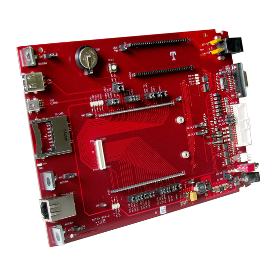
For detailed information about the CoreCDP Development Platform, please visit the Multi-Tech website at: http://www.multitech.net/ An illustration of the developer board follows. MultiConnect® OCG-E MT100EOCG-EV3 Developer Guide... - Page 6 DEVELOPER’S KIT AND DEVELOPER’S BOARD OVERVIEW MultiConnect® OCG-E MT100EOCG-EV3 Developer Guide...
-
Page 7: Product Ordering Options
DEVELOPER’S KIT AND DEVELOPER’S BOARD OVERVIEW The developer’s board is available without a cellular modem. You can also develop your solution by choosing an MT100EOCG model that uses the standard you desire: GPRS, by selecting the MT100EOCG-G2 model HSPA or HSDPA, by selecting the MT100EOCG-H5 model EV-DO Rev A, by selecting the MT100EOCG-EV3 model For complete ordering details, see the section “Product Ordering Options”... -
Page 8: Developer's Board Components
DEVELOPER’S KIT AND DEVELOPER’S BOARD OVERVIEW Universal power supply: 100-240V 9V-1.7A changeable blade power supply Three removable blades (US, EURO and UK) Cables One DB9 serial cable One 3-pin serial cable (debug) One USB host cable One USB device cable One 36-pin GPIO cable One RJ-45 Ethernet cable One RJ-11 phone cable... -
Page 9: Pin Descriptions Of Board To Board Connector
DEVELOPER’S KIT AND DEVELOPER’S BOARD OVERVIEW Pin Descriptions of Board to Board Connector The MultiConnect OCG-E gateway connects to the developer board using an 80-pin board to board connector. This section describes the connector’s pins. Signal Name In/Out Description DC Input Power. 5V DC power. DC Input Power. - Page 10 DEVELOPER’S KIT AND DEVELOPER’S BOARD OVERVIEW Signal Name In/Out Description ADC0 Analog-to-Digital converter Input. (0 to 3v). ADC2 Analog-to-Digital converter Input. (0 to 3v). GPI7 General-Purpose Input. GPI9 General-Purpose Input. JTAG Data Output. NTRST JTAG Reset (Active Low). GPS-PPS GPS PPS - Pulse Per Second. GPS-TX GPS - Transmit Data.
- Page 11 DEVELOPER’S KIT AND DEVELOPER’S BOARD OVERVIEW Signal Name In/Out Description USBH_DN USB Host Data Negative. Negative pin of USB data pair. Logic Ground. USBD_DN USB Device Data Negative. Negative pin of USB data pair. USBD_DP USB Device Data Positive. Positive pin of USB data pair USBD_VBUS USB Device Voltage Sense.
- Page 12 DEVELOPER’S KIT AND DEVELOPER’S BOARD OVERVIEW Signal Name In/Out Description -LED_2 General Purpose LED2 output. (status). -LED_1 General Purpose LED1 output. I2C Data. I2C Clock. -TXD-Debug Transmitted Data. The DTE uses the -TXD3 line to send data to the gateway for transmission of Debug information. -RXD-Debug Received Data.
-
Page 13: Block Diagram
DEVELOPER’S KIT AND DEVELOPER’S BOARD OVERVIEW Block Diagram MultiConnect® OCG-E MT100EOCG-EV3 Developer Guide... -
Page 14: Schematic 1
DEVELOPER’S KIT AND DEVELOPER’S BOARD OVERVIEW Schematic 1 MultiConnect® OCG-E MT100EOCG-EV3 Developer Guide... -
Page 15: Schematic 2
DEVELOPER’S KIT AND DEVELOPER’S BOARD OVERVIEW Schematic 2 MultiConnect® OCG-E MT100EOCG-EV3 Developer Guide... -
Page 16: Schematic 3
DEVELOPER’S KIT AND DEVELOPER’S BOARD OVERVIEW Schematic 3 MultiConnect® OCG-E MT100EOCG-EV3 Developer Guide... -
Page 17: Schematic 4
DEVELOPER’S KIT AND DEVELOPER’S BOARD OVERVIEW Schematic 4 MultiConnect® OCG-E MT100EOCG-EV3 Developer Guide... -
Page 18: Schematic 5
DEVELOPER’S KIT AND DEVELOPER’S BOARD OVERVIEW Schematic 5 MultiConnect® OCG-E MT100EOCG-EV3 Developer Guide... -
Page 19: Schematic 6
DEVELOPER’S KIT AND DEVELOPER’S BOARD OVERVIEW Schematic 6 MultiConnect® OCG-E MT100EOCG-EV3 Developer Guide... -
Page 20: Schematic 7
DEVELOPER’S KIT AND DEVELOPER’S BOARD OVERVIEW Schematic 7 Technical Specifications All models of the MultiConnect OCG-E gateway share the following specifications. Specifications that are unique to a particular model are documented in the chapter dedicated to the model. Category Description Operating Voltage 5VDC +/- 10% Dimensions... -
Page 21: Mt100Eocg-Dk Leds Description
DEVELOPER’S KIT AND DEVELOPER’S BOARD OVERVIEW MT100EOCG-DK LEDs Description LED 1 General Purpose LED1 output. LED 2 General Purpose LED2 output (status). LED 3 General Purpose LED3 output (link status). LED 4 General Purpose LED4 output. LED 5 General Purpose LED5 output. LED 6 General Purpose LED6 output. -
Page 22: Vehicle Safety
Do not place the device alongside computer discs, credit or travel cards, or other magnetic media. The information contained on discs or cards may be affected by the device. Using accessories, such as antennas, that MultiTech has not authorized or that are not compliant with MultiTech's accessory specifications may invalidate the warranty. -
Page 23: Securing Your Device
DEVELOPER’S KIT AND DEVELOPER’S BOARD OVERVIEW build-up, use proper precautions to avoid exposure to electronic discharge during handling and mounting the device. Securing Your Device Respect all local regulations. Become familiar with and use the security features to block unauthorized use and theft. -
Page 24: Chapter 2 - Installing Gateways On The Developer Board
INSTALLING GATEWAYS ON THE DEVELOPER BOARD Chapter 2 – Installing Gateways on the Developer Board Installing Gateways on the Developer Board These topics describe how to install gateways on the developer board. You can install a Multi-Connect OCG-E gateway or, optionally, a universal socket communications device. Installing a MultiConnect OCG-E Gateway onto the Board To install a MultiConnect OCG-E gateway: Align the 80-pin connector on the bottom of the gateway with the 80-pin connector on the developer... -
Page 25: Installing A Universal Socket Communications Device Onto The Board
INSTALLING GATEWAYS ON THE DEVELOPER BOARD If you are installing a MultiConnect OCG-E gateway with a cellular wireless network, connect the cellular antenna lead to the antenna connector on the MultiConnect OCG-E gateway. If you are installing a MultiConnect OCG-E gateway with a GPS receiver, first connect the cellular antenna lead to the cellular antenna connector on the gateway, then connect the GPS antenna lead to the GPS antenna connector on the gateway. -
Page 26: General Purpose Input Output (Gpio) Cable
INSTALLING GATEWAYS ON THE DEVELOPER BOARD General Purpose Input Output (GPIO) Cable GPIO Connector Pin Out Pin Number Name Input/Output Description EXT_IN_0 General-Purpose Input. EXT_IN_1 General-Purpose Input. EXT_IN_2 General-Purpose Input. EXT_IN_3 General-Purpose Input. EXT_IN_4 General-Purpose Input. EXT_IN_5 General-Purpose Input. GPIO11 General-Purpose Input/Output. -
Page 27: Notes
INSTALLING GATEWAYS ON THE DEVELOPER BOARD Pin Number Name Input/Output Description EXT_IN_GND Logic Ground from external. A_GND_OUT Logic Ground from analog side of ADC. ANA_IN_1 Analog-to-Digital converter Input (0 to 3v). ANA_IN_2 Analog-to-Digital converter Input (0 to 3v). ANA_IN_3 Analog-to-Digital converter Input (0 to 3v). ANA_IN_4 Analog-to-Digital converter Input (0 to 3v). - Page 28 INSTALLING GATEWAYS ON THE DEVELOPER BOARD > 2.3 V for a high < 1V for a low GPI pins are 5 V tolerant. GPI pins have a 10K pull-downs to ground. This increases the input current to 330 uA from the standard 1uA. GPO pins output range: >...
-
Page 29: Debug Cable
INSTALLING GATEWAYS ON THE DEVELOPER BOARD Debug Cable MT100EOCG Electrical Characteristics Operating Conditions Units Volts Parameter Minimum Maximum Supply Range - Vcc Absolute Maximum Rating Units Volts Parameter Minimum Maximum Voltage at any signal pin -0.3 Reset -0.3 -0.3 ADC Operating Range Units Volts ADC input operating range DC Electrical Characteristics GPIO1-4/GP15-10/LED1,4,5,6 Units - Volts Parameter... - Page 30 INSTALLING GATEWAYS ON THE DEVELOPER BOARD Parameter Minimum Maximum Digital signal output low level Digital signal output high level DC Electrical Characteristics-LED3 Unit - Volts Output is open drain with 10k pullup DC Electrical Characteristics Reset Unit - Volts Parameter Minimum Maximum Reset (low active) input low...
-
Page 31: Chapter 3 - Troubleshooting
TROUBLESHOOTING Chapter 3 – Troubleshooting Restoring the U-Boot Memory or the Bootstrap Memory If the U-boot memory or the bootstrap memory becomes corrupted, you can restore either of them. Before You Begin You need to short out a resistor to run internal boot code instead of code in bootstrap or u-boot memory. To do this, find some tweezers that fit around the resistor. -
Page 32: Installing Atmel Sam-Ba Utility
TROUBLESHOOTING Installing Atmel SAM-BA Utility This topic describes how to restore memory by using the Atmel SAM-BA utility, connecting with the hardware, mounting the serial driver and restoring the bootstrap memory or u-boot memory. If you have not already done so, download the Atmel SAM-BA utility and unzip the utility package onto your Linux development system: http://www.atmel.com/tools/ATMELSAM-BAIN- SYSTEMPROGRAMMER.aspx Connect the USB cable between Linux system and the MTEOCG hardware. - Page 33 TROUBLESHOOTING kernel: cdc_acm: v0.26:USB Abstract Control Model driver for USB modems and ISDN adapters To connect to your board, use /dev/ttyACMX. Using the Atmel SAM-BA utility to restore memory To run the utility, type: # ./sam-ba Select your board at91sam9g20-ek and click Connect. Select NandFlash.
-
Page 34: Chapter 4 - Design Considerations
DESIGN CONSIDERATIONS Chapter 4 – Design Considerations Noise Suppression Design Adhere to engineering noise-suppression practices when designing a printed circuit board (PCB). Noise suppression is essential to the proper operation and performance of the modem and surrounding equipment. Any OEM board design must consider both on-board and off-board generated noise that can affect digital signal processing. -
Page 35: Electromagnetic Interference
Technical Requirements (grounding/bonding systems, personnel grooming, protected areas, packaging, marking, equipment, and handling), and Sensitivity Testing. MultiTech strives to follow these recommendations. Input protection circuitry is incorporated in MultiTech devices to minimize the effect of static buildup. Take precautions to avoid exposure to electrostatic discharge during handling. - Page 36 DESIGN CONSIDERATIONS MultiTech uses and recommends that others use anti-static boxes that create a faraday cage (packaging designed to exclude electromagnetic fields). MultiTech recommends that you use our packaging when returning a product and when you ship your products to your customers.
-
Page 37: Chapter 5 - Oem Integration
OEM INTEGRATION Chapter 5 – OEM Integration FCC Grant Notes The OEM should follow all the grant notes listed below. Otherwise, further testing and device approvals may be necessary. The antenna gain, including cable loss, for the radio you are incorporating into your product design must not exceed the requirements at 850 MHz and 1900 MHz as specified by the FCC grant for mobile operations and fixed mounted operations as defined in 2.1091 and 1.1307 of the FCC rules for satisfying RF exposure compliance. -
Page 38: Host Labeling
OEM INTEGRATION Mobile: (§2.1091) — A mobile device is defined as a transmitting device designed to be used in other than fixed locations and to generally be used in such a way that a separation distance of at least 20 centimeters is normally maintained between the transmitter’s radiating structure(s) and the body of the user or nearby persons. -
Page 39: Chapter 6 - Cellular Information
CELLULAR INFORMATION Chapter 6 – Cellular Information Antenna System Cellular Devices The cellular/wireless performance depends on the implementation and antenna design. The integration of the antenna system into the product is a critical part of the design process; therefore, it is essential to consider it early so the performance is not compromised. -
Page 40: Sma-To-Ufl And Rsma-To-Ufl Coaxial Cables
CELLULAR INFORMATION Category Description TRP/TIS Including cable loss the total radiate power (TRP) at the antenna can be no less than +22/24.5 dBm for 850/1900 MHz respectively, and the total isotropic sensitivity (TIS) at the antenna can be no less than -99/101.5 dBm for 850/1900 MHz respectively. SMA-to-UFL and RSMA-to-UFL Coaxial Cables Your product includes the following cables: Two SMA-to-UFL cables. -
Page 41: Antennas Available From Multi-Tech
CELLULAR INFORMATION Antennas Available from Multi-Tech Part Number Description Quantity Quad Band ANQB-1HRA Hinged Right Angle 800/900/1800/1900 MHz Cellular Antenna, 7.5" ANQB-10HRA Hinged Right Angle 800/900/1800/1900 MHz Cellular Antenna, 7.5" ANQB-50HRA Hinged Right Angle 800/900/1800/1900 MHz Cellular Antenna, 7.5" Penta Band ANPB-1HRA Hinged Right Angle Penta Band Antenna ANPB-10HRA... -
Page 42: Activating Accounts For Cellular Devices
Some Multi-Tech products have been pre-configured to operate on a specific cellular network. However, before you can begin to use the modem, you must set up a cellular data account with your cellular network provider. Refer to Multi-Tech’s Cellular Activation Web site http://www.multitech.com/activation.go for information on activating your cellular modem. - Page 43 CELLULAR INFORMATION 1 Multi-Tech model identification 2 Multi-Tech ordering part number 3 MEID: mobile equipment identifier in Hexadecimal format Example GPRS Label on End Product MultiConnect® OCG-E MT100EOCG-EV3 Developer Guide...
- Page 44 CELLULAR INFORMATION 1 Host device model identification 2 Multi-Tech OCG-E model identification 3 IMEI: international mobile equipment identity Providing Other Information to the Cellular Carrier A cellular carrier may also ask for the following information: For CDMA OCG-E gateways: The gateway's MEID (Mobile Equipment Identifier) written in hexadecimal format is printed under the barcode on the modem.
-
Page 45: Chapter 7 - Mt100Eocg-Ev3 Model Overview
Related Documentation Use the EV-DO AT Commands to configure the MT100EOCG-EV3 model. These commands are documented in the EV-DO and CDMA AT Commands Reference Guide part number S000546x. You can download this manual from the Multi-Tech website. http://www.multitech.com/en_US/DOCUMENTS/Collateral/Manuals/ MT100EOCG-EV3 Specifications Category... - Page 46 MT100EOCG-EV3 MODEL OVERVIEW Category Description Humidity 20% to 90% non-condensing Power Requirements Operating Voltage Supply range: 4.75 V to 5.25 V 1.1A nominal current Device may be damaged if voltage exceeds 5.5 V Input Power USB bus powered Point-to-Point messaging Mobile-Terminated SMS Mobile-Originated SMS Certifications, Compliance, Warranty...
-
Page 47: Mechanical Drawing Mt100Eocg-Ev3-Gp
MT100EOCG-EV3 MODEL OVERVIEW Mechanical Drawing MT100EOCG-EV3-GP MultiConnect® OCG-E MT100EOCG-EV3 Developer Guide... -
Page 48: Power Measurements
MT100EOCG-EV3 MODEL OVERVIEW Power Measurements Cellular call box Measured current Peak TX (amps) Total inrush charge connection no data (amps) at maximum measured in (amps) power MilliCoulombs (mC) 5 volts US Cellular 800Mhz 0.319 0.817 0.868 2.60 US PCS 1900MHz 0.326 0.843 0.896... - Page 49 MT100EOCG-EV3 MODEL OVERVIEW Category Description Maximum output power (CDMA 1x RTT & EV-DO 1x +24 dBm ± 1 dBm Rev 0/Rev A) MultiConnect® OCG-E MT100EOCG-EV3 Developer Guide...
Need help?
Do you have a question about the MultiConnect MT100EOCG-G2 and is the answer not in the manual?
Questions and answers