Advertisement
Quick Links
®
Introduction
The ISL6560/62 Evaluation Board was designed to
accommodate either the ISL6560 or the ISL6562 power
supply controller ICs. CORE voltage is set by a five bit DAC
that is usually programmed by the microprocessor. For this
board, DAC codes are entered via a five position dip switch.
Power supply input voltages may be applied through three
banana posts or an ATX connector on the board. With an
ATX supply the main input voltage to the converter is 5V. The
ATX 12V supply powers the ISL6560/62, the HIP6601 gate
drivers and the transient load generator. A toggle switch is
provided on the board to enable the ATX supply.
Converter input voltage via the banana connectors can
range from 5V to 12V. A separate connector supplies 12V to
the ISL6560/62, transient load generator and the gate
drivers as described above.
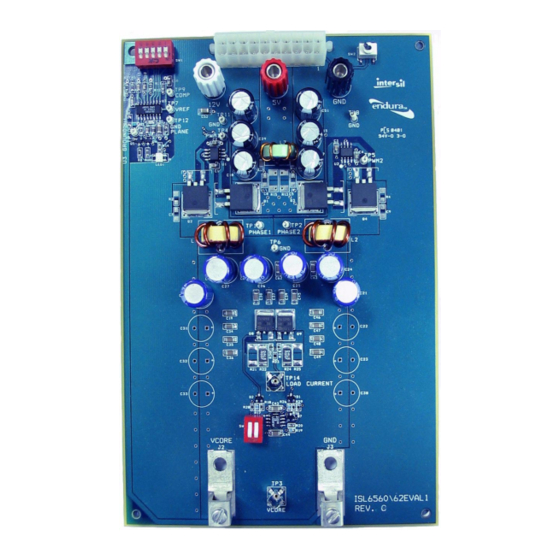
Figure 1 shows the Evaluation Board. Note the ATX
connector at the top of the board. The ATX power switch
SW2, is located to the right of the connector.
FIGURE 1. EVALUATION BOARD
Application Note
1
1-888-INTERSIL or 321-724-7143
ISL6560/62 Evaluation Board
April 2002
Description
This board was design so that a wide range of input voltages
could be used. Burndy binding posts at the lower end of the
board provide the high current connections for the output
load.
Just above the output connectors is a pulse generator to
provide 40A transient loading to verify response to pulse
loading of the supply. Scope probe connectors monitor the
current pulse, and output voltage.
Extra output capacitor locations are available to modify the
output capacitor configuration or type of capacitors. 22µF
ceramic capacitors accompany the bulk electrolytic
capacitors. In an application where the supply is connected
to an active load, high frequency capacitors should be
located as close as possible to the load to help reduce
undesired transient voltage changes at the load.
The ISL6560/62 is located on the left side of the board.
Immediately below the controller IC is the POWER GOOD
monitoring circuit. A dual RED-GREEN LED indicator is
green when the CORE voltage is within the defined data
sheet limits. Figure 13 shows a schematic diagram of the
POWER GOOD monitoring circuit.
ISL6560 and ISL6562
Figure 2 shows a simplified functional block diagram of these
devices, outlining the major differences between the two ICs.
WRGD
VID4
VID3
VID2
D/A
VID1
VID0
FB
COMP
DAC Codes
ISL6560 - VRM 9.0
ISL6562 - VRM 8.5
FIGURE 2. SIMPLIFIED BLOCK DIAGRAM SHOWING
MAJOR DEVICE DIFFERENCES
CAUTION: These devices are sensitive to electrostatic discharge; follow proper IC Handling Procedures.
|
Intersil (and design) is a registered trademark of Intersil Americas Inc.
Author: Hal Wittlinger
VCC
REF
UVLO and
3V REF
BIAS CIRCUITS
OSCILLATOR
+
UV
X0.82
-
CONTROL
+
_
LOGIC
OVP
-
X1.24
CMP
+
E/A
-
GND
CS Threshold Voltage
ISL6560 - 157mV
ISL6562 - 79mV
Copyright © Intersil Americas Inc. 2002. All Rights Reserved
AN1009.0
CT
PWM1
PWM2
CS+
+
-
CS-
Advertisement

Related Manuals for Intersil ISL6560


Summary of Contents for Intersil ISL6560
- Page 1 Figure 1 shows the Evaluation Board. Note the ATX The ISL6560/62 is located on the left side of the board. connector at the top of the board. The ATX power switch Immediately below the controller IC is the POWER GOOD SW2, is located to the right of the connector.
- Page 2 ISL6560/62 Evaluation Board The ISL6560 has a DAC scaled for VRM9.0 codes while the or a switch. This device should be located next the COMP ISL6562’s DAC is set to VRM8.5 codes. The other major pin to reduce the possibility of external pickup by the pin.
-
Page 3: Pc Board Layout Considerations
ISL6560/62 Evaluation Board Efficiency Transient Load Generator Figures 8 and 9 show the efficiency of the converter with Probably one of the most interesting tests for a regulator CORE voltage at the two extremes of the DAC voltage and at system is the transient load. - Page 4 System Schematic Diagram of Figure 10. The ground con- due to component placement and space constraints. The nection, pin 9 of the ISL6560 should be connected to the following text reviews these layout considerations in more system ground at the load.
- Page 5 BOOT PVCC C34-37, 900nH C45-49, Q4 HUF76145 C60-63 LGATE HIP6601ECB 1µF FIGURE 11. SCHEMATIC DIAGRAM OF A 40A SUPPLY USING THE ISL6560 CONTROLLER AND HIP6601 GATE DRIVERS To CORE Plan 732Ω Q9 HUF78129 4.7µF 324Ω BAV99TA Current Monitoring HIP2100 HUF78129 732Ω...
- Page 6 ISL6560/62 Evaluation Board To PWRGD Pin 10 GREEN LED 1 LED 1A 120k 3.3k 3.3k 2N7002 2N7002 FIGURE 13. SCHEMATIC DIAGRAM OF THE POWER GOOD MONITORING CIRCUIT CAll 1-888 Intersil FIGURE 14. SILK SCREEN...
- Page 7 ISL6560/62 Evaluation Board FIGURE 15B. GROUND PLAN FIGURE 15A. TOP COPPER FIGURE 15C. POWER PLAN FIGURE 15D. BOTTOM COPPER FIGURES 15A-D. Showing ALL FOUR LAYERS OF THE PC BOARD...
- Page 8 ISL6560/62 Evaluation Board TABLE 1. Bill of Materials Quantity Reference Part PCB Footprint Vendor Part Number C1,C3 0.1uF, 25V, X7R P0805 Various Ceramic C2,C4 1uF, 25V, X7R P0805 Various Ceramic C5,C8, Not Populated P1206 C7,C9 Not populated P1206 C10, C12...
-
Page 9: Test Points
ISL6560/62 Evaluation Board TABLE 1. Bill of Materials (contiued) 330Ω, 5% P0805 Various R10,R8 3.3K, 5% P0805 Various 120K, 5% P0805 Various 22K, 5% P0805 Various 15K, 5% P0805 Various 5mΩ, 1% P2512 Panasonic ERJM1WSF5M0U, 0.005 1% 5mΩ, 1% f o r P2512 Not populated. - Page 10 ISL6560 Supply Design Sequence The ISL6560 data sheet describes in more detail the following equations. There are several changes from the computations in the body of the data sheet. First, an operating frequency of 400kHz was chosen. Next, this design sequence shows the method of setting the initial no load voltage at the DAC setting and offsetting the no load voltage 15mV above the programmed DAC voltage.
- Page 11 Accordingly, the reader is cautioned to verify that data sheets are current before placing orders. Information furnished by Intersil is believed to be accurate and reliable. However, no responsibility is assumed by Intersil or its subsidiaries for its use; nor for any infringements of patents or other rights of third parties which may result from its use.
- Page 12 Mouser Electronics Authorized Distributor Click to View Pricing, Inventory, Delivery & Lifecycle Information: Intersil ISL6560EVAL1 ISL6562EVAL1...
Need help?
Do you have a question about the ISL6560 and is the answer not in the manual?
Questions and answers