Advertisement
Quick Links
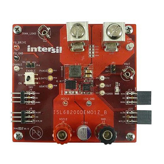
ISL68200DEMO1Z
Demonstration Board User Guide
The
ISL68200
is a single-phase synchronous buck PWM
controller featuring Intersil's proprietary R4™ Technology,
which has extremely fast transient performance, accurately
regulated frequency control, and all internal compensation.
The ISL68200 supports a wide 4.5V to 24V input voltage range
and a wide 0.5V to 5.5V output range. It includes
programmable functions and telemetries for easy use and
high system flexibility using SMBus, PMBus, or I
See the ISL68200 datasheet for more details.
The ISL68200DEMO1Z is a 6-layer board demonstrating a
compact 17mmx17mm 20A synchronous buck converter.
Transient performance, fault protections, DC/AC regulations,
PMBus programming, power sequencing, margining, and other
features can be evaluated using this board.
The PMBus dongle (ZLUSBEVAL3Z USB-to-PMBus adapter) and
USB cable are included with the demonstration board.
Intersil's evaluation software can be installed from Intersil's
website and be used to evaluate the full PMBus functionality of
the part using a PC running Microsoft Windows.
Related Literature
• For a full list of related documents, visit our website
-
ISL68200
product page
• Intersil's
PowerNavigator
User Guide
2
I
C/SMBus/
PGOOD
UG067 Rev.2.00
Aug 23, 2017
2
C interface.
1.0µ F
VCC
7VLDO
1.0µ F
SALERT
SCL
PMBus
SDA
PGOOD
EN
EN
IOUT
VCC
4
PROG1-4
SGND
FIGURE 1. ISL68200DEMO1Z SIMPLIFIED SCHEMATIC
Key Features
• 20A synchronous buck converter with PMBus control
• On-board transient load with adjustable di/dt
• Configurable through resistor pins
• Cascadeable PMBus connectors
• Integrated LDOs for a single rail solution
• Enable switch and power-good indicator
• All ceramics solution with SP capacitor footprint option
Target Specifications
• V
= 4.75V to 14.5V
IN
• V
= 1V/20A full load
OUT
• f
= 400kHz
SW
• Peak efficiency:
- 89% at 12A/1V
- 94% at 6A/1.8V
• Output regulation: 1V ±8mV
• I/O capacitor rating: C
• Compact size: 17mmx17mm
• With or without PMBus, SMBus, and I
Ordering Information
PART NUMBER
ISL68200DEMO1Z ISL68200 Demonstration Board (Items shipped:
Demonstration board, dongle, USB cable)
4.7µ F
PVCC
VIN
0.1µF
BOOT
UGATE
PHASE
LGATE
VCC
10k
NTC
1.54k
NTC
0.1µF
CSEN
CSRTN
VSEN
RGND
PGND
USER'S MANUAL
Aug 23, 2017
/12V
OUT
IN
/5V
OUT
IN
- 16V; C
- 4V
IN
OUT
2
C Capability
DESCRIPTION
4.75 TO 15V
1V AT 20A
Page 1 of 22
UG067
Rev.2.00
Advertisement

Related Manuals for Intersil ISL68200 Series


Summary of Contents for Intersil ISL68200 Series
- Page 1 USB cable are included with the demonstration board. • f = 400kHz Intersil’s evaluation software can be installed from Intersil’s website and be used to evaluate the full PMBus functionality of • Peak efficiency: the part using a PC running Microsoft Windows.
- Page 2 Intersil’s PowerNavigator evaluation software is compatible with with Intersil’s R4 Modulator, 8-bit programmable boot voltage Windows operating systems and can be used to evaluate the levels, selectable switching frequency in continuous conduction serial bus functionality of the ISL68200. The software and user...
-
Page 3: Load Transient
ISL68200DEMO1Z Configuration Load Transient The default programming pins setting of the ISL68200DEMO1Z The on-board transient load can be controlled by a function board can be found at the resistor reader table on the upper right generator, whose inputs are connected to FG_DRIVE2 and corner of “ISL68200DEMO1Z Schematics”... -
Page 4: Design Modifications
ISL68200DEMO1Z Design Modifications fine-tuning might be needed depending upon the rework and final layout design. Any modifications to the design will require new L/DCR matching For the 5V input voltage applications with 4.5V < V < 5.5V for a different inductor, a divider on the PROG pins for a different requirement, the VIN, VCC, PVCC, and 7VLDO pins should be operational configuration, RSEN1 for OCP, and an IOUT network shorted together, to connect with the input supply for optimal... - Page 5 ISL68200DEMO1Z Design and Layout TABLE 2. DESIGN AND LAYOUT CHECKLIST (Continued) Considerations NOISE NAME SENSITIVITY DESCRIPTION To ensure a first pass design, the schematics design must be SCL, SDA 50kHz to 1.25MHz signal when the SMBus, done correctly and the board must be carefully laid out. PMBus, or I C is sending commands.
- Page 6 ISL68200DEMO1Z TABLE 2. DESIGN AND LAYOUT CHECKLIST (Continued) TABLE 3. TOP LAYOUT TIPS NOISE NUMBER DESCRIPTION NAME SENSITIVITY DESCRIPTION The layer next to controller (top or bottom) should be a ground PROG1-4 Resistor divider must be referenced to the VCC layer.
- Page 7 ISL68200DEMO1Z Schematics RESISTOR READER BOOT VOTLAGE = 1V PROG1 PFM DISABLED, TCOMP=15degC, ADDR = C0/C1h PROG2 PROG3 25k Clamp Disabled, OCP/OTP Retry, 400kHz, AV=42 PROG4 SS = 1.25mV/us; RR = 200k Ohm;AVMULTI=1X NCP15XH103J03RC 0402 size FIGURE 6. ISL68200DEMO1Z 1V AT 20A BUCK SOLUTION SCHEMATICS...
- Page 8 ISL68200DEMO1Z Schematics (Continued) R12 = 9.09K for typical POR = 10.08V/9.12V; R12 = 24.9K for typical POR = 4.21V/3.81V VOUT PGOOD LED LIGHT DOWN VOUT STATUS Place Connection of VOUT and GND to the Remote Sensing Points (Say center DNP these and leave the holes for probes of the Ceramic Caps or Last Ceramic Cap) ON LEFT OF BOARD (MALE)
-
Page 9: Bill Of Materials
ISL68200DEMO1Z Bill of Materials REFERENCE DESIGNATOR DESCRIPTION PCB FOOTPRINT MANUFACTURER PART NUMBER R4 Wrapper with Driver QFN24_157X157_197_EPC INTERSIL ISL68200IRZ-REVD CIN1 270µF/16V/8x9/10mΩ CAPR_315X275_150_P SANYO 16SEPC270MX 4.7µF/6.3V/X5R SM0603 VENKEL C0603X5R6R3-475KNE C2, C3 1.0µF/16V/X7R SM0603 C1608X7R1C105K 1µF/6.3V/X5R SM0603 PANASONIC ECJ1VB0J105K 22nF/50V/X7R SM0603 VENKEL C0603X7R500-223KNE C6, CB1, CC1, CNTC1 0.1µF/16V/X7R... - Page 10 ISL68200DEMO1Z Bill of Materials (Continued) REFERENCE DESIGNATOR DESCRIPTION PCB FOOTPRINT MANUFACTURER PART NUMBER Female Banana Jack, Red 111-07xx-001 JOHNSON 111-0702-001 COMPONENTS J8, J9 CONN-HEADER, 2X3, BRKAWY, CONN6 SAMTEC TSW-103-08-T-D-RA 2.54mm,TIN J10, J11 CONN-SOCKET STRIP,TH,2X3, CONN6 SAMTEC SSQ-103-02-T-D-RA 2.54mm,TIN JP1, JP4 2-pin 0.1'' spacing Jumper CONN2 BERG/FCI...
-
Page 11: Measured Data
ISL68200DEMO1Z Measured Data The following data was acquired using a ISL68200DEMO1Z board. 0.25 0.20 0.15 0.10 0.05 0.00 SLOPE = 1 -0.05 LOAD CURRENT (A) FIGURE 8. TYPICAL DIGITAL OUTPUT CURRENT MEASUREMENT VOUT=0.8V VOUT=0.8V VOUT=1V VOUT=1V VOUT=1.2V VOUT=1.2V VOUT=1.5V VOUT=1.5V VOUT=1.8V VOUT=1.8V LOAD CURRENT (A) - Page 12 ISL68200DEMO1Z Measured Data The following data was acquired using a ISL68200DEMO1Z board. (Continued) VOUT=0.8V VOUT=1V VOUT=0.8V VOUT=1V VOUT=1.2V VOUT=1.5V VOUT=1.2V VOUT=1.5V VOUT=1.8V VOUT=1.8V LOAD CURRENT (A) LOAD CURRENT (A) FIGURE 13. EFFICIENCY, V = 12V, f = 600kHz FIGURE 14. EFFICIENCY, V = 5V, f = 600kHz 87.5...
- Page 13 ISL68200DEMO1Z Measured Data The following data was acquired using a ISL68200DEMO1Z board. (Continued) 100mV/DIV 100mV/DIV 10V/DIV 10V/DIV 100µs/DIV 100µs/DIV FIGURE 20. V RAMP-DOWN FROM 1V TO 0.5V IN PWM MODE FIGURE 19. V RAMP-UP FROM 0.5V TO 1V IN PWM MODE (CH1-V , CH2-PHASE) (CH1-V...
- Page 14 ISL68200DEMO1Z Measured Data The following data was acquired using a ISL68200DEMO1Z board. (Continued) 20mV/DIV 20mV/DIV 10A/DIV 10A/DIV 10V/DIV 10V/DIV 5µs/DIV 5µs/DIV FIGURE 26. STEP RESPONSE TO LOAD RELEASE AT PWM MODE, FIGURE 25. STEP RESPONSE TO LOAD STEP AT PWM MODE, = 1V, f = 400kHz, LOAD PROFILE: 0.25A TO = 1V, f...
- Page 15 ISL68200DEMO1Z ISL68200DEMO1Z Board Layout FIGURE 31. PCB - TOP ASSEMBLY UG067 Rev.2.00 Page 15 of 22 Aug 23, 2017...
- Page 16 ISL68200DEMO1Z ISL68200DEMO1Z Board Layout (Continued) FIGURE 32. PCB - TOP LAYER UG067 Rev.2.00 Page 16 of 22 Aug 23, 2017...
- Page 17 ISL68200DEMO1Z ISL68200DEMO1Z Board Layout (Continued) FIGURE 33. PCB - INNER LAYER 2 (TOP VIEW) UG067 Rev.2.00 Page 17 of 22 Aug 23, 2017...
- Page 18 ISL68200DEMO1Z ISL68200DEMO1Z Board Layout (Continued) FIGURE 34. PCB - INNER LAYER 3 (TOP VIEW) UG067 Rev.2.00 Page 18 of 22 Aug 23, 2017...
- Page 19 ISL68200DEMO1Z ISL68200DEMO1Z Board Layout (Continued) FIGURE 35. PCB - INNER LAYER 4 (TOP VIEW) UG067 Rev.2.00 Page 19 of 22 Aug 23, 2017...
- Page 20 ISL68200DEMO1Z ISL68200DEMO1Z Board Layout (Continued) FIGURE 36. PCB - INNER LAYER 5 (TOP VIEW) UG067 Rev.2.00 Page 20 of 22 Aug 23, 2017...
- Page 21 ISL68200DEMO1Z ISL68200DEMO1Z Board Layout (Continued) FIGURE 37. PCB - BOTTOM LAYER (TOP VIEW) UG067 Rev.2.00 Page 21 of 22 Aug 23, 2017...
- Page 22 All trademarks and registered trademarks are the property of their respective owners. Intersil Corporation reserves the right to make changes in circuit design, software and/or specifications at any time without notice. Accordingly, the reader is cautioned to verify that the document is current before proceeding.
Need help?
Do you have a question about the ISL68200 Series and is the answer not in the manual?
Questions and answers