Table of Contents
Advertisement
RFID System
V680 Series
User's Manual
ID Sensor Units
CS1W-V680C11
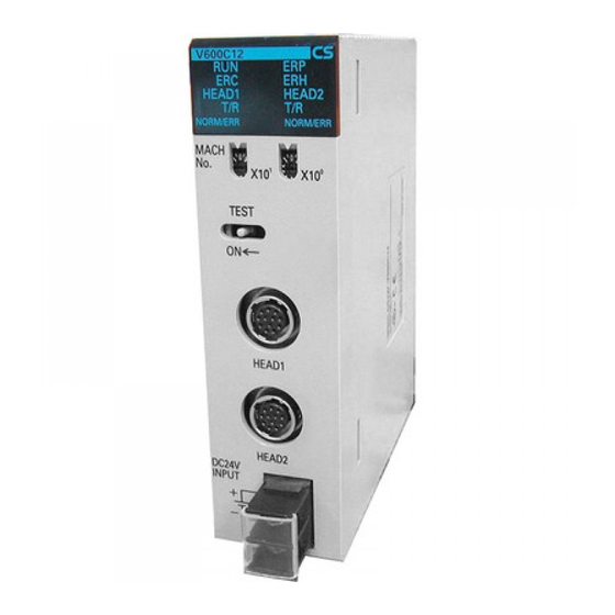
CS1W-V680C12
CJ1W-V680C11
CJ1W-V680C12
P
E R
H
1
E R
C 1
2
A D
8 0
H E
V 6
N
R U
T / R
C
R
/E R
E R
1
R M
A D
N O
H E
T / R
R
/E R
R M
N O
S T
T E
O N
A D
H E
P
E R
H
2
E R
C 1
2
A D
8 0
H E
V 6
N
R U
T / R
C
R
/E R
E R
1
R M
A D
N O
H E
T / R
R
/E R
R M
N O
S T
T E
O N
1
A D
H E
2
A D
H E
V
2 4
D C
T
P U
I N
+
-
Man. No.: Z271-E1-07
Advertisement
Chapters
Table of Contents
Troubleshooting

Related Manuals for Omron CS1W-V680C11


Summary of Contents for Omron CS1W-V680C11
- Page 1 RFID System V680 Series User’s Manual ID Sensor Units CS1W-V680C11 CS1W-V680C12 CJ1W-V680C11 CJ1W-V680C12 T / R T / R /E R /E R T / R T / R /E R /E R Man. No.: Z271-E1-07...
- Page 2 Introduction Thank you for purchasing an ID Sensor Unit for a V680/V680S-series RFID System. This manual describes the functions, performance, and application methods needed for optimum use of your V680/V680S-series RFID System. Please observe the following items when using the V680/V680S-series RFID System. •...
- Page 3 ID Sensor Unit Functions Section 5 Controlling the ID Sensor Unit Section 6 Troubleshooting Alarms and Errors Section 7 Appendices Section 8 RFID System CS1W-V680C11 ID Sensor Unit CS1W-V680C12 ID Sensor Unit CJ1W-V680C11 ID Sensor Unit CJ1W-V680C12 ID Sensor Unit User's Manual...
- Page 4 Please read and understand this document before using the products. Please consult your OMRON representative if you have any questions or comments. WARRANTY OMRON’s exclusive warranty is that the products are free from defects in materials and workmanship for a period of one year (or other period if specified) from date of sale by OMRON.
- Page 5 Introduction Safety Precautions Signal Words Used in This Manual The following signal words and symbols are used in this manual to indicate precautions that must be observed to ensure safe use of the V680-series ID Sensor Unit. The precautions provided here contain important safety information.
- Page 6 Introduction Warnings WARNING Never attempt to disassemble any Units while power is being supplied. Doing so may result in serious electrical shock or electrocution. Never touch any of the terminals while power is being supplied. Doing so may result in serious electrical shock or electrocution.
- Page 7 Series User's Manual (Cat. No. Z221) and check to make sure there is no mutual interference. 12. If an error is detected in the Product, immediately stop operation and turn OFF the power supply. Consult with an OMRON representative. 13. Dispose of the Product as industrial waste.
- Page 8 Introduction Precautions for Correct Use Always observe the following precautions to prevent operation failure, malfunctions, and adverse effects on performance and equipment. 1. Installation Environment Do not use the Product in the following locations. • Locations exposed to any flammable, explosive, or corrosive gasses •...
- Page 9 Introduction Precautions for Users of V600-series ID Sensor Units Differences between the V600-series and V680-series ID Sensor Units The following features were added to the V680-series ID Sensor Units in comparison to the V600- series Units. Functions are upwardly compatible, so V600-series Units can be easily replaced with V680-series Units.
- Page 10 Introduction Meanings of Symbols Indicates particularly important points related to a function, including precautions and application advice. Indicates page numbers containing relevant information. Indicates reference to helpful information and explanations for difficult terminology. RFID System User's Manual...
-
Page 11: Rfid System
Introduction Table of Contents Introduction Safety Precautions Precautions for Safe Use Precautions for Correct Use Precautions for Users of V600-series ID Sensor Units Meanings of Symbols Table of Contents Features and System Configuration Outline of Features and Functions Using Heat-resistive RF Tags (V680-D1KP58HTN and V680-D1KP58HT) @@ RF Tags Using V680S-D8KF System Configuration... -
Page 12: Table Of Contents
Introduction ID Sensor Unit Functions Operating Modes Communications Specifications Parameter Settings in DM Area RF Tag Memory Write Protection RF Tag Service Life Check RF Tag Memory Check RF Tag Memory Error Correction Controlling the ID Sensor Unit ID Sensor Unit Operation Communications Commands Communications Time Troubleshooting Alarms and Errors... -
Page 13: Rfid System
SECTION 1 Features and System Configuration Outline of Features and Functions Using Heat-resistive RF Tags (V680-D1KP58HTN and V680-D1KP58HT) Using V680S-D8KF @@ RF Tags System Configuration Functions by Application RFID System User's Manual... -
Page 14: Outline Of Features And Functions
DC24V INPUT These ID Sensor Units are used in SYSMAC CS-series PLCs to read and write data for V680-series RF Tags. There are two models: a One-channel ID Sensor Unit (CS1W-V680C11) and a Two-channels ID Sensor Unit (CS1W-V680C12). RFID System... - Page 15 These ID Sensor Units are used in SYSMAC CJ-series PLCs to read and write data for V680-series RF Tags. There are two models: a One-channel ID Sensor Unit (CJ1W-V680C11) and a Two-channels ID Sensor Unit (CJ1W-V680C12). CS1W-V680C11 CS1W-V680C12 CJ1W-V680C11 CJ1W-V680C12...
- Page 16 A different memory map may be used when reading or writing Heat-resistant RF Tags that were written by the V680- CA1D/-CA2D from a Reader/Writer that is manufactured by a company other than OMRON. Refer to Operation When RF Tag Memory Setting Is Set to Standard Mode in this section.
-
Page 17: Using Heat-Resistive Rf Tags (V680-D1Kp58Htn And V680-D1Kp58Ht)
SECTION 1 Features and System Configuration Using Heat-resistive RF Tags (V680-D1KP58HTN and V680-D1KP58HT) This section provides information for using Heat-resistive RF Tags (V680-D1KP58HTN or V680-D1KP58HT). If you are not using a Heat-resistive RF Tag, set the RF Tag memory setting to Standard Mode. Precautions for Saving Data at High Temperatures If you are using Heat-resistive RF Tags (V680-D1KP58HTN or V680-D1KP58HT), write the data again after saving data at a high temperature even if it is not necessary to change the data. - Page 18 SECTION 1 Features and System Configuration Precautions when Setting the RF Tag Memory Setting to CA1D Mode Applicable RF Tags Only the V680-D1KP@@ RF Tags can be used when the RF Tag memory setting is set to CA1D Mode. V680-D@KF@@ RF Tags cannot be used.
- Page 19 SECTION 1 Features and System Configuration Combining ID Sensor Units and ID Controllers The address maps in the RF Tags for the V680-D1KP@@ (except for the V680-D1KP58HT) are reversed between the V680-CA1D/-CA2D ID Controller and CS/CJ1W-V680C1@ ID Sensor Units (with RF Tag memory setting set to CA1D Mode for version 1.2 or newer), and the V680-CA5D01-V2 (ver- sion 2.1 or older) ID Controller and CS/CJ1W-V680C1@ ID Sensor Units (with RF Tag memory setting set to Standard Mode for version 1.2 or newer).
- Page 20 SECTION 1 Features and System Configuration Operation When RF Tag Memory Setting Is Set to Standard Mode When data that was written to a V680-D1KP58HTN RF Tag with the V680-CA1D/-CA2D ID Controller is read from a CS/CJ1W-V680C1@ ID Sensor Unit, the data is read from addresses that are reversed in one-block (eight-byte) units.
- Page 21 SECTION 1 Features and System Configuration Operation When RF Tag Memory Setting Is Set to CA1D Mode If the RF Tag memory setting for the CS/CJ1W-V680C1@ (version 1.2 or newer) is set to CA1D Mode, data is read from or written to addresses that are reversed in block units for the V680-D1KP@@ (except for the V680-D1KP58HT) in the same way as for the V680-CA1D/-CA2D.
- Page 22 SECTION 1 Features and System Configuration @@ RF Tags Using V680S-D8KF To use the V680S-D8KF@@, it must be version 1.2 or newer. (Production since October 2014) The product label describes the “Lot No.” Refer to “Lot No.” and check to the date of manufacture. •...
-
Page 23: System Configuration
Moves (moving body) (moving body) Note: The above example uses one One-channel ID Sensor Unit (CS1W-V680C11) and one Two- channels ID Sensor Unit (CS1W-V680C12). The V680-H01 Antenna can be connected to only the One-channel ID Sensor Unit (CS1W-V680C11). It cannot be connected to the Two-channels ID Sensor Unit (CS1W-V680C12). - Page 24 SECTION 1 Features and System Configuration CJ-series PLCs One-channel ID Sensor Unit CPU Unit Two-channel ID Sensor Unit Amplifier Antenna RF Tag Workpiece Workpiece Moves (moving body) (moving body) Note: The above example uses one One-channel ID Sensor Unit (CJ1W-V680C11) and one Two- channels ID Sensor Unit (CJ1W-V680C12).
- Page 25 C200HW-PA204R C200HW-PD204 C200HW-PA209R The V680-H01 Antenna can be connected to only the One-channel ID Sensor Unit (CS1W-V680C11). It cannot be connected to the Two-channels ID Sensor Unit (CS1W-V680C12). CJ-series PLCs CJ-series ID Sensor Units are classified as CJ-series Special I/O Units.
- Page 26 SECTION 1 Features and System Configuration Mounting Units CS-series PLCs Use the following procedure to mount an ID Sensor Unit to the Backplane. Lock the top of the ID Sensor Unit into the slot on the Backplane. Hook Backplane Rotate the Unit downwards as shown in the following diagram.
- Page 27 SECTION 1 Features and System Configuration CJ-series PLCs ID Sensor Units are connected as I/O Units in the system configuration, as shown below. Power Supply Unit CPU Unit ID Sensor Units End Cover (included with CPU Unit) Use the following procedure to connect an ID Sensor Unit. Align the connectors and press in firmly on the Units to connect them completely.
- Page 28 SECTION 1 Features and System Configuration Unit Handling Precautions • Be sure to turn OFF the power supply to the PLC before installing or disconnecting Units, or connecting lines. • To reduce the influence of electrical noise, wire input and output lines in separate ducts from high- voltage and power lines.
-
Page 29: Functions By Application
SECTION 1 Features and System Configuration Functions by Application Application Function Reference Performing communications tests with RF Tags without programming Test Mode p. 78 the CPU Unit Adjusting communications timing with RF Tags Communications Specifications Examples: p. 85 • Communicating with RF Tags stopped in front of the Antenna •... - Page 30 SECTION 1 Features and System Configuration MEMO RFID System User's Manual...
- Page 31 SECTION 2 CS-series ID Sensor Units Specifications Operating Procedure Part Names and Functions Connections and Wiring RFID System User's Manual...
- Page 32 Note 1. “Rack” indicates either the CPU Rack or an Expansion Rack. 2. The V680-H01 Antenna can be connected only to the CS1W-V680C11 ID Sensor Unit. It cannot be used with the CS1W-V680C12 ID Sensor Unit. 3. If using Intelligent I/O Instructions is specified as the data transfer method, up to 2,048 bytes can be transferred in one scan.
- Page 33 (1) RF Tag Communications Speed (Normal Mode or High-speed Mode) (2) Write Verification (3) Auto Wait Time Setting Communications controls (4) UID Addition Setting (5) Write Protection Disable Setting (6) Antenna Connection Setting (One-channel ID Sensor Unit (CS1W-V680C11)) (7) Results Monitor Output Setting Read Read Write Write...
- Page 34 Input Words to 3, and the Output Words to 7, and select the Repeat IN/OUT for each Address per Unit option. • When using CX-Programmer V2.0 or later with the CS1W-V680C11, “I” will be displayed in the ladder diagram before address for inputs and “Q”...
- Page 35 Operating Procedure Example The following is an operating procedure example for the following conditions. Reading 10 Bytes of Data from RF Tag Address 0010 (Hex) Using a Trigger CS-series CPU Unit CS1W-V680C11 V680C11 Special I/O Unit in CIO Read command...
- Page 36 SECTION 2 CS-series ID Sensor Units ID Sensor Unit Settings Test switch (Set on Unit’s front panel.) TEST T /R /E R T /R /E R Test switch IN P Mounting and Installation Unit Number Setting Set the unit number to 1, and the following words will be allocated to the Unit as a Special I/O Unit.
- Page 37 SECTION 2 CS-series ID Sensor Units Creating I/O Tables Always create the I/O tables after turning ON the PLC power supply. The I/O tables can be created from a CS/CJ-series Programming Console or a CX-Programmer (Support Software used to control a PLC, e.g., to create programs or change operating modes). Peripheral port Programming Console ...
- Page 38 SECTION 2 CS-series ID Sensor Units First word allocated to Unit in DM Area: m = D20000 + (100 × 0) = D20000 Meaning Contents address 15 14 13 12 11 10 UID Addition Test Mode Disable Write Verification Communications D20000 Speed 0: Disabled...
- Page 39 SECTION 2 CS-series ID Sensor Units Ladder Programming Peripheral port Programming Console Set the Command, Communications Specification, Read Data Storage Order, First RF Tag Read Address, Number of Bytes to Read, and Read Data Storage Destination in CIO n+1 to CIO n+6 allocated in the Special I/O Unit Area (here, CIO 2011 to CIO 2016).
- Page 40 SECTION 2 CS-series ID Sensor Units Part Names and Functions Part Names CS1W-V680C11 CS1W-V680C12 (front) (front) V680C11 V680C12 Status indicators HEAD1 HEAD2 NORM/ERR NORM/ERR NORM/ERR Unit number switches TEST TEST Test switch Connector for Amplifier/Antenna 1 HEAD HEAD1 Connector for Amplifier/Antenna 2...
- Page 41 Unit in the Special I/O Unit Area and in Special I/O Unit words the DM Area. The words allocated to the ID Sensor Unit in these two areas are determined by the setting of the unit number switches on the Unit’s front panel. CS1W-V680C11 CS1W-V680C12 Words allocated in...
- Page 42 SECTION 2 CS-series ID Sensor Units Test Switch The test switch on the Unit’s front panel is used to switch between RUN Mode and Test Mode. Specify using the test switch in the Run/Test Switching Method Setting in the DM Area to enable using this switch.
- Page 43 SECTION 2 CS-series ID Sensor Units Connections and Wiring Connecting the Amplifier or Antenna Connection Method Holding the base of the connector, align the white mark on the Unit with the white mark on the connector and insert the connector. Base of connector Press in on the connector until it locks in place.
- Page 44 AWG26 to 18 Forked J.S.T Mfg. Co., Ltd. 1.25-Y3A 6.5 mm max. (For M3 terminal) Recommended DC Power Supplies (Compact, DIN Track-mountable, manufactured by OMRON) Model number Output capacity Input voltage S8VS-03024 24 VDC, 1.3 A 100 to 240 VAC •...
- Page 45 SECTION 2 CS-series ID Sensor Units Wiring for Safety and Noise Immunity Antenna Cable and I/O Signal Lines Wire the Antenna cable and I/O signal lines in separate ducts from power circuit cables both inside and outside the control panel. (1): I/O cables (2): Power lines Floor ducts...
- Page 46 SECTION 2 CS-series ID Sensor Units • Noise Countermeasures for External Wiring Consider the following items when wiring external lines, such as Antenna cable, I/O lines, power supply lines, and high-power lines. • When using multiconductor cables for signal lines, do not use the same cable for both I/O lines and other control lines.
- Page 47 SECTION 3 CJ-series ID Sensor Units Specifications Operating Procedure Part Names and Functions Connections and Wiring RFID System User's Manual...
- Page 48 SECTION 3 CJ-series ID Sensor Units Specifications General Specifications General specifications conform to those of SYSMAC CJ-series Special I/O Units. Performance Specifications CJ1W-V680C11 CJ1W-V680C12 Unit classification Special I/O Unit Influence on CPU Unit's cycle 0.15 ms 0.3 ms time V680-HA63@ Amplifier connected: 5 VDC, 260 mA 5 VDC, 320 mA max.
- Page 49 SECTION 3 CJ-series ID Sensor Units Communications Function Specifications CJ1W-V680C11 CJ1W-V680C12 (1) RF Tag Communications Speed (Normal Mode or High-speed Mode) (2) Write Verification (3) Auto Wait Time Setting Communications (4) UID Addition Setting control (5) Write Protection Disable Setting (6) Antenna Connection Setting (One-channel ID Sensor Unit (CJ1W-V680C11)) (7) Results Monitor Output Setting Read...
- Page 50 SECTION 3 CJ-series ID Sensor Units Operating Procedure The operating procedure for an ID Sensor Unit is shown in the following flowchart. Set switch on front of Unit • Turn OFF the test switch on the front of the Unit. Wire Set unit number •...
- Page 51 SECTION 3 CJ-series ID Sensor Units Operating Procedure Example The following is an operating procedure example for the following conditions. Reading 10 Bytes of Data from RF Tag Address 0010 Using a Trigger. CJ-series CPU Unit CJ1W-V680C11 Special I/O Unit Area RF Tag Read command Address (hex)
- Page 52 SECTION 3 CJ-series ID Sensor Units ID Sensor Unit Settings Test Switch (Set on Unit's front panel.) TEST Test switch Mounting and Installation Unit Number Setting Set the unit number to 1, and the following words will be allocated to the Unit as a Special I/O Unit.
- Page 53 SECTION 3 CJ-series ID Sensor Units Creating I/O Tables Always create the I/O tables after turning ON the PLC power supply. The I/O tables can be created from the Programming Console or CX-Programmer. Peripheral port Programming Console Initial Settings Make the settings in the words allocated to Special I/O Units in the DM Area.
- Page 54 SECTION 3 CJ-series ID Sensor Units First word allocated to Unit in DM Area: m = D20000 + (100 × 0) = D20000 Meaning Contents address 15 14 13 12 11 10 Communications Speed D20000 UID Addition Test Mode Disable Write Verification 0: Normal 0: Disabled...
- Page 55 SECTION 3 CJ-series ID Sensor Units Ladder Programming Peripheral port Programming Console Set the Command, Communications Specification, Read Data Storage Order, First RF Tag Read Address, Number of Bytes to Read, and Read Data Storage Destination in CIO n+1 to CIO n+6 allocated in the Special I/O Unit Area (here, CIO 2001 to CIO 2006).
- Page 56 SECTION 3 CJ-series ID Sensor Units Part Names and Functions Part Names CJ1W-V680C11 CJ1W-V680C12 (front) (front) V680C11 V680C12 RUN ERC RUN ERC NORM/ERR NORM/ERR Status indicators HEAD1 HEAD2 NORM/ERR ERP ERH ERP ERH Unit number switches TEST TEST Test switch Connector for Amplifier/Antenna 1 HEAD HEAD1...
- Page 57 SECTION 3 CJ-series ID Sensor Units Indicators The indicators show the operating status of the Unit. The relationship between the indicator status and the Unit status is shown in the following table. Indicator Name Color Meaning Green The ID Sensor Unit is operating normally. Not lit The ID Sensor Unit is stopped.
- Page 58 SECTION 3 CJ-series ID Sensor Units Test Switch The test switch on the Unit’s front panel is used to switch between Run Mode and Test Mode. Specify using the test switch in the Run/Test Switching Method Setting in the DM Area to enable using this switch.
- Page 59 SECTION 3 CJ-series ID Sensor Units Connections and Wiring Connecting the Antenna Connection Method Holding the base of the connector, align the white mark on the Unit with the white mark on the connector and insert the connector. Base of connector Press in on the connector until it locks in place.
- Page 60 SECTION 3 CJ-series ID Sensor Units Wiring for Safety and Noise Immunity Antenna Cable and I/O Signal Lines Wire the Antenna cable and I/O signal lines in separate ducts from power circuit cables both inside and outside the control panel. (1): I/O cables (2): Power lines Floor ducts...
- Page 61 SECTION 3 CJ-series ID Sensor Units • Noise Countermeasures for External Wiring Consider the following items when wiring external lines, such as the Antenna cable, I/O lines, power supply lines, and high-power lines. • When using multiconductor cables for signal lines, do not use the same cable for both I/O lines and other control lines.
- Page 62 SECTION 3 CJ-series ID Sensor Units MEMO RFID System User's Manual...
- Page 63 SECTION 4 Data Exchange with the CPU Unit Outline of Data Exchange Initial Settings Data I/O Data Allocations RFID System User's Manual...
- Page 64 Data Exchange with the CPU Unit Outline of Data Exchange Data is exchanged between the CS/CJ-series CPU Unit and CS1W-V680C11/C12 or CJ1W-V680C11/C12 ID Sensor Unit through I/O words allocated in the Special I/O Unit Area and initial setting words allocated in the DM Area.
- Page 65 Unit Number Setting The words allocated to the ID Sensor Unit in the Special I/O Unit Area and in the DM Area are determined by the unit number setting on the Unit’s front panel. CS1W-V680C11/C12 T /R /E R T /R...
- Page 66 SECTION 4 Data Exchange with the CPU Unit Special I/O Unit Restart Bits Unit operation can be restarted after DM Area settings have been changed or after an error has been corrected by turning the power supply to the PLC OFF and ON or by turning ON the Special I/O Unit Restart Bit.
- Page 67 The initial settings for the ID Sensor Unit are performed using the words allocated to the ID Sensor Unit as a Special I/O Unit in the DM Area. SYSMAC CS-/CJ-series PLC ID Sensor Unit Special I/O Unit Words in DM Area CS1W-V680C11/CJ1W-V680C11 Allocated Words Initial Settings Unit 0 D20000 to D20099 System Settings...
- Page 68 Data Exchange with the CPU Unit DM Area Contents (Same for Run or Test Mode) The following initial settings are set in the words allocated in the DM Area. DM Area address Antenna 1 of CS1W-V680C11, Antenna 2 of Bit No. Type Description...
- Page 69 I/O data exchange for the ID Sensor Unit is performed using the words allocated to the ID Sensor Unit as a Special I/O Unit in the Special I/O Unit Area. ID Sensor Unit CS1W-V680C11/CJ1W-V680C11 SYSMAC CS-/CJ-series PLC Special I/O Unit Area...
- Page 70 Data Exchange with the CPU Unit Special I/O Unit Bit Allocations The words in the Special I/O Unit Area are allocated as shown in the following table. Outputs Word address Antenna 1 of CS1W-V680C11, Antenna 2 of Bit No. Type Bit name Description...
- Page 71 0: Trigger Measurement Page 140 Measurement results Note 1. The Copy command cannot be used on the CS1W-V680C11/CJ1W-V680C11. 2. Refer to Communications Specifications for communications specifications. p. 85 3. Refer to Designating Processing Specifications for designation methods. p. 70 4. Refer to Designating Data Storage Areas for designation methods.
- Page 72 SECTION 4 Data Exchange with the CPU Unit • Designating Processing Specifications Commands Processing Specification Read 0: Leftmost to Rightmost Write RF Tag CPU Unit Memory Bit Set Address (hex) Bit Clear 0010 D1000 Mask Bit Write 0011 D1001 0012 Read with Error Correction 0013 D1002...
- Page 73 SECTION 4 Data Exchange with the CPU Unit Inputs Word address Antenna 1 of CS1W-V680C11, Antenna 2 of Bit No. Type Bit name Description CS1W-V680C12, CS1W-V680C12 CJ1W-V680C11, CJ1W-V680C12 CJ1W-V680C12 Input n+17 Unit Unit Busy Flag Turns ON when there is an ID Sensor Unit Status error.
- Page 74 SECTION 4 Data Exchange with the CPU Unit Word address Antenna 1 of CS1W-V680C11, Antenna 2 of Bit No. Type Bit name Description CS1W-V680C12, CS1W-V680C12 CJ1W-V680C11, CJ1W-V680C12 CJ1W-V680C12 Input n+18 Results Antenna Error Turns ON when an error occurs because (cont’d)
- Page 75 SECTION 4 Data Exchange with the CPU Unit Word address Antenna 1 of CS1W-V680C11, Antenna 2 of Bit No. Type Bit name Description CS1W-V680C12, CS1W-V680C12 CJ1W-V680C11, CJ1W-V680C12 CJ1W-V680C12 Run Mode Input n+19 00 to 15 Monitor Processing (cont’d) Results Monitor •...
- Page 76 SECTION 4 Data Exchange with the CPU Unit Read Speed Level Measurement Word address Bit No. 15 to 12 11 to 08 07 to 04 03 to 00 When the power supply is turned ON or communications are started At a normal end Read speed level measurement results (EE, 01 to 06) At an error end...
- Page 77 SECTION 4 Data Exchange with the CPU Unit • Error Codes Error classification Error Codes Error Communications error with Antenna error RF Tag Verification error RF Tag address error RF Tag communications error Write protect error RF Tag missing error ID system error 1 ID system error 2 ID system error 3...
- Page 78 SECTION 4 Data Exchange with the CPU Unit MEMO RFID System User's Manual...
-
Page 79: Id Sensor Unit Functions
SECTION 5 ID Sensor Unit Functions Operating Modes Communications Specifications Parameter Settings in DM Area RF Tag Memory Write Protection RF Tag Service Life Check RF Tag Memory Check RF Tag Memory Error Correction RFID System User's Manual... -
Page 80: Operating Modes
SECTION 5 ID Sensor Unit Functions Operating Modes The ID Sensor Unit has two operating modes: Run Mode and Test Mode There are two ways to switch between the two operating modes. 1. The test switch on the Unit's front panel 2. - Page 81 SECTION 5 ID Sensor Unit Functions Using the Test Mode Set the operation in Test Mode The operation to be performed in Test Mode is set in the DM Area. The settings are listed in the following table. Test Operation •...
- Page 82 SECTION 5 ID Sensor Unit Functions Communications Test A communications test is used to execute communications with an RF Tag and output the communications results to the Processing Results Monitor (CIO n+9) in the Special I/O Unit Area. When using a Two-channels ID Sensor Unit, RF Tag communications are executed alternately for Antennas 1 and 2.
- Page 83 SECTION 5 ID Sensor Unit Functions Range Level Measurement A range level measurement allows for easy checking of the installation positions of Antennas and RF Tags. This test operation measures the Antenna and RF Tag installation distance in relation to the RF Tag interrogation zone.
- Page 84 SECTION 5 ID Sensor Unit Functions Write/Read Speed Level Measurement A speed level measurement allows for easy checking of the RF Tag's speed of movement and number of usable bytes. This operation measures the number of times that communications can be performed consecutively based on the speed that RF Tags pass through the Antenna interrogation zone and outputs the measurement results to the Processing Results Monitor (CIO n+9) in the Special I/O Unit Area.
- Page 85 SECTION 5 ID Sensor Unit Functions Noise Level Measurement A noise level measurement enables checking for spatial noise, noise sources, and the effectiveness of noise countermeasures. This operation measures the ambient noise level in the installation environment and outputs the measurement results to the Processing Results Monitor (CIO n+9) in the Special I/O Unit Area.
- Page 86 SECTION 5 ID Sensor Unit Functions Communications Success Rate Measurement The communications success rate measurement is used to check the communications success rate. The ID Sensor Unit communicates 100 times with a RF Tag and outputs the measurement results to the Processing Results Monitor (CIO n+9) in the Special I/O Unit Area.
-
Page 87: Communications Specifications
SECTION 5 ID Sensor Unit Functions Communications Specifications There are seven execution sequences that can be used to communicate with the RF Tag. The sequence is specified in the Communications Specification (CIO n+1, bits 04 to 07) in the command settings in the Special I/O Unit Area. - Page 88 SECTION 5 ID Sensor Unit Functions Trigger When a trigger is specified, communications are performed with the RF Tag when the Command Execution Bit (CIO n, bit 0) in the Special I/O Unit Area turns ON and command execution is ended when communications have been completed.
- Page 89 SECTION 5 ID Sensor Unit Functions Single Auto With a single auto specification, the presence of an RF Tag is automatically detected, and communications are performed, eliminating the need for detecting the RF Tag as is required for a trigger specification. Command execution is ended as soon as communications are completed with one RF Tag.
- Page 90 SECTION 5 ID Sensor Unit Functions Repeat Auto With a repeat auto specification, the presence of an RF Tag is automatically detected, and communications are performed, eliminating the need for detecting the RF Tag as is required for a trigger specification. As opposed to a single auto specification, command execution is not ended when communications with the first RF Tag have been completed, rather the ID Sensor Unit waits for the next RF Tag.
- Page 91 SECTION 5 ID Sensor Unit Functions FIFO Trigger With a FIFO trigger communications specification, communications are executed with a RF Tag when a command is sent. After communicating, the ID Sensor Unit returns a response. Operations are prohibited for RF Tags that have completed communications until they leave the interrogation zone. After the ID Sensor Unit sends a response, it will wait for the next command.
- Page 92 SECTION 5 ID Sensor Unit Functions FIFO Repeat With a FIFO repeat communications specification, the ID Sensor Unit automatically detects RF Tags that enter the interrogation zone after a command is sent and communicates with them repeatedly. Operations are prohibited for RF Tags that have completed communications until they leave the interrogation zone.
- Page 93 SECTION 5 ID Sensor Unit Functions Multi-access Trigger With a multi-access trigger communications specification, communications are executed with multiple RF Tags when a command is sent. The ID Sensor Unit sends responses sequentially as communications with the RF Tags in the interrogation zone are completed. Move the results data stored in the Data Storage Area to another area before the results data from the next RF Tag is stored.
- Page 94 SECTION 5 ID Sensor Unit Functions Multi-access Repeat With a multi-repeat communications specification, the ID Sensor Unit automatically detects multiple RF Tags that enter the interrogation zone and communicates with them repeatedly when a command is sent. The ID Sensor Unit sends responses sequentially as communications with the RF Tags in the interrogation zone are completed.
-
Page 95: Parameter Settings In Dm Area
System Settings UID Addition Setting These settings are used to set whether or not a UID will be added to the read command response. DM Area address Antenna 1 of CS1W-V680C11, Antenna 2 of Bit No. Description Default CS1W-V680C12,... - Page 96 Verification can be enabled for write operations, or verification can be disabled to shorten the communications time. The verification setting is valid for all commands except for Read and Data Check with a processing specification of verification. DM Area address Antenna 1 of CS1W-V680C11, Antenna 2 of Bit No. Description Default...
- Page 97 Auto Wait Time exceeded. Communications with RF Tag Comm. A RF Tag movement RF Tag B (missing) RF Tag A DM Area address Antenna 1 of CS1W-V680C11, Antenna 2 of Bit No. Type Description Default CS1W-V680C12, CS1W-V680C12 or CJ1W-V680C11, or...
- Page 98 Antenna Connection Setting The Antenna connection setting can be used to set whether or not a V680-H01 Antenna is connected to the ID Sensor Unit. DM Area address Antenna 1 of CS1W-V680C11, Antenna 2 of Bit No. Description Default CS1W-V680C12,...
- Page 99 SECTION 5 ID Sensor Unit Functions Test Settings The test settings are used to set the operation, Antenna, and number of test bytes used in Test Mode. DM Area address Bit No. Type Description Setting value Test Settings Test Operation 00: Communications test (Both Antennas 1 and 2) A0: Range level...
- Page 100 SECTION 5 ID Sensor Unit Functions Data Transfer Setting The data transfer method for the Read, Write, Read with Error Correction, and Write with Error Correction command can be set to cyclic transfer or to the IORD/IOWR instructions. Cyclic data transfers will be used for all other commands regardless of the setting of the data transfer method.
-
Page 101: Rf Tag Memory
SECTION 5 ID Sensor Unit Functions RF Tag Memory The memory access area for the ID Sensor Unit is 64 Kbytes from addresses 0000 to FFFF (hex). The area that can actually be accessed is determined by the memory capacity of the RF Tag. ... - Page 102 SECTION 5 ID Sensor Unit Functions V680-D8KF@@ RF Tags Address Bit 7 Bit 0 (hex) 0000 Write protection settings Block 0003 (8 bytes) 0006 0007 User area 0008 Block 0009 (8 bytes) 000F 0010 1FFE 1FFF 1 byte V680-D32KF68 RF Tags Address Bit 7 Bit 0...
-
Page 103: Write Protection
SECTION 5 ID Sensor Unit Functions Write Protection The write protection function is provided so that product model numbers and other important product information stored in the RF Tags can be protected from being lost though careless write operations. We recommend that write protection be set after important data has been written. - Page 104 SECTION 5 ID Sensor Unit Functions • Write Protection Setting Example Start Address Lower Than End Address All addresses from the start address to the end address, inclusive, will be write-protected. Address 0000 hex Upper digit Lower digit (hex) 0015 hex 0000 Write-protected 0120 hex...
- Page 105 SECTION 5 ID Sensor Unit Functions Start Address Greater Than End Address All addresses from the start address to the final address and all addresses from address 0004 hex to the end address in the RF Tag, inclusive, will be write-protected. Address (hex) Upper digit Lower digit...
- Page 106 SECTION 5 ID Sensor Unit Functions Setting Write Protection Using the V600 Method With the V600 Series, different write protection setting methods are used for EEPROM Data Carriers (V600-D23P@@) (without batteries) and SRAM Data Carriers (with batteries). When using V600 commands with the V680-series ID Sensor Unit, the data memory setting in the ID Sensor Unit and the type of RF Tags can be selected to enable using the previous write protection setting method.
- Page 107 SECTION 5 ID Sensor Unit Functions Write Protection Setting Examples The following settings would write-protect addresses 0001 through 0012 hex: Address 0000 hex Upper digit Lower digit (hex) Write-protected 0012 hex 0000 03E7 hex End Address Set to 00 Hex The entire memory except address 0000 hex is write-protected by setting the end address to 00 hex, as shown below.
- Page 108 SECTION 5 ID Sensor Unit Functions • RF Tag Write Protection Setting Examples Start Address Lower Than End Address All addresses from the start address to the end address, inclusive, will be write-protected. Address 0000 hex Upper digit Lower digit (hex) 0015 hex 0000...
- Page 109 SECTION 5 ID Sensor Unit Functions Start Address Greater Than End Address All addresses from the start address to the final address and all addresses from address 0006 hex to the end address in the RF Tag, inclusive, will be write-protected. Address (hex) Upper digit Lower digit...
-
Page 110: Rf Tag Service Life Check
SECTION 5 ID Sensor Unit Functions RF Tag Service Life Check The Number of Writes Control command can be used to determine whether the RF Tag write limit has been exceeded. Detecting when the write life has been exceeded for an RF Tag is performed by using the Number of Writes Control command that determines whether the write count (100,000 times or a user specified value) for an RF Tag has been exceeded. - Page 111 SECTION 5 ID Sensor Unit Functions • Application Example The following example uses 3 bytes starting at address 0010 (hex) as the number of writes control area. 1) A Write command is executed to clear the control area. Address (hex) 000F 0010 0011...
- Page 112 SECTION 5 ID Sensor Unit Functions Number of Writes Control 2 (Life Control = User Setting) The Number of Writes Control Area consists of 3 bytes from the start address. The Number of Writes Control command is executed with a Subtract specification. The specified number of writes is subtracted and the result is written to the control area.
- Page 113 SECTION 5 ID Sensor Unit Functions • Application Example The following example uses 3 bytes starting at address 0010 (hex) as the number of writes control area. 1) A Write command is executed to set the control area to 100,000 writes. Bit(Rightmost) (Leftmost)Bit Address...
-
Page 114: Rf Tag Memory Check
SECTION 5 ID Sensor Unit Functions RF Tag Memory Check The Memory Check command performs an RF Tag memory check. A CRC (Cyclic Redundancy Check) code calculation, write, and comparison are made using the check block unit specified by the user. The CRC code is calculated from the generated polynomial expression X + 1. - Page 115 SECTION 5 ID Sensor Unit Functions • Application Example The following example checks the data in addresses 0010 to 0012 (hex). 1) Assume that the following data is initially in memory. Address (hex) 000F 0010 0011 0012 0013 0014 0015 2) The Data Check command is executed to calculate the check code for 5 bytes beginning with address 0010 (hex).
-
Page 116: Rf Tag Memory Error Correction
SECTION 5 ID Sensor Unit Functions RF Tag Memory Error Correction The Write with Error Correction command can be used to write an RF Tag memory check code and error correction code to the five bytes of memory after the write data. The Read with Error Correction command performs a RF Tag memory check and makes 1-bit memory error corrections. - Page 117 SECTION 5 ID Sensor Unit Functions 2. Data is written to addresses 0010 to 0015 (hex), then an RF Tag memory check code and a error correction code (5 bytes) are written to addresses 0016 to 001A (hex). CS-series CPU Unit Memory RF Tag Bit 15 Bit 00...
- Page 118 SECTION 5 ID Sensor Unit Functions MEMO RFID System User's Manual...
-
Page 119: Controlling The Id Sensor Unit
SECTION 6 Controlling the ID Sensor Unit ID Sensor Unit Operation Communications Commands Communications Time RFID System User's Manual... -
Page 120: Id Sensor Unit Operation
SECTION 6 Controlling the ID Sensor Unit ID Sensor Unit Operation The user program in the CS/CJ-series CPU Unit is used to operate the ID Sensor Unit. The ID Sensor Unit performs communications with RF Tags through the Antenna according to data set in the Special I/O Unit Area of the CS/CJ-series CPU Unit. - Page 121 SECTION 6 Controlling the ID Sensor Unit Commands Used to Read Data (Cyclic Data Transfer for Read, Read with Error Correction, and UID Read) CS/CJ-series CPU Unit ID Sensor Unit Special I/O (1)(2) Unit Area CIO n to CIO n+6 (3)(4) CIO n+7 CIO n+8...
- Page 122 SECTION 6 Controlling the ID Sensor Unit Commands Used to Read Data (Intelligent I/O Instruction Data Transfer for Read and Read with Error Correction) CS/CJ-series CPU Unit ID Sensor Unit Special I/O (1)(2) Unit Area CIO n to CIO n+6 (3)(4) CIO n+7 CIO n+8...
- Page 123 SECTION 6 Controlling the ID Sensor Unit Commands Used to Write Data (Cyclic Data Transfer for Write, Bit Set, Bit Clear, Mask Bit Write, Calculation Write, Data Fill, Data Check, Number of Writes Control, and Write with Error Correction) ID Sensor Unit CS/CJ-series CPU Unit Special I/O (2)(3)
- Page 124 SECTION 6 Controlling the ID Sensor Unit Commands Used to Write Data (Intelligent I/O Instruction Data Transfer for Write and Write with Error Correction) CS/CJ-series CPU Unit ID Sensor Unit Special I/O (2)(4) Unit Area CIO n to CIO n+6 (5)(6) CIO n+7 CIO n+8...
- Page 125 SECTION 6 Controlling the ID Sensor Unit Copy Command The following example shows writing the data from RF Tag A for Antenna 1 to RF Tag B for Antenna 2. CS/CJ-series CPU Unit ID Sensor Unit Special I/O (1)(2) Unit Area CIO n to CIO n+6 CIO n+7...
- Page 126 SECTION 6 Controlling the ID Sensor Unit Noise Measurement Command CS/CJ-series CPU Unit ID Sensor Unit Special I/O (1)(2) Unit Area CIO n to CIO n+6 (3)(4) CIO n+7 CIO n+8 to CIO n+9 Noise Data storage measurement area results 1) Use the user program to set the storage words for noise measurement data and other parameters in the Special I/O Unit Area.
-
Page 127: Communications Commands
SECTION 6 Controlling the ID Sensor Unit Communications Commands Commands Command Command name Function code Read Reads data from the RF Tag's memory. Write Writes data to the RF Tag's memory. Bit Set Sets the specified bits of the specified area in the RF Tag. Bit Clear Clears the specified bits of the specified area in the RF Tag. - Page 128 Reads the specified number of bytes from the specified start address in the RF Tag. Up to 2,048 bytes (i.e., 1,024 words) can be read with one command execution. Word address Antenna 1 of Antenna 2 of CS1W-V680C11, Bit No. Type Bit name Description...
- Page 129 Writes the specified number of bytes of data beginning at the specified start address in the RF Tag. Up to 2,048 bytes (i.e., 1,024 words) can be written with one command execution. Word address Antenna 1 of Antenna 2 of CS1W-V680C11, Bit No. Type Bit name Description...
- Page 130 0 0 0 0 0 0 0 1 0 0 1 0 0 0 0 0 0 0 1 0 0 0 0 1 The data in boxes is set. Word address Antenna 1 of Antenna 2 of CS1W-V680C11, Bit No. Type Bit name Description CS1W-V680C12 CS1W-V680C12,...
- Page 131 0 0 0 0 0 0 0 1 0 1 0 0 0 0 0 0 0 0 0 0 0 0 0 1 The data in boxes is cleared. Word address Antenna 1 of Antenna 2 of CS1W-V680C11, Bit No. Type Bit name Description CS1W-V680C12 CS1W-V680C12,...
- Page 132 Write Data in Data Storage Area 0 0 0 0 1 1 0 1 1 1 0 0 0 0 0 0 Word address Antenna 1 of Antenna 2 of CS1W-V680C11, Bit No. Type Bit name Description CS1W-V680C12 CS1W-V680C12, CJ1W-V680C11,...
- Page 133 SECTION 6 Controlling the ID Sensor Unit • The bits that are turned ON in the data set for the Command Option will be masked and will not be changed. Write data will be written to the data storage area for bits that are OFF in the write data. •...
- Page 134 0 0 0 0 0 0 0 0 0 0 0 0 0 0 0 1 0 0 0 0 0 0 1 0 Word address Antenna 1 of Antenna 2 of CS1W-V680C11, Bit No. Type Bit name Description CS1W-V680C12...
- Page 135 The maximum amount of data that can be written in a single execution is 2,048 bytes (1,024 words), or to the entire remaining area after the specified start address. Word address Antenna 1 of Antenna 2 of CS1W-V680C11, Bit No. Type Bit name Description...
- Page 136 Finds the CRC code for the data area from the specified start address to 2 bytes less than the specified number of bytes and writes 2 bytes of data. From 3 to 2,048 bytes of data can be specified for one command execution. Word address Antenna 1 of Antenna 2 of CS1W-V680C11, Bit No. Type Bit name Description CS1W-V680C12...
- Page 137 Uses 3 bytes of data from the specified start address as the Number of Writes Control Area and writes data to the RF Tag. The number of writes for one command execution can be from 0 to 255. Word address Antenna 1 of Antenna 2 of CS1W-V680C11, Bit No. Type Bit name Description CS1W-V680C12...
- Page 138 SECTION 6 Controlling the ID Sensor Unit Copy (Two-channels ID Sensor Units Only) This command is supported by Two-channels ID Sensor Units only. Data is read from the RF Tag for one Antenna and written to the memory of an RF Tag in the interrogation zone for the other Antenna. Writing to the second RF Tag is always performed with a trigger Word address Antenna 2 of...
- Page 139 Reads the data from the RF Tag from an area written by the Write with Error Correction Command, and performs an error check and 1-bit error correction. Up to 510 bytes (i.e., 255 words) can be specified for one command execution. Word address Antenna 1 of Antenna 2 of CS1W-V680C11, Bit No. Type Bit name Description CS1W-V680C12...
- Page 140 It is required by the Read with Error Correction command. Up to 510 bytes (i.e., 255 words) can be specified for one command execution. Word address Antenna 1 of Antenna 2 of CS1W-V680C11, Bit No. Type Bit name Description...
- Page 141 SECTION 6 Controlling the ID Sensor Unit UID Read Reads the ID code from the RF Tag. Word address Antenna 1 of Antenna 2 of CS1W-V680C11, Bit No. Type Bit name Description CS1W-V680C12 CS1W-V680C12, CJ1W-V680C11, CJ1W-V680C12 or CJ1W-V680C12 08 to 15...
- Page 142 SECTION 6 Controlling the ID Sensor Unit Noise Measurement Checks the noise level when the command is received. Word address Antenna 1 of Antenna 2 of CS1W-V680C11, Bit No. Type Bit name Description CS1W-V680C12 CS1W-V680C12, CJ1W-V680C11, CJ1W-V680C12 or CJ1W-V680C12...
-
Page 143: Communications Time
SECTION 6 Controlling the ID Sensor Unit Communications Time RF Tag Communications Time V680-HA63A, V680-HS@@, V680-D1KP@@, V680-H01-V2, and V680-D1KP@@ RF Tag communications Command Communications time speed N: Number of processed bytes Normal Mode Read T = 1.3N + 31 Write with verification T = 2.1N + 58 Write with no verification T = 1.8N + 56... - Page 144 SECTION 6 Controlling the ID Sensor Unit V680-HA63B, V680-HS@@, V680-D8KF@@, and V680-D32KF@@ RF Tag communications Command Communications time speed N: Number of processed bytes Normal Mode Read T = 1.3N + 30 Write with verification T = 1.6N + 59 Write with no verification T = 1.3N + 50 High-speed Mode (See...
- Page 145 SECTION 6 Controlling the ID Sensor Unit RF Tag Travel Speed The RF Tag travel speed can be calculated using the following formula. Travel speed = Travel distance in interrogation zone/communications time The communications time is given in the graphs on the previous page. The travel distance in the interrogation zone depends on the Antenna and the RF Tag.
- Page 146 SECTION 6 Controlling the ID Sensor Unit TAT Calculation The time from when the CS/CJ-series CPU Unit turns ON the ID Sensor Unit’s Command Execution Bit until the RF Tag is communicated with and execution results are returned (i.e. the TAT, or Turnaround Time) can be calculated with the following formula.
-
Page 147: Troubleshooting Alarms And Errors
SECTION 7 Troubleshooting Alarms and Errors Indicators and Error Check Flowcharts ID Sensor Unit Alarms CPU Unit Errors Restarting Special I/O Units Troubleshooting RFID System User's Manual... -
Page 148: Indicators And Error Check Flowcharts
Troubleshooting Alarms and Errors Indicators and Error Check Flowcharts Status Indicators If an alarm or error occurs in the ID Sensor Unit, the ERC indicator or ERH indicator will light on the Unit's front panel. CS1W-V680C11 CS1W-V680C12 V680C11 V680C12 HEAD1... - Page 149 SECTION 7 Troubleshooting Alarms and Errors Error Check Flowchart Use the following flowchart to check the error if an error occurs in the ID Sensor Unit. Error occurs An alarm occurred during ERC indicator RUN indicator ID Sensor Unit operation. lit? lit? p.
-
Page 150: Id Sensor Unit Alarms
Turns ON for one scan when processing ends in an error. Normal End Flag Turns ON for one scan when processing ends normally. ID Busy Flag Turns ON while communications are in progress. Both ERC and RUN Indicators Lit CS1W-V680C11 CS1W-V680C12 V680C11 V680C12 HEAD1 HEAD2 NORM/ERR... - Page 151 SECTION 7 Troubleshooting Alarms and Errors ERC Indicator Lit and RUN Indicator Not Lit CS1W-V680C11 CS1W-V680C12 V680C11 V680C12 HEAD1 HEAD2 NORM/ERR NORM/ERR NORM/ERR CJ1W-V680C11 CJ1W-V680C12 V680C11 V680C12 RUN ERC RUN ERC NORM/ERR NORM/ERR HEAD1 HEAD2 Lit: ERP ERH ERP ERH...
- Page 152 • The communications specification was for single auto, but the Auto Wait Time expired. ID System Error 1 Bit 09 E079 System error Please consult your OMRON representative. ID System Error 2 Bit 08 E07E System error Please consult your OMRON representative.
-
Page 153: Cpu Unit Errors
The ERH indicator will light when the ID Sensor Unit cannot operate because an error occurred on the I/O bus to the CPU Unit or when data cannot be refreshed as a Special I/O Unit. Both ERH and RUN Indicators Lit CS1W-V680C11 CS1W-V680C12 V680C11... -
Page 154: Restarting Special I/O Units
SECTION 7 Troubleshooting Alarms and Errors Restarting Special I/O Units To restart operation after changing settings in the DM Area or after removing the cause of an error, either turn the PLC's power supply OFF and ON or turn ON the Special I/O Unit Restart Bit. •... -
Page 155: Troubleshooting
SECTION 7 Troubleshooting Alarms and Errors Troubleshooting Main Check Flowchart Use the Main Check Flowchart according to the nature of the error. Main Check Are system Go to System Connections Check Flowchart. Error connections normal? p. 154 p. 21 Normal Are RF Tag Go to Communications Check Flowchart. - Page 156 SECTION 7 Troubleshooting Alarms and Errors System Connections Check Flowchart START Connectors and cables OK? Correct connection. Cycle PLC power or turn ON Special I/O Unit Restart Bit. ERH indicator lit? External power supply voltage within the specified range? Supply rated voltage to external power terminals.
- Page 157 Writes Control command Error Correction command CIO n+9 = E079, E07E, or E07F? Please consult your OMRON representative. CIO n+9 not 0000? RF Tag OK? Replace the Replace RF Tag. ID Sensor Unit. • First word allocated to Unit in DM Area: m = D20000 + 100 × Unit number •...
- Page 158 SECTION 7 Troubleshooting Alarms and Errors MEMO RFID System User's Manual...
-
Page 159: Appendices
SECTION 8 Appendices Dimensions Sample Programming Data Coding Tables Degree of Protection RFID System User's Manual... -
Page 160: Dimensions
SECTION 8 Appendices Dimensions CS1W-V680C11 (193) Six operation status indicators Switches 11.9 Connector CS1W-V680C12 (193) Eight operation status indicators Switches 11.9 Connectors With cover: Terminals 16.5 RFID System User's Manual... - Page 161 SECTION 8 Appendices CJ1W-V680C11 (140) Six operation 10.5 status indicators Switches Connector CJ1W-V680C12 (140) Eight operation 10.5 status indicators Switches Connectors RFID System User's Manual...
-
Page 162: Sample Programming
SECTION 8 Appendices Sample Programming Read, Communications Specification: Trigger • Outline This example shows how to read the memory of an RF Tag that is present in the interrogation zone for Antenna 1. When the Command Execution Bit is turned ON, the Unit will read the memory of an RF Tag in the interrogation zone. - Page 163 SECTION 8 Appendices First word allocated to Unit in DM Area: m = D20000 + (100 × 0) = D20000 Meaning Contents address RF Tag Test Mode Disable Setting for Write D20000 UID Addition Setting Communications Setting Verification Speed Setting D20001 0000 Auto Wait Time Setting...
- Page 164 SECTION 8 Appendices • Programming Example When the execution input turns ON, settings are made in the Special I/O Unit Area using the MOV and MOVL instructions and the command is executed. When communications with the RF Tag have been completed, the Normal End Flag (CIO n+7, bit 01) or Error End Flag (CIO n+7, bit 02) is turned ON.
- Page 165 SECTION 8 Appendices • Timing Chart (CIO n = CIO 2000 + (10 x 0) = CIO 2000) Command Execution Bit CIO n, bit 00 Command Read Read CIO n+1 to n+4 ID Busy CIO n+7, bit 00 Waiting for Communications 1 scan processing...
- Page 166 SECTION 8 Appendices Read, Communications Specification: Trigger, Data Transfer: Intelligent I/O Instructions • Outline This example shows how to read the memory of an RF Tag that is present in the interrogation zone for Antenna 1. When the Command Execution Bit is turned ON, the Unit will read the memory of an RF Tag in the RF Tag...
- Page 167 SECTION 8 Appendices First word allocated to Unit in DM Area: m = D20000 + (100 × 0) = D20000 Meaning Contents address RF Tag Test Mode Disable Setting for Write D20000 UID Addition Setting Communications Setting Verification Speed Setting D20001 0000 Auto Wait Time Setting...
- Page 168 SECTION 8 Appendices • Programming Example The following ladder programming uses the Read command and the IORD instruction to read 512 bytes of data. The IORD instruction is executed twice to read 256 bytes (128 words) each time. When the execution input turns ON, settings are made in the Special I/O Unit Area using MOV instructions and the command is executed.
- Page 169 SECTION 8 Appendices • Timing Chart (CIO n = CIO 2000 + (10 x 0) = CIO 2000) Command Execution Bit CIO n, bit 00 Command Read Read CIO n+1 to n+4 ID Busy Communications Waiting for CIO n+7, bit 00 1 scan processing RF Tag...
- Page 170 SECTION 8 Appendices Read, Communications Specification: Single Auto • Outline This example shows how to read the memory of an RF Tag as it enters the interrogation zone for Antenna 1. An RF Tag is detected when it enters the interrogation zone and the contents of memory is read.
- Page 171 SECTION 8 Appendices First word allocated to Unit in DM Area: m = D20000 + (100 × 0) = D20000 Meaning Contents address RF Tag Test Mode Disable Setting for Write D20000 UID Addition Setting Communications Setting Verification Speed Setting D20001 0000 Auto Wait Time Setting...
- Page 172 SECTION 8 Appendices • Programming Example When the execution input turns ON, settings are made in the Special I/O Unit Area using the MOV and MOVL instructions and the command is executed. When communications with the RF Tag have been completed, the Normal End Flag (CIO n+7, bit 01) or Error End Flag (CIO n+7, bit 02) is turned ON.
- Page 173 SECTION 8 Appendices • Timing Chart (CIO n = CIO 2000 + (10 x 0) = CIO 2000) Command Execution Bit CIO n, bit 00 Abort Bit CIO n, bit 02 Command Read Read CIO n+1 to n+4 ID Busy CIO n+7, bit 00 Communications Waiting for...
- Page 174 SECTION 8 Appendices Read, Communications Specification: Repeat Auto • Outline This example shows how to repeatedly read the data in the memory of RF Tags from Antenna 2. An auto wait time is set so that operation will be ended if an RF Tag is not detected within a specified period of time.
- Page 175 SECTION 8 Appendices First word allocated to Unit in DM Area: m = D20000 + (100 × (0 + 1)) = D20100 Meaning Contents address RF Tag Test Mode Disable Setting for Write D20100 UID Addition Setting Communications Setting Verification Speed Setting D20101 0150...
- Page 176 SECTION 8 Appendices • Programming Example When the execution input turns ON, settings are made in the Special I/O Unit Area using the MOV and MOVL instructions and the command is executed. When communications with the RF Tag have been completed, the Normal End Flag (CIO n+7, bit 01) or Error End Flag (CIO n+7, bit 02) is turned ON.
- Page 177 SECTION 8 Appendices • Timing Chart (CIO n = CIO 2000 + 10 x (0 + 1) = CIO 2010) Command Execution Bit CIO n, bit 00 Command Read CIO n+1 to n+4 ID Busy Waiting for Communications Waiting for Communications Waiting for CIO n+7, bit 00...
- Page 178 SECTION 8 Appendices Read, Communications Specification: FIFO Trigger • Outline This example shows how to read the memory of an RF Tag that is present in the interrogation zone for Antenna 1. When the Command Execution Bit is turned ON, the Unit communicates with an RF Tag in the Antenna's interrogation zone.
- Page 179 SECTION 8 Appendices × First word allocated to Unit in DM Area: m = D20000 + (100 0) = D20000 Meaning Contents address RF Tag Test Mode Disable Setting for Write D20000 UID Addition Setting Communications Setting Verification Speed Setting D20001 0000 Auto Wait Time Setting...
- Page 180 SECTION 8 Appendices • Programming Example When the execution input turns ON, settings are made in the Special I/O Unit Area using the MOV and MOVL instructions and the command is executed. When communications with the RF Tag have been completed, the Normal End Flag (CIO n+7, bit 01) or Error End Flag (CIO n+7, bit 02) is turned ON.
- Page 181 SECTION 8 Appendices • Timing Chart (CIO n = CIO 2000 + (10 x 0) = CIO 2000) Command Execution Bit CIO n, bit 00 Command Read Read CIO n+1 to n+4 ID Busy CIO n+7, bit 00 Communications Waiting for 1 scan processing RF Tag...
- Page 182 SECTION 8 Appendices Read, Communications Specification: Repeat FIFO • Outline This example shows how to repeatedly read the memory of RF Tags as they enter the interrogation zone for Antenna 1. RF Tags are detected as they enter the interrogation zone and communications are performed for each one.
- Page 183 SECTION 8 Appendices × First word allocated to Unit in DM Area: m = D20000 + (100 0) = D20000 Meaning Contents address RF Tag Test Mode Disable Setting for Write D20000 UID Addition Setting Communications Setting Verification Speed Setting D20001 0150 Auto Wait Time Setting...
- Page 184 SECTION 8 Appendices • Programming Example When the execution input turns ON, settings are made in the Special I/O Unit Area using the MOV and MOVL instructions and the command is executed. When communications with the RF Tag have been completed, the Normal End Flag (CIO n+7, bit 01) or Error End Flag (CIO n+7, bit 02) is turned ON.
- Page 185 SECTION 8 Appendices • Timing Chart (CIO n = CIO 2000 + (10 x 0) = CIO 2000) Command Execution Bit CIO n, bit 00 Command Read CIO n+1 to n+4 ID Busy CIO n+7, bit 00 Communications Waiting for Communications Waiting for Waiting for...
- Page 186 SECTION 8 Appendices Read, Communications Specification: Multi-access Trigger • Outline This example shows how to read the memory of all RF Tags present in the interrogation zone for Antenna 1. When the Command Execution Bit is turned ON, the Unit will communicate with all RF Tags in the interrogation zone.
- Page 187 SECTION 8 Appendices × First word allocated to Unit in DM Area: m = D20000 + (100 0) = D20000 Meaning Contents address RF Tag Test Mode Disable Setting for Write D20000 UID Addition Setting Communications Setting Verification Speed Setting D20001 0000 Auto Wait Time Setting...
- Page 188 SECTION 8 Appendices • Programming Example When the execution input turns ON, settings are made in the Special I/O Unit Area using the MOV and MOVL instructions and the command is executed. When communications with the RF Tag have been completed, the Normal End Flag (CIO n+7, bit 01) or Error End Flag (CIO n+7, bit 02) is turned ON.
- Page 189 SECTION 8 Appendices • Timing Chart (CIO n = CIO 2000 + (10 x 0) = CIO 2000) When communications with all RF Tags in the communications area have been completed, the ID Busy Flag will turn OFF. Command Execution Bit CIO n, bit 00 Command Read...
- Page 190 SECTION 8 Appendices Read, Communications Specification: Multi-access Repeat • Outline This example shows how to repeatedly read the memory of RF Tags as they enter the interrogation zone for Antenna 1. RF Tags are detected as they enter the interrogation zone and communications are performed.
- Page 191 SECTION 8 Appendices × First word allocated to Unit in DM Area: m = D20000 + (100 0) = D20000 Meaning Contents address RF Tag Test Mode Disable Setting for Write D20000 UID Addition Setting Communications Setting Verification Speed Setting D20001 0150 Auto Wait Time Setting...
- Page 192 SECTION 8 Appendices • Programming Example When the execution input turns ON, settings are made in the Special I/O Unit Area using the MOV and MOVL instructions and the command is executed. When communications with the RF Tag have been completed, the Normal End Flag (CIO n+7, bit 01) or Error End Flag (CIO n+7, bit 02) is turned ON.
- Page 193 SECTION 8 Appendices • Timing Chart (CIO n = CIO 2000 + (10 x 0) = CIO 2000) Command Execution Bit CIO n, bit 00 Command Read CIO n+1 to n+4 ID Busy CIO n+7, bit 00 Communications Communications Waiting for 1 scan processing processing...
- Page 194 SECTION 8 Appendices Write, Communications Specification: Trigger Outline This example shows how to write data to the memory of an RF Tag in the interrogation zone of Antenna 1. When the Command Execution Bit is turned ON, the Unit will write data to the memory of an RF Tag in the interrogation zone.
- Page 195 SECTION 8 Appendices × First word allocated to Unit in DM Area: m = D20000 + (100 55) = D25500 Meaning Contents address RF Tag Test Mode Disable Setting for Write D25500 UID Addition Setting Communications Setting Verification Speed Setting D25501 0000 Auto Wait Time Setting...
- Page 196 SECTION 8 Appendices • Programming Example When the execution input turns ON, settings are made in the Special I/O Unit Area using the MOV and MOVL instructions and the command is executed. When communications with the RF Tag have been completed, the Normal End Flag (CIO n+7, bit 01) or Error End Flag (CIO n+7, bit 02) is turned ON.
- Page 197 SECTION 8 Appendices • Timing Chart (CIO n = CIO 2000 + (10 x 55) = CIO 2550) Command Execution Bit CIO n, bit 00 Command Write Write CIO n+1 to n+4 ID Busy CIO n+7, bit 00 Communications Waiting for 1 scan processing RF Tag...
- Page 198 SECTION 8 Appendices Write, Communications Specification: Trigger, Data Transfer: Intelligent I/O Instructions Outline This example shows how to write data to the memory of an RF Tag that is present in the interrogation zone for Antenna 1. When the Command Execution Bit is turned ON, the Unit will write data to the memory of an RF Tag in the...
- Page 199 SECTION 8 Appendices × First word allocated to Unit in DM Area: m = D20000 + (100 0) = D20000 Meaning Contents address RF Tag Test Mode Disable Setting for Write D20000 UID Addition Setting Communications Setting Verification Speed Setting D20001 0000 Auto Wait Time Setting...
- Page 200 SECTION 8 Appendices • Programming Example Execute the IOWR instruction before starting execution of the write command. When the command execution input turns ON, settings are made in the Special I/O Unit Area using MOV instructions and the command is executed. When communications with the RF Tag have been completed, the Normal End Flag (CIO n+7, bit 01) or Error End Flag (CIO n+7, bit 02) is turned ON.
- Page 201 SECTION 8 Appendices • Timing Chart (CIO n = CIO 2000 + (10 x 55) = CIO 2550) Command Execution Bit CIO n, bit 00 Command Write Write CIO n+1 to n+4 ID Busy CIO n+7, bit 00 Waiting for Communications 1 scan processing...
- Page 202 SECTION 8 Appendices Copy, Communications Specification: Single Auto Outline This example shows how to read data from the memory of an RF Tag A when it enters the interrogation zone for Antenna 1 and then write the data to RF Tag B in the interrogation zone for Antenna 2. 1.
- Page 203 SECTION 8 Appendices × First word allocated to Unit in DM Area: m = D20000 + (100 77) = D27700 Meaning Contents address RF Tag Test Mode Disable Setting for Write D27700 UID Addition Setting Communications Setting Verification Speed Setting D27701 0000 Auto Wait Time Setting...
- Page 204 SECTION 8 Appendices • Programming Example When the execution input turns ON, settings are made in the Special I/O Unit Area using the MOV instruction and the command is executed. Data is read from the memory of RF Tag A and written to the memory of RF Tag B.
- Page 205 SECTION 8 Appendices • Timing Chart (CIO n = CIO 2000 + (10 × 77) = CIO 2770) Command Execution Bit CIO n, bit 00 Abort Bit CIO n, bit 02 Command Copy CIO n+1 to n+6 ID Busy CIO n+7, bit 00 Antenna 1 Antenna 2 1 scan...
-
Page 206: Data Coding Tables
SECTION 8 Appendices Data Coding Tables Special I/O Unit Words Allocated in DM Area First word allocated to Antenna 1: m = D20000 + (100 × Unit number) First word allocated to Antenna 2: m = D20000 + (100 × (Unit number + 1)) ... - Page 207 SECTION 8 Appendices Words Allocated in Special I/O Unit Area in CIO Area First word allocated to Antenna 1: n = CIO 2000 + (10 × Unit number) First word allocated to Antenna 2: n = CIO 2000 + (10 × (Unit number + 1)) ...
- Page 208 SECTION 8 Appendices Meaning Word address 15 14 13 12 11 10 CIO 2@@2 Processing address Number of bytes to process CIO 2@@3 Applicable No.of bytes Applicable Processing (hex) command address (hex) command 0001 to 0800 Read Read 0000 to FFFF Write Write (Settable...
- Page 209 SECTION 8 Appendices Command Option: CIO n+6 (= CIO 2@@6) Meaning Word address 15 14 13 12 11 10 2@@6 Command option Applicable Command option command Read Write Bit Set Bit Clear Mask specified data Mask Bit Write 0000 to FFFE Operation data Calculation Write...
-
Page 210: Degree Of Protection
Appendices Degree of Protection IP-@@ degrees of protection given in this document were confirmed by OMRON based on the test conditions given below. Confirm satisfactory sealing performance in the actual operating environment and under the actual operating conditions before use. - Page 211 Oil-proof Protects against penetration of oil drops or oil spray approaching from any direction. Note. Oil resistance has been tested using a specific oil as defined in the OMRON test method. (JIS C 0920:2003, Appendix 1) RFID System User's Manual...
-
Page 212: Revision History
Revision History A manual revision code appears as a suffix to the catalog number at the bottom of the front and rear pages. Man. No.: Z271-E1-07 Revision code Revision code Date Revised contents December 2007 Original production Added information for Heat-resistive RF Tags (V680-D1KP58HTN and V680- D1KP58HT). - Page 214 The Netherlands Hoffman Estates, IL 60169 U.S.A Tel: (31)2356-81-300/Fax: (31)2356-81-388 Tel: (1) 847-843-7900/Fax: (1) 847-843-7787 © OMRON Corporation 2007-2018 All Rights Reserved. OMRON (CHINA) CO., LTD. OMRON ASIA PACIFIC PTE. LTD. In the interest of product improvement, Room 2211, Bank of China Tower, No.
Need help?
Do you have a question about the CS1W-V680C11 and is the answer not in the manual?
Questions and answers