
Related Manuals for Aaeon EMB-A70M


Summary of Contents for Aaeon EMB-A70M
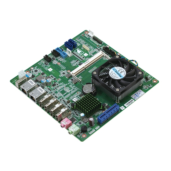
- Page 1 M i n i - I T X E M B - A 7 0 M EMB-A70M AMD R-460L(Quad-core)/ R-260H (Dual-core) APU Mini-ITX 2 Realtek 8111E Ethernet 2 USB3.0, 5 USB2.0, 2 COM 1 PCI-e, 1 Mini PCI-e 1 mSATA EMB-A70M Manual 1 August 2013...
-
Page 2: Copyright Notice
AAEON assumes no liabilities resulting from errors or omissions in this document, or from the use of the information contained herein. AAEON reserves the right to make changes in the product design without notice to its users. - Page 3 M i n i - I T X E M B - A 7 0 M Acknowledgments All other products’ name or trademarks are properties of their respective owners. Award is a trademark of Award Software International, Inc. CompactFlash is a trademark of the Compact Flash ™...
-
Page 4: Packing List
1 1702151201 SATA Power CABLE 1 M20A70M000 I/O Shield 1 17592A70M1 CPU Cooler 1 Utility DVD 1 EMB-A70M If any of these items should be missing or damaged, please contact your distributor or sales representative immediately. -
Page 5: Table Of Contents
M i n i - I T X E M B - A 7 0 M Contents Chapter 1 General Information 1.1 Introduction..............1-2 1.2 Features ..............1-3 1.3 Specifications ............1-4 Chapter 2 Quick Installation Guide 2.1 Safety Precautions ..........2-2 2.2 Location of Connectors and Jumpers ...... - Page 6 M i n i - I T X E M B - A 7 0 M Chapter 3 AMI BIOS Setup 3.1 System Test and Initialization........3-2 3.2 AMI BIOS Setup ............3-3 Chapter 4 Driver Installation 4.1 Installation………………………………………..……..4-3 Appendix A Programming The Watchdog Timer A.1 Watchdog Timer Initial Program .......A-2 Appendix B I/O Information...
-
Page 7: Chapter 1 General Information
M i n i - I T X E M B - A 7 0 M Chapter General Information 1- 1 Chapter 1 General Information... -
Page 8: Introduction
512MB. EMB-A70M has an integrated AMD Radeon™ HD7 Series graphics engine, up to 1920 x 1200 for HDMI output resolutions. With all of its integrated features, the EMB-A70M strikes a balance of performance and price. This versatile product targets Industrial Automation, Entertainment, Networking, KIOSK/POS, Transportation, Banking, Healthcare and Digital Signage applications that require high performance and high reliability. -
Page 9: Features
M i n i - I T X E M B - A 7 0 M 1.2 Features AMD R-Series APU FP2 Processor AMD Hudson M3/A70M 204-pin SODIMM x 2 DDR3 1333/1066MHz up to 8 GB Realtek 8111E for Gigabit LAN, RJ-45 x 2 ... -
Page 10: Specifications
M i n i - I T X E M B - A 7 0 M 1.3 Specifications System Processor AMD R-260H (Dual-core) and optional R-460L (Quad core) APU System Memory 2 x SoDIMM, DDR3 1333/1066 Non-ECC,Un-buffered Memory, Max. - Page 11 M i n i - I T X E M B - A 7 0 M Battery Lithium battery Power Requirement 2 x 2pin 12V ATX connector, 1 x CPU fan with 4-pin wafer 1 x System fan with 4-pin wafer, 1 x SATA power with 4-pin wafer, 1x power button switch (optional reserve)
- Page 12 M i n i - I T X E M B - A 7 0 M Audio Mic-in x 1, Line-out x 1 (on Rear I/O) USB 2.0 x 1 with Type A Connectors; USB 3.0 x 2, USB 2.0 x 4 with Pin Headers ...
-
Page 13: Chapter 2 Quick Installation Guide
M i n i - I T X E M B - A 7 0 M Chapter Quick Installation Guide 2 - 1 Chapter 2 Quick Installation Guide... -
Page 14: Safety Precautions
M i n i - I T X E M B - A 7 0 M 2.1 Safety Precautions Always completely disconnect the power cord from your board whenever you are working on it. Do not make connections while the power is on, because a sudden rush of power can damage sensitive electronic components. -
Page 15: Location Of Connectors And Jumpers
M i n i - I T X E M B - A 7 0 M 2.2 Location of Connectors and Jumpers Component Side 2 - 3 Chapter 2 Quick Installation Guide... - Page 16 M i n i - I T X E M B - A 7 0 M Solder Side 2 - 4 Chapter 2 Quick Installation Guide...
-
Page 17: Mechanical Drawing
M i n i - I T X E M B - A 7 0 M 2.3 Mechanical Drawing Component Side 2 - 5 Chapter 2 Quick Installation Guide... - Page 18 M i n i - I T X E M B - A 7 0 M Solder Side 2 - 6 Chapter 2 Quick Installation Guide...
-
Page 19: List Of Jumpers
M i n i - I T X E M B - A 7 0 M 2.4 List of Jumpers The board has a number of jumpers that allow you to configure your system to suit your application. The table below shows the function of each of the board's jumpers: Label Function Auto Power Button Selection... - Page 20 M i n i - I T X E M B - A 7 0 M CN12 KB/MS Pin Header CN14 CPU FAN Connector CN15 CPU FAN Connector (Optional) CN16 SATA Signal Connector CN17 SATA Signal Connector CN18 SATA Power Connector CN19 Dual USB3.0 Box Header CN20...
-
Page 21: Setting Jumpers
M i n i - I T X E M B - A 7 0 M 2.6 Setting Jumpers You configure your card to match the needs of your application by setting jumpers. A jumper is the simplest kind of electric switch. It consists of two metal pins and a small metal clip (often protected by a plastic cover) that slides over the pins to connect them. -
Page 22: Auto Power Button Setting (Cn8)
M i n i - I T X E M B - A 7 0 M 2.7 Auto Power Button Setting (CN8) Function Normal (Default) Auto Button 2.8 COM1 RI Power Selection (CN9) Function Normal (Default) 2.9 CMOS Setting (CN22) Function Normal (Default) Clear CMOS... -
Page 23: Digital I/O Pin Header (Dio1)
M i n i - I T X E M B - A 7 0 M USBD2- A_JD_FRONT LINE2_L LINE IN SENSOR resister 2.12 RS232 /422/485 Pin Header (COM1) Signal Signal 2.13 Digital I/O Pin Header (DIO1) Signal Signal DIO1 DIO2 DIO3 DIO4... -
Page 24: Sata Connector (Sata 1~5)
M i n i - I T X E M B - A 7 0 M +12V +12V 2.16 SATA Connector (SATA 1~5) Signal Signal 2.17 USB3.0 Connector (USB3_34) Signal Signal +5V_USB3_2_P1 +5V_USB3_2_P2 U3_2_U3RXDN1 U3_2_U3RXDN2 U3_2_U3RXDP1 U3_2_U3RXDP2 U3_2_U3TXDN1 U3_2_U3TXDN2 U3_2_U3TXDP1 U3_2_U3TXDP2 U3_2_U2DN1 U3_2_U2DN2... - Page 25 M i n i - I T X E M B - A 7 0 M Below Table for China RoHS Requirements 产品中有毒有害物质或元素名称及含量 AAEON Main Board/ Daughter Board/ Backplane 有毒有害物质或元素 部件名称 铅 汞 镉 六价铬 多溴联苯 多溴二苯醚 (Pb) (Hg) (Cd)
- Page 26 M i n i - I T X E M B - A 7 0 M Chapter BIOS Setup Chapter 3 AMI BIOS Setup 3-1...
- Page 27 4. The CMOS memory has lost power and the configuration information has been erased. The EMB-A70M CMOS memory has an integral lithium battery backup for data retention. However, you will need to replace the complete unit when it finally runs down.
-
Page 28: Chapter 3 Ami Bios Setup
M i n i - I T X E M B - A 7 0 M 3.2 AMI BIOS Setup AMI BIOS ROM has a built-in Setup program that allows users to modify the basic system configuration. This type of information is stored in battery-backed CMOS RAM and BIOS NVRAM so that it retains the Setup information when the power is turned off. -
Page 29: Setup Menu
M i n i - I T X E M B - A 7 0 M Setup Menu Setup submenu: Main Chapter 3 AMI BIOS Setup 3-4... - Page 30 M i n i - I T X E M B - A 7 0 M Setup submenu: Advanced Chapter 3 AMI BIOS Setup 3-5...
-
Page 31: Acpi Settings
M i n i - I T X E M B - A 7 0 M ACPI Settings Options summary: ACPI Sleep State S3 only (Suspend to RAM) Optimal Default, Failsafe Default Select the ACPI state used for System Suspend Chapter 3 AMI BIOS Setup 3-6... -
Page 32: Cpu Configuration
M i n i - I T X E M B - A 7 0 M CPU Configuration Chapter 3 AMI BIOS Setup 3-7... - Page 33 M i n i - I T X E M B - A 7 0 M IDE Configuration (IDE) Options summary: OnChip SATA RAID Type AHCI Optimal Default, Failsafe Default Legacy IDE Chapter 3 AMI BIOS Setup 3-8...
-
Page 34: Usb Configuration
M i n i - I T X E M B - A 7 0 M USB Configuration Options summary: Legacy USB Support Enabled Optimal Default, Failsafe Default Disabled Auto Enables BIOS Support for Legacy USB Support. When enabled, USB can be functional in legacy environment like DOS. -
Page 35: Super Io Configuration
M i n i - I T X E M B - A 7 0 M Super IO Configuration Chapter 3 AMI BIOS Setup 3-10... -
Page 36: Serial Port 1 Configuration
M i n i - I T X E M B - A 7 0 M Serial Port 1 Configuration Options summary: Serial Port Disabled Enabled Optimal Default, Failsafe Default Allows BIOS to En/Disable correspond serial port. Change Settings Auto Optimal Default, Failsafe Default IO=3F8h;IRQ=4;... -
Page 37: Serial Port 2 Configuration
M i n i - I T X E M B - A 7 0 M Serial Port 2 Configuration Options summary: Serial Port Disabled Enabled Optimal Default, Failsafe Default Allows BIOS to En/Disable correspond serial port. Change Settings Auto Optimal Default, Failsafe Default IO=3F8h;IRQ=4;... - Page 38 M i n i - I T X E M B - A 7 0 M H/W Monitor Chapter 3 AMI BIOS Setup 3-13...
- Page 39 M i n i - I T X E M B - A 7 0 M Smart Fan Mode Configuration (Manual Mode) Options Summary : CPU Fan Control Disabled (SYS Fan Control) Enabled Default For En/Disable CPU(SYS) Fan1 Control Enabled: Fan is running in accordance with user settings Disabled: Fan is always running with full speed Fan Control Mode...
- Page 40 M i n i - I T X E M B - A 7 0 M Smart Fan Mode Configuration (Thermal Cruise Mode) Options Summary : Spin PWM Default The PWM Duty of Fan Spin Off Control Default Temperature Temperature Limit Value of Fan Off. Note: Some fans have the minimum speed even if the PWM value is 0 Start Control Default...
- Page 41 M i n i - I T X E M B - A 7 0 M Dynamic Digital IO Options summary: GPI0~GPI3 Input Optimal Default, Failsafe Default Direction Output Set GPIO as Input or Output GPO0~GPI3 Input Direction Output Optimal Default, Failsafe Default Set GPIO as Input or Output Output Level Optimal Default, Failsafe Default...
-
Page 42: Trusted Computing
M i n i - I T X E M B - A 7 0 M Trusted Computing Options summary: Security Device Disabled Optimal Default, Failsafe Default Support Enabled Enable/Disable Security Device. NOTE: Your Computer will reboot during restart in order to change State of the Device. -
Page 43: Power Management
M i n i - I T X E M B - A 7 0 M Power Management Options summary: Power Mode ATX Type Optimal Default, Failsafe Default AT Type Select power supply mode. Resume from RI Disabled Enabled Optimal Default, Failsafe Default Enable/Disable Resume from RI Chapter 3 AMI BIOS Setup 3-18... - Page 44 M i n i - I T X E M B - A 7 0 M S5 RTC Wake Settings (Fixed Time) Options summary: Wake system with Disabled Optimal Default, Failsafe Default Fixed Time Enabled En/Disable System wake on alarm event. When enabled, System will wake on the hr:min:sec specified Wake up day 0-31...
- Page 45 M i n i - I T X E M B - A 7 0 M S5 RTC Wake Settings (Dynamic Time) Options summary: Wake system with Disabled Optimal Default, Failsafe Default Dynamic Time Enabled En/Disable System wake on alarm event. When enabled, System will wake on current time + Increases minutese(s) Wake up day Default 1...
- Page 46 M i n i - I T X E M B - A 7 0 M Setup submenu: Chipset Chapter 3 AMI BIOS Setup 3-21...
-
Page 47: Host Bridge
M i n i - I T X E M B - A 7 0 M HOST Bridge Chapter 3 AMI BIOS Setup 3-22... -
Page 48: South Bridge
M i n i - I T X E M B - A 7 0 M South Bridge Options summary: HD Audio Azalia Auto Device Disabled Optimal Default, Failsafe Default Enabled Control Detection of the Azalia device.\n\nDisabled = Azalia will be unconditionally disabled\n\nEnabled = Azalia will be unconditionally Enabled GPP Port Link x4 mode... - Page 49 M i n i - I T X E M B - A 7 0 M Setup submenu: Boot Chapter 3 AMI BIOS Setup 3-24...
- Page 50 M i n i - I T X E M B - A 7 0 M Options summary: Bootup NumLock State Default Select the keyboard NumLock state Quiet Boot Disabled Enabled Default En/Disable showing boot logo. Launch I82579LM PXE Disabled Default OpROM Enabled...
- Page 51 M i n i - I T X E M B - A 7 0 M BBS Priorities Chapter 3 AMI BIOS Setup 3-26...
- Page 52 M i n i - I T X E M B - A 7 0 M Security Change User/Supervisor Password You can install a Supervisor password, and if you install a supervisor password, you can then install a user password. A user password does not provide access to many of the features in the Setup utility.
- Page 53 M i n i - I T X E M B - A 7 0 M Setup submenu: Exit Chapter 3 AMI BIOS Setup 3-28...
-
Page 54: Chapter 4 Driver Installation
M i n i - I T X E M B - A 7 0 M Chapter Driver Installation 4 -1 Chapter 4 Driver Installation... - Page 55 M i n i - I T X E M B - A 7 0 M The EMB-A70M comes with an Autorun DVD-ROM that contains all drivers and utilities that can help you to install the driver automatically. Insert the driver DVD, the driver DVD-title will automatically start and show the installation guide.
- Page 56 M i n i - I T X E M B - A 7 0 M 4.1 Installation: Insert the EMB-A70M DVD-ROM into the DVD-ROM drive. And install the drivers from Step 1 to Step 6 in order. Step 1 – Install Chipset & VGA Driver 1.
- Page 57 M i n i - I T X E M B - A 7 0 M 3. Follow the instructions that the window shows 4. The system will help you install the driver automatically Step 5 – Install TPM Driver 1.
- Page 58 M i n i - I T X E M B - A 7 0 M 2. Change User Account Control Settings to [Never notify] 4 -5 Chapter 4 Driver Installation...
- Page 59 M i n i - I T X E M B - A 7 0 M 3. Reboot and Administrator login. 4. To run patch.bat with [Run as administrator]. 4 -6 Chapter 4 Driver Installation...
-
Page 60: Appendix A Programming The Watchdog Timer
M i n i - I T X E M B - A 7 0 M Appendix Programming the Watchdog Timer Appendix A Programming the Watchdog Timer A-1... -
Page 61: Watchdog Timer Initial Program
M i n i - I T X E M B - A 7 0 M A.1 Watchdog Timer Initial Program Table 1 : SuperIO relative register table Default Value Note SIO MB PnP Mode Index Register Index 0x2E (Note1) 0x2E or 0x4E SIO MB PnP Mode Data Register Data 0x2F (Note2) 0x2F or 0x4F Table 2 : Watchdog relative register table LDN Register ... - Page 62 M i n i - I T X E M B - A 7 0 M ************************************************************************************ // SuperIO relative definition (Please reference to Table 1) #define byte SIOIndex //This parameter is represented from Note1 #define byte SIOData //This parameter is represented from Note2 #define void IOWriteByte(byte IOPort, byte Value); #define byte IOReadByte(byte IOPort); // Watch Dog relative definition (Please reference to Table 2) #define byte TimerLDN //This parameter is represented from Note3 #define byte ...
- Page 63 M i n i - I T X E M B - A 7 0 M ************************************************************************************ Main VOID (){ // Procedure : AaeonWDTConfig // (byte)Timer : Time of WDT timer.(0x00~0xFF) // (boolean)Unit : Select time unit(0: second, 1: minute). AaeonWDTConfig(); // Procedure : AaeonWDTEnable // This procudure will enable the WDT counting. AaeonWDTEnable(); } ************************************************************************************ Appendix A Programming the Watchdog Timer A-4...
- Page 64 M i n i - I T X E M B - A 7 0 M ************************************************************************************ // Procedure : AaeonWDTEnable AaeonWDTEnable () VOID { WDTEnableDisable( ); EnableLDN, EnableReg, EnableBit, 1 } // Procedure : AaeonWDTConfig AaeonWDTConfig () VOID { // Disable WDT counting WDTEnableDisable( ); EnableLDN, EnableReg, EnableBit, 0 // Clear Watchdog Timeout Status WDTClearTimeoutStatus(); // WDT relative parameter setting WDTParameterSetting(); } ...
- Page 65 M i n i - I T X E M B - A 7 0 M ************************************************************************************ SIOEnterMBPnPMode() VOID { Switch(SIOIndex){ Case 0x2E: IOWriteByte(SIOIndex, 0x87); IOWriteByte(SIOIndex, 0x01); IOWriteByte(SIOIndex, 0x55); IOWriteByte(SIOIndex, 0x55); Break; Case 0x4E: ...
- Page 66 M i n i - I T X E M B - A 7 0 M ************************************************************************************ SIOBitSet(byte LDN, byte Register, byte BitNum, byte Value) VOID { Byte TmpValue; SIOEnterMBPnPMode(); SIOSelectLDN(byte ); IOWriteByte(SIOIndex, Register); TmpValue = IOReadByte(SIOData); TmpValue &= ~(1 << BitNum); TmpValue |= (Value << BitNum); IOWriteByte(SIOData, TmpValue); SIOExitMBPnPMode(); } ...
-
Page 67: Appendix B I/O Information
M i n i - I T X E M B - A 7 0 M Appendix I/O Information Appendix B I/O Information... -
Page 68: I/O Address Map
M i n i - I T X E M B - A 7 0 M B.1 I/O Address Map Appendix B I/O Information... - Page 69 M i n i - I T X E M B - A 7 0 M Appendix B I/O Information...
- Page 70 M i n i - I T X E M B - A 7 0 M Appendix B I/O Information...
-
Page 71: Memory Address Map
M i n i - I T X E M B - A 7 0 M B.2 Memory Address Map Appendix B I/O Information... -
Page 72: Irq Mapping Chart
M i n i - I T X E M B - A 7 0 M B.3 IRQ Mapping Chart Appendix B I/O Information... - Page 73 M i n i - I T X E M B - A 7 0 M Appendix B I/O Information...
- Page 74 M i n i - I T X E M B - A 7 0 M Appendix B I/O Information...
- Page 75 M i n i - I T X E M B - A 7 0 M Appendix B I/O Information...
-
Page 76: Dma Channel Assignments
M i n i - I T X E M B - A 7 0 M B.4 DMA Channel Assignments B-10 Appendix B I/O Information... - Page 77 M i n i - I T X E M B - A 7 0 M Appendi Mating Connecotor C - 1 Appendix C Mating Connector...
-
Page 78: Appendix C Mating Connector
M i n i - I T X E M B - A 7 0 M C.1 List of Mating Connectors and Cables The table notes mating connectors and available cables. Connector Function Mating Connector Available Cable AAEON Cable Label Vendor Model no HO-BASE.K CN32 Upright... - Page 79 161S01-029 CN17 SATA Cable 1709070150 Connector 1130-010-08 凱迅 CN12 Connector 1190-700-04 CATCH Connector POWER 何迪 CN18 P201-04 Connector Note: The AAEON Cable P/N with “ * ” sign is for WiTAS series products. C - 3 Appendix C Mating Connector...
- Page 80 M i n i - I T X E M B - A 7 0 M A ppendix Programming the Digital I/O Appendix D Electrical Specifications for I/O Ports...
-
Page 81: Dio Programming
M i n i - I T X E M B - A 7 0 M D.1 DIO Programming EMB-A70M utilizes ITE8728 chipset as its Digital I/O controller. Below are the procedures to complete its configuration which you can develop customized program to fit your application. -
Page 82: Digital I/O Register
M i n i - I T X E M B - A 7 0 M D.2 Digital I/O Register Table 1 : Digital I/O relative register table Register DIO access Base Address 0x500 (Note3) Register BitNum Value Note DIO‐1 Pin Status Base Address+0 GPIO11 (Note4) (Note5) (Note6) DIO‐2 Pin Status Base Address+0 GPIO12 (Note7) (Note8) -
Page 83: Digital I/O Sample Program
M i n i - I T X E M B - A 7 0 M D.3 Digital I/O Sample Program ************************************************************************************ #define void IOWriteByte(byte IOPort, byte Value); #define byte IOReadByte(byte IOPort); // Digital Input Status relative definition (Please reference to Table 1) #define byte DIOBaseAddress // This parameter is represented from Note3 #define byte DIO1Reg // This parameter is represented from Note4 #define byte ... - Page 84 M i n i - I T X E M B - A 7 0 M ************************************************************************************ Main VOID (){ Boolean PinStatus ; // Procedure : AaeonReadPinStatus // Input : // Example, Read Digital I/O Pin 3 status // Output : // InputStatus : // 0: Digital I/O Pin level is low // 1: Digital I/O Pin level is High ...
- Page 85 M i n i - I T X E M B - A 7 0 M ************************************************************************************ AaeonReadPinStatus(byte Register, byte BitNum) Boolean { Boolean PinStatus ; PinStatus = DIOBitRead(Register, BitNum); Return PinStatus ; } AaeonSetOutputLevel(byte Register, byte BitNum, byte Value) VOID { DIOBitSet(Register, BitNum, Value); } DIOBitRead(byte Register, byte BitNum) Boolean { ...
-
Page 86: Appendix E Ahci Setting
M i n i - I T X E M B - A 7 0 M Appendix AHCI Setting Appendix E AHCI Setting... -
Page 87: Setting Ahci
M i n i - I T X E M B - A 7 0 M E.1 Setting AHCI OS installation to setup AHCI Mode Step 1: Copy the files below from “Driver CD ->Step 2 – AHCI_RAID -> Floppy -> WinXP -> 3.3.1540.26 -> x86” to Disk Step 2: Connect the USB Floppy (disk with RAID files) to the board Appendix E AHCI Setting... - Page 88 M i n i - I T X E M B - A 7 0 M Step 3: The setting procedures “ In BIOS Setup Menu” A: Advanced -> SATA Configuration -> SATA Configuration -> SATA Mode -> AHCI Mode Step 4: The setting procedures “In BIOS Setup Menu”...
- Page 89 M i n i - I T X E M B - A 7 0 M Step 5: The setting procedures “In BIOS Setup Menu” C: Save & Exit -> Save Changes and Exit Step 6: Setup OS Appendix E AHCI Setting...
- Page 90 M i n i - I T X E M B - A 7 0 M Step 7: Press “F6” Step 8: Choose “S” Appendix E AHCI Setting...
- Page 91 M i n i - I T X E M B - A 7 0 M Step 9: Choose “Intel(R) 5 Series 6 Port SATA AHCI Controller” tep 10: It will show the model number you select and then press “ENTER” Appendix E AHCI Setting...
- Page 92 M i n i - I T X E M B - A 7 0 M Step 11: Setup is loading files Appendix E AHCI Setting...
Need help?
Do you have a question about the EMB-A70M and is the answer not in the manual?
Questions and answers