Tektronix DSA8300 Technical Reference
Digital serial analyzer, sampling modules, accessory modules, performance verification
Hide thumbs
Also See for DSA8300:
- Programmer's manual (455 pages) ,
- Service manual (138 pages) ,
- Quick start user manual (108 pages)

Related Manuals for Tektronix DSA8300


Summary of Contents for Tektronix DSA8300
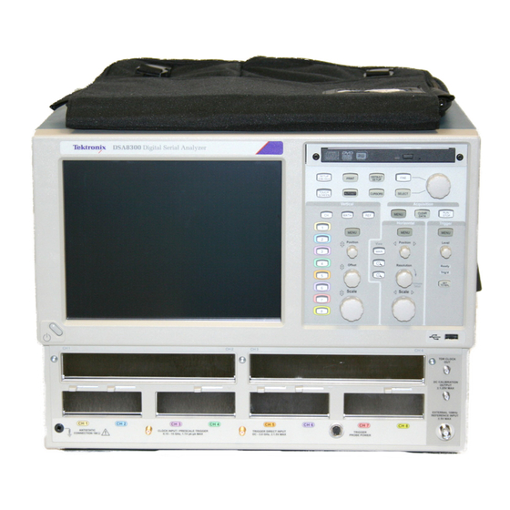
- Page 1 DSA8300 Digital Serial Analyzer 80C00, 80E00 Sampling Modules 80A00 Accessory Modules Performance Verification Technical Reference *P077068203* 077-0682-03...
-
Page 3: Technical Reference
DSA8300 Digital Serial Analyzer 80C00, 80E00 Sampling Modules 80A00 Accessory Modules Performance Verification Technical Reference Warning The servicing instructions are for use by qualified personnel only. To avoid personal injury, do not perform any servicing unless you are qualified to do so. Refer to all safety summaries prior to performing service. - Page 4 Copyright © Tektronix. All rights reserved. Licensed software products are owned by Tektronix or its subsidiaries or suppliers, and are protected by national copyright laws and international treaty provisions. Tektronix products are covered by U.S. and foreign patents, issued and pending. Information in this publication supersedes that in all previously published material.
- Page 5 Tektronix, with shipping charges prepaid. Tektronix shall pay for the return of the product to Customer if the shipment is to a location within the country in which the Tektronix service center is located. Customer shall be responsible for paying all shipping charges, duties, taxes, and any other charges for products returned to any other locations.
- Page 7 Performance Tests ....................Prerequisites ....................Equipment Required..................DSA8300 Digital Serial Analyzer Test Records ............DSA8300 Main Instrument and 82A04 Module Test Record..........80E00 Electrical Modules Test Record..............80C00 Test Records ..................80A02 EOS/ESD Protection Module Test Record ............80A05 Electrical Clock Recovery Module Test Record..........
- Page 8 Clock Recovery Optical Sensitivity Range and Recovered Clock Timing Jitter ....80A02 EOS/ESD Protection Module................Prerequisites ....................Logic Control Threshold ................... 80A05 Electrical Clock Recovery Module ..............Prerequisites ....................Clock Recovery Sensitivity Range and Recovered Clock Timing Jitter......DSA8300 Performance Verification...
- Page 9 Figure 36: Display example (clock signal synchronized with the data rate input) ....... Figure 37: Display example (zoomed in at the crossing point)..........Figure 38: 80A02 test setup ..................Figure 39: Clock recovery sensitivity range and recovered clock timing jitter setup....DSA8300 Performance Verification...
- Page 10 Table of Contents Figure 40: Display example (clock signal synchronized with the data rate input) ....... Figure 41: Display example (zoomed in at the crossing point)..........DSA8300 Performance Verification...
- Page 11 Table 10: Minimum limits..................Table 11: Aberrations ................... Table 12: Clock recovery settings ................Table 13: Clock recovery settings and jitter limits............Table 14: Clock recovery settings ................Table 15: Clock recovery amplitude and jitter limits ............DSA8300 Performance Verification...
-
Page 12: Important Safety Information
To avoid electric shock, the grounding conductor must be connected to earth ground. Before making connections to the input or output terminals of the product, make sure that the product is properly grounded. DSA8300 Performance Verification... - Page 13 Use only insulated voltage probes, test leads, and adapters supplied with the product, or indicated by Tektronix to be suitable for the product. Observe all terminal ratings. To avoid fire or shock hazard, observe all ratings and markings on the product.
- Page 14 The product is heavy. To reduce the risk of personal injury or damage to the device, get help when lifting or carrying the product. Use only the Tektronix rackmount hardware specified for this product. Service safety summary The Service safety summary section contains additional information required to safely perform service on the product.
- Page 15 find out the nature of the potential hazards and any actions which have to be taken to avoid them. (This symbol may also be used to refer the user to ratings in the manual.) The following symbol(s) may appear on the product: DSA8300 Performance Verification...
- Page 16 Important safety information DSA8300 Performance Verification...
- Page 17 Preface This manual contains the specifications and performance verification procedures for the DSA8300 Digital Serial Analyzer, the extender cables, and the modules that can be installed in this instrument (except the 80A03 module). NOTE. The 80A03 instruction manual contains its own specifications and servicing information.
- Page 18 Preface Related Documentation The following documents relate to the instrument this manual supports: DSA8300 Digital Serial Analyzer Quick Start User Manual. Tektronix part number 071-2897-XX. DSA8300 Digital Serial Analyzer Service Manual. Tektronix part number 071-2049-XX. DSA8300 Digital Serial Analyzer Online Help. Installed with the application software and accessed from the instrument Help menu.
-
Page 19: Performance Verification Procedures
They require more time to perform and suitable test equipment is required. (See page 17, Equipment Required.) If you are not familiar with operating this instrument, refer to the online help or the user information supplied with the instruments. DSA8300 Performance Verification... -
Page 20: Functional Test Procedures
Functional Test Procedures Functional Test Procedures There are three procedures in this section that provide a quick way to confirm basic functionality and proper adjustment of the DSA8300: (See page 2, Instrument Diagnostics.) (See page 3, Instrument and Module Compensation.) (See page 6, Instrument Functional Tests.) -
Page 21: Instrument And Module Compensation
Performing a vertical compensation will maximize the accuracy of the automatic measurements you take. This procedure uses internal routines to optimize the vertical offset, gain, and linearity. A complete compensation requires running separate compensations on the mainframe and the modules. DSA8300 Performance Verification... - Page 22 Functional Test Procedures Equipment required For sampling modules: 50 Ω terminations on all electrical module channels (Tektronix part number 015-1022-xx). Dust covers on all optical module channels. The sampling modules ship from Tektronix with the proper terminations and dust covers installed.
- Page 23 (use the Utilities > View/Change Module Config tool, available on TekScope SW version 6.0.124 and greater to move the module while the instrument is DSA8300 Performance Verification...
-
Page 24: Instrument Functional Tests
Equipment required One coaxial SMA cable, 50 Ω, 20 in (0.5 m), male-to-male (item Channels Prerequisites One electrical sampling module (80E01, 80E02, 80E03, 80E04, 80E06, 80E07B, 80E08B, 80E09B, or 80E10B) Figure 1: Setup for electrical functional tests DSA8300 Performance Verification... -
Page 25: Figure 2: Channel Button Location
Push the front-panel Vertical MENU button again to dismiss the Vert Setup dialog box. 5. Push the channel button for the channel to test. The button lights and the screen shows the selected channel signal. Figure 2: Channel button location DSA8300 Performance Verification... - Page 26 first row of the following table that applies to your module model. d. Confirm that the Mean measurement readout value for the channel under test is within the limits shown in the table. e. Repeat steps c and d for each row in the table for your module. DSA8300 Performance Verification...
- Page 27 600.0 600.0 594.6 605.4 10. Test all channels: Repeat steps 3 through 9 until all input channels are verified. 11. Remove the test setup: Disconnect the SMA cable from the channel input and the DC CALIBRATION output. DSA8300 Performance Verification...
-
Page 28: Figure 3: Channel Button Location
4. Verify that the channel is operational: Confirm that the following statements are true. A trace displays at about center screen. The Waveform readout for the channel under test shows a value as follows: 80C01, 80C02, 80C04, 80C09, 80C11, and 80C11B: 1 mW 80C03: 100 μW DSA8300 Performance Verification... - Page 29 Equipment required One SMA cable, 50 Ω, 20 in (0.5 m), male-to-male connectors (item 15) One 10x SMA attenuator (item 56) One electrical sampling module (80E01, 80E02, 80E03, 80E04, 80E06, 80E07B, 80E08B, 80E09B, or 80E10B) Prerequisites None DSA8300 Performance Verification...
-
Page 30: Figure 4: Setup For The Time Base Tests
Rotate the vertical OFFSET knob counterclockwise so that the base of the square wave is about 2 divisions below the center graticule. This is to ensure that a vertical trace will be seen for rise and fall. DSA8300 Performance Verification... - Page 31 (about 10 horizontal divisions per waveform period); rotating the Horizontal SCALE knob counterclockwise returns the Horizontal scale setting to 1 μs/div returns the waveform period to about five divisions. Leave the Horizontal Scale set to 1 μs/div. DSA8300 Performance Verification...
-
Page 32: Figure 5: Mag Time Base Verification
Prerequisites The instrument must be powered on and running. Power on the instrument and verify that you can feel airflow from all six cooling fans on the left side of the instrument. End of Functional Test Procedures DSA8300 Performance Verification... -
Page 33: Performance Tests
(See page 177, DC Voltage Measurement Accuracy.) Perform this check for each channel of each small-module slot. Be sure to run the instrument compensation routine with the tested module installed each time you move the module to a new slot. DSA8300 Performance Verification... -
Page 34: Prerequisites
20 minutes, and must be operating at an ambient temperature. Observe all safety rules, especially regarding voltage hazards. These procedures cover all instrument models. Please ignore checks that do not apply to the specific model you are testing. DSA8300 Performance Verification... -
Page 35: Equipment Required
Equipment Required The procedures mentioned in Main Instruments section use external, traceable signal sources to directly check warranted characteristics. (See page 151, DSA8300 Performance Verification.) The following table lists the required equipment. WARNING. Some of the generator equipment used to complete the performance tests may be capable of producing dangerous output levels. - Page 36 Item number and description Minimum requirements Part number or model Cable, coaxial (Qty. 2) 50 Ω, 20 in (0.5 m), male-to-male Tektronix part number 174-1427-00 SMA connectors Tektronix part number 174-1341-00 Cable, coaxial 50 Ω, 39.37 in (1.0 m), male-to-male SMA connectors 50 Ω, 60 in (1.5 m), male-to-male...
- Page 37 6 dB attenuator, DC to 50 GHz, 80E09B, and 80E10B only) (Qty. 2) 2.4 mm connectors Electrical sampling module extender Extender cable for use with certain Tektronix 80N01 or 80X02 Module cable (2 meter) small compartment modules Extender Cable Attenuator (80A05 only) (Qty. 2)
-
Page 38: Dsa8300 Digital Serial Analyzer Test Records
DSA8300 Digital Serial Analyzer Test Records This section contains test records that you can use to record the results of your performance verification checks. DSA8300 Main Instrument (includes 82A04 Phase Reference module) 80E00 Electrical Sampling Modules 80C00 Optical Sampling Modules... -
Page 39: Dsa8300 Main Instrument And 82A04 Module Test Record
Performance Tests DSA8300 Main Instrument and 82A04 Module Test Record For each channel tested, print this record and enter the performance test results for your main-instrument test record. DSA8300 and 82A04 Test Record for Channel Instrument Serial Number: Cal Certificate Number:... - Page 40 Performance Tests Minimum Incoming Maximum DSA8300 and 82A04 Performance Test Outgoing DC Calibration Output Set to: +1.0 V +0.9988 V +1.0012 V 0.0 V –0.2 mV +0.2 mV –1.0 V –1.0012 V –0.9988 V 29 ns for 80E07B, 80E08B, 80E09B, 80E10B...
-
Page 41: E00 Electrical Modules Test Record
80E02 Baseline (80E04 only) –1 mV 1 mV 80E03 Impedance 49.5 Ω 50.5 Ω 80E04 80E06 Baseline (80E04 only) –1 mV 1 mV 80E07B Impedance 49 Ω 51 Ω 80E08B Impedance 49 Ω 51 Ω 80E09B 80E10B DSA8300 Performance Verification... - Page 42 +1100 mV -18.7 mV +18.7 mV +850 mV +1100 mV -14.7 mV +14.7 mV +1100 mV +1100 mV -9.7 mV +9.7 mV +1350 mV +1100 mV -14.7 mV +14.7 mV +1550 mV +1100 mV -18.7 mV +18.7 mV DSA8300 Performance Verification...
- Page 43 +600 mV -15.2 mV +15.2 mV +350 mV +600 mV -11.2 mV +11.2 mV +600 mV +600 mV -6.2 mV +6.2 mV +850 mV +600 mV -11.2 mV +11.2 mV +1050 mV +600 mV -15.2 mV +15.2 mV DSA8300 Performance Verification...
- Page 44 Vert scale: 1 mV 410 μV 80E08B none C2 (BW 30 GHz) Vert scale: 1 mV 410 μV none C1 (BW 20 GHz) Vert scale: 1 mV 380 μV none Vert scale: 1 mV 380 μV C2 (BW 20 GHz) DSA8300 Performance Verification...
- Page 45 C1 (to 60 GHz) Max power +3 dB (50 MHz ref) Min power -3 dB (50 MHz ref) none C2 (to 60 GHz) Max power +3 dB (50 MHz ref) Min power -3 dB (50 MHz ref) DSA8300 Performance Verification...
- Page 46 TDR system step response aberrations (80E04, 80E08B, 80E10B models only) 80E04 C1 positive polarity zone: from -10 ns to -20 ps zone: from 400 ps to 5 ns zone: from 5 ns C1 negative polarity zone: from -10 ns to -20 ps DSA8300 Performance Verification...
- Page 47 +12% 150 ps to 400 ps zone: from 400 ps to 5 ns zone: from 5 ns to 100 ns zone: from 100 ns to end C2 positive polarity zone: from -10 ns to -20 ps DSA8300 Performance Verification...
- Page 48 -10 ns to -20 ps zone: from 14 ps +25% to 150 ps zone: from +12% 150 ps to 400 ps zone: from 400 ps to 5 ns zone: from 5 ns to 100 ns zone: from 100 ns to end DSA8300 Performance Verification...
- Page 49 150 ps zone: from +12% 150 ps to 400 ps zone: from 400 ps to 5 ns zone: from 5 ns to 100 ns zone: from 100 ns to end Before step transition. After step transition. DSA8300 Performance Verification...
-
Page 50: C00 Test Records
(See page 100, 80C12 Test Record.) (See page 104, 80C12-10G Test Record.) (See page 109, 80C12B Test Record.) (See page 126, 80C12B-10G Test Record.) (See page 134, 80C14 Test Record.) (See page 144, 80C15 Test Record.) (See page 146, 80C25BGE Test Record.) DSA8300 Performance Verification... - Page 51 +0.50 93.3 –0.11 –0.61 +0.39 186.6 –0.45 –0.95 +0.05 279.9 –1.02 –1.52 –0.52 373.2 –1.86 –2.36 –1.36 466.7 –3.00 –3.50 –2.50 559.9 –4.51 –5.67 –3.35 622.1 –5.71 –7.25 –4.17 653.2 –6.37 –8.08 –4.66 746.5 –8.54 –10.74 –6.35 DSA8300 Performance Verification...
- Page 52 10451.2 –6.37 –8.75 –3.99 11944.0 –8.54 –11.53 –5.56 13437.2 –10.93 –14.45 –7.41 14930.4 –13.41 –17.41 –9.41 Recovered clock timing jitter (80C01-CR only) Rate Horz scale none OC-12 500 ps 8 ps none OC-48 100 ps 8 ps DSA8300 Performance Verification...
- Page 53 +0.40 4478.8 –1.02 –1.87 +0.17 5972.4 –1.86 –2.71 –1.01 7465.0 –3.00 –3.86 –2.16 8958.0 –4.51 –6.19 –2.83 9953.28 –5.71 –7.87 –3.55 10451.2 –6.37 –8.75 –3.99 11944.0 –8.54 –11.53 –5.56 13437.2 –10.93 –14.45 –7.41 14930.4 –13.41 –17.41 –9.41 DSA8300 Performance Verification...
- Page 54 Performance Tests 80C02 performance test Minimum Incoming Outgoing Maximum Recovered clock timing jitter (80C02-CR only) Rate Horz scale none 20 ps 2 ps OC-192 DSA8300 Performance Verification...
- Page 55 3732.6 –13.41 –16.41 –10.41 ENET2500 (GBE) 2.50 Gb/s Reference Receiver setting frequency response (dB) Frequency (MHz) Nominal response (dB) 0.00 0.00 –0.50 +0.50 –0.11 –0.61 +0.39 –0.45 –0.95 +0.05 1125 –1.02 –1.52 –0.52 1500 –1.86 –2.36 –1.36 DSA8300 Performance Verification...
- Page 56 +0.05 478.4 –1.02 –1.52 –0.52 637.9 –1.86 –2.36 –1.36 797.4 –3.00 –3.50 –2.50 956.8 –4.51 –5.67 –3.35 1063 –5.71 –7.25 –4.17 1116 –6.37 –8.08 –4.66 1275 –8.54 –10.74 –6.35 1435 –10.93 –13.55 –8.31 1595 –13.41 –16.41 –10.41 DSA8300 Performance Verification...
- Page 57 Minimum Incoming Outgoing Maximum Recovered clock timing jitter (80C03-CR only) Rate Horz scale none 200 ps 8 ps FC1063 none 200 ps 8 ps none OC-48 100 ps 8 ps none 2.5 Gb/s 100 ps 8 ps DSA8300 Performance Verification...
- Page 58 +0.40 4478.8 –1.02 –1.87 +0.17 5972.4 –1.86 –2.71 –1.01 7465.0 –3.00 –3.86 –2.16 8958.0 –4.51 –6.19 –2.83 9953.28 –5.71 –7.87 –3.55 10451.2 –6.37 –8.75 –3.99 11944.0 –8.54 –11.53 –5.56 13437.2 –10.93 –14.45 –7.41 14930.4 –13.41 –17.41 –9.41 DSA8300 Performance Verification...
- Page 59 –6.19 –2.83 10664.0 –5.71 –7.87 –3.55 11197.5 –6.37 –8.75 –3.99 12796.9 –8.54 –11.53 –5.56 14396.7 –10.93 –14.45 –7.41 15996.5 –13.41 –17.41 –9.41 Recovered clock timing jitter (80C04-CR only) Rate Horz scale none OC-192 20 ps 2 ps DSA8300 Performance Verification...
- Page 60 +0.40 4478.8 –1.02 –1.87 +0.17 5972.4 –1.86 –2.71 –1.01 7465.0 –3.00 –3.86 –2.16 8958.0 –4.51 –6.19 –2.83 9953.28 –5.71 –7.87 –3.55 10451.2 –6.37 –8.75 –3.99 11944.0 –8.54 –11.53 –5.56 13437.2 –10.93 –14.45 –7.41 14930.4 –13.41 –17.41 –9.41 DSA8300 Performance Verification...
- Page 61 Performance Tests 80C05 performance test Minimum Incoming Outgoing Maximum Aberrations (peak-to-peak) none Filter or Bandwidth OC-192/STM-64 none 20 GHz none 30 GHz none 40 GHz DSA8300 Performance Verification...
- Page 62 Maximum Dark level (C1 at 200 μW) 50 GHz –25 μW +25 μW Vertical equivalent optical noise (C1 at 200 μW) none 50 GHz 192 μW none Clock Recovery 192 μW Aberrations (peak-to-peak) none Bandwidth 50 GHz DSA8300 Performance Verification...
- Page 63 OC-3/STM-1 1.0 μW none Clock Recovery 1.0 μW none OC-12/STM-4 1.0 μW none Clock Recovery 1.0 μW none OC-48/STM-16 1.5 μW none Clock Recovery 1.5 μW Minimum optical bandwidth none 2 GHz bandwidth setting 2.3 GHz DSA8300 Performance Verification...
- Page 64 Frequency (MHz) Nominal response (dB) 0.00 0.00 –0.50 +0.50 373.3 –0.11 –0.61 +0.39 746.5 –0.45 –0.95 +0.05 1119.7 –1.02 –1.52 –0.52 1493.1 –1.86 –2.36 –1.36 1866.3 –3.00 –3.50 –2.50 2239.5 –4.51 –5.67 –3.35 2488.3 –5.71 –7.25 –4.17 DSA8300 Performance Verification...
- Page 65 –10.74 –6.35 3359.3 –10.93 –13.55 –8.31 3732.6 –13.41 –16.41 –10.41 Recovered clock timing jitter (80C07-CR only) Rate Horz scale none OC-3 1 ns 32 ps none OC-12 500 ps 8 ps none OC-48 100 ps 4 ps DSA8300 Performance Verification...
- Page 66 ENET1250 1.0 μW none Clock Recovery 1.0 μW none ENET2500 1.5 μW none Clock Recovery 1.5 μW none INFINIBAND 1.5 μW none 1.5 μW Clock Recovery none 2.5 GHz 1.5 μW none Clock Recovery 1.5 μW DSA8300 Performance Verification...
- Page 67 ENET1250 1.6 μW none 1.6 μW Clock Recovery none ENET2500 2.4 μW none Clock Recovery 2.4 μW none INFINIBAND 2.4 μW none Clock Recovery 2.4 μW none 2.5 GHz 2.4 μW none 2.4 μW Clock Recovery DSA8300 Performance Verification...
- Page 68 –6.37 –8.08 –4.66 186.6 –8.54 –10.74 –6.35 209.9 –10.93 –13.55 –8.31 233.3 –13.41 –16.41 –10.41 OC-12/STM-4 (622 Mb/s) Reference Receiver setting frequency response (dB) Frequency (MHz) Nominal response (dB) 0.00 0.00 –0.50 +0.50 93.3 –0.11 –0.61 +0.39 DSA8300 Performance Verification...
- Page 69 +0.05 1125 –1.02 –1.52 –0.52 1500 –1.86 –2.36 –1.36 1875 –3.00 –3.50 –2.50 2250 –4.51 –5.67 –3.35 2500 –5.71 –7.25 –4.17 2625 –6.37 –8.08 –4.66 3000 –8.54 –10.74 –6.35 3375 –10.93 –13.55 –8.31 3750 –13.41 –16.41 –10.41 DSA8300 Performance Verification...
- Page 70 Frequency (MHz) Nominal response (dB) 0.00 0.00 –0.50 +0.50 318.8 –0.11 –0.61 +0.39 637.5 –0.45 –0.95 +0.05 956.3 –1.02 –1.52 –0.52 1275 –1.86 –2.36 –1.36 1594 –3.00 –3.50 –2.50 1913 –4.51 –5.67 –3.35 2125 –5.71 –7.25 –4.17 DSA8300 Performance Verification...
- Page 71 8 ps none 100 ps 4 ps OC-48/STM-16 none FC1063 200 ps 8 ps none FC2125 100 ps 6 ps none ENET1250 200 ps 8 ps none ENET2500 100 ps 4 ps none INFINIBAND 100 ps 4 ps DSA8300 Performance Verification...
- Page 72 10 GHz 6.0 μW none Clock Recovery 6.6 μW none 10GBASE-W 6.0 μW none 6.6 μW Clock Recovery none 10GBASE-R 6.0 μW none Clock Recovery 6.6 μW Minimum optical bandwidth none 10 GHz bandwidth setting 9.5 GHz DSA8300 Performance Verification...
- Page 73 –11.53 –5.56 13500 –10.93 –14.45 –7.41 15000 –13.41 –17.41 –9.41 Recovered clock timing jitter (80C08-CR only) Rate Horiz scale none OC-192 20 ps 2 ps none 10GBASE-W 20 ps 2 ps none 10GBASE-R 20 ps 2 ps DSA8300 Performance Verification...
- Page 74 3.5 μW none 10GBASE-W 3.0 μW none Clock Recovery 3.5 μW none 3.0 μW 10GBASE-R none Clock Recovery 3.5 μW none OC-192/STM-64 3.0 μW none Clock Recovery 3.5 μW none 10GFC 3.0 μW none 3.5 μW Clock Recovery DSA8300 Performance Verification...
- Page 75 +0.40 4500 –1.02 –1.87 +0.17 6000 –1.86 –2.71 –1.01 7500 –3.00 –3.86 –2.16 9000 –4.51 –6.19 –2.83 10000 –5.71 –7.87 –3.55 10500 –6.37 –8.75 –3.99 12000 –8.54 –11.53 –5.56 13500 –10.93 –14.45 –7.41 15000 –13.41 –17.41 –9.41 DSA8300 Performance Verification...
- Page 76 Frequency (MHz) Nominal response (dB) 0.00 0.00 –0.85 +0.85 1500 –0.11 –0.96 +0.74 3000 –0.45 –1.30 +0.40 4500 –1.02 –1.87 +0.17 6000 –1.86 –2.71 –1.01 7500 –3.00 –3.86 –2.16 9000 –4.51 –6.19 –2.83 10000 –5.71 –7.87 –3.55 DSA8300 Performance Verification...
- Page 77 20 ps 2 ps none 10GBASE-W 20 ps 2 ps none 10GBASE-R 20 ps 2 ps Recovered clock timing jitter (80C08B-CR2 only) Rate Horiz scale none 10GBASE-R 20 ps 2 ps none 20 ps 2 ps 10GFC DSA8300 Performance Verification...
- Page 78 10GFC FEC none Clock Recovery 3.5 μW none 10GBE FEC 3.0 μW none Clock Recovery 3.5 μW none 10.66 Gb/s 3.0 μW none 3.5 μW Clock Recovery none 10.709 Gb/s 3.0 μW none Clock Recovery 3.5 μW DSA8300 Performance Verification...
- Page 79 5.0 μW none Clock Recovery 5.5 μW none 5.0 μW 10GBE FEC none Clock Recovery 5.5 μW none 10.66 Gb/s 5.0 μW none Clock Recovery 5.5 μW none 10.709 Gb/s 5.0 μW none 5.5 μW Clock Recovery DSA8300 Performance Verification...
- Page 80 +0.40 4500 –1.02 –1.87 +0.17 6000 –1.86 –2.71 –1.01 7500 –3.00 –3.86 –2.16 9000 –4.51 –6.19 –2.83 10000 –5.71 –7.87 –3.55 10500 –6.37 –8.75 –3.99 12000 –8.54 –11.53 –5.56 13500 –10.93 –14.45 –7.41 15000 –13.41 –17.41 –9.41 DSA8300 Performance Verification...
- Page 81 10GFC (10.51875 Gb/s) Reference Receiver setting frequency response (dB) Frequency (MHz) Nominal response (dB) 0.00 0.00 –0.85 +0.85 1500 –0.11 –0.96 +0.74 3000 –0.45 –1.30 +0.40 4500 –1.02 –1.87 +0.17 6000 –1.86 –2.71 –1.01 7500 –3.00 –3.86 –2.16 9000 –4.51 –6.19 –2.83 DSA8300 Performance Verification...
- Page 82 +0.40 4500 –1.02 –1.87 +0.17 6000 –1.86 –2.71 –1.01 7500 –3.00 –3.86 –2.16 9000 –4.51 –6.19 –2.83 10000 –5.71 –7.87 –3.55 10500 –6.37 –8.75 –3.99 12000 –8.54 –11.53 –5.56 13500 –10.93 –14.45 –7.41 15000 –13.41 –17.41 –9.41 DSA8300 Performance Verification...
- Page 83 20 ps 2 ps none 10GBASE-W 20 ps 2 ps none 10GBASE-R 20 ps 2 ps Recovered clock timing jitter (80C08C-CR2 only) Rate Horiz scale none 10GBASE-R 20 ps 2 ps none 10GFC 20 ps 2 ps DSA8300 Performance Verification...
- Page 84 10GBASE-R 20 ps 2 ps none 10GFC 20 ps 2 ps none 10GBE 20 ps 2 ps none 20 ps 2 ps G.975 none G.709 20 ps 2 ps none Super FEC 20 ps 2 ps DSA8300 Performance Verification...
- Page 85 3.0 μW none Clock Recovery 3.5 μW none 10GBE FEC 3.0 μW none 3.5 μW Clock Recovery none 10.66 Gb/s 3.0 μW none Clock Recovery 3.5 μW none 10.709 Gb/s 3.0 μW none Clock Recovery 3.5 μW DSA8300 Performance Verification...
- Page 86 5.0 μW none 5.5 μW Clock Recovery none 10GBE FEC 5.0 μW none Clock Recovery 5.5 μW none 10.66 Gb/s 5.0 μW none Clock Recovery 5.5 μW none 5.0 μW 10.709 Gb/s none Clock Recovery 5.5 μW DSA8300 Performance Verification...
- Page 87 –10.93 –14.45 –7.41 15000 –13.41 –17.41 –9.41 10GBASE-R (10.3125 Gb/s) Reference Receiver setting frequency response (dB) Frequency (MHz) Nominal response (dB) 0.00 0.00 –0.85 +0.85 1500 –0.11 –0.96 +0.74 3000 –0.45 –1.30 +0.40 4500 –1.02 –1.87 –0.17 DSA8300 Performance Verification...
- Page 88 +0.40 4500 –1.02 –1.87 –0.17 6000 –1.86 –2.71 –1.01 7500 –3.00 –3.86 –2.16 9000 –4.51 –6.19 –2.83 10000 –5.71 –7.87 –3.55 10500 –6.37 –8.75 –3.99 12000 –8.54 –11.53 –5.56 13500 –10.93 –14.45 –7.41 15000 –13.41 –17.41 –9.41 DSA8300 Performance Verification...
- Page 89 Frequency (MHz) Nominal response (dB) 0.00 0.00 –0.85 +0.85 1599.8 –0.11 –0.96 +0.74 3199.2 –0.45 –1.30 +0.40 4798.6 –1.02 –1.87 –0.17 6398.9 –1.86 –2.71 –1.01 7998.0 –3.00 –3.86 –2.16 9597.7 –4.51 –6.19 –2.83 10664.0 –5.71 –7.87 –3.55 DSA8300 Performance Verification...
- Page 90 –5.56 13500 –10.93 –14.45 –7.41 15000 –13.41 –17.41 –9.41 10.709 Gb/s Data Filter frequency response (dB) Frequency (MHz) Nominal response (dB) 0.00 0.00 –0.85 +0.85 1500 –0.11 –0.96 +0.74 3000 –0.45 –1.30 +0.40 4500 –1.02 –1.87 –0.17 DSA8300 Performance Verification...
- Page 91 11.25 to 12.6 Gb/s –8.5 dBm Recovered clock timing jitter (80C08D-CR1 only) Rate none OC-192 2 ps none 10GBASE-W 2 ps none 10GBASE-R 2 ps Recovered clock timing jitter (80C08D-CR2 only) Rate none 10GBASE-R 2 ps none 2 ps 10GFC DSA8300 Performance Verification...
- Page 92 Recovered clock timing jitter (80C08D-CR4 only) Rate none 2 ps OC-192 none 10GBASE-W 2 ps none 10GBASE-R 2 ps none 10GFC 2 ps none 10GBE 2 ps none 2 ps G.975 none G.709 2 ps none Super FEC 2 ps DSA8300 Performance Verification...
- Page 93 +0.40 4478.8 –1.02 –1.87 +0.17 5972.4 –1.86 –2.71 –1.01 7465.0 –3.00 –3.86 –2.16 8958.0 –4.51 –6.19 –2.83 9953.28 –5.71 –7.87 –3.55 10451.2 –6.37 –8.75 –3.99 11944.0 –8.54 –11.53 –5.56 13437.2 –10.93 –14.45 –7.41 14930.4 –13.41 –17.41 –9.41 DSA8300 Performance Verification...
- Page 94 –6.37 –8.75 –3.99 12851.1 –8.54 –11.53 –5.56 14457.7 –10.93 –14.45 –7.41 16064.4 –13.41 –17.41 –9.41 Recovered clock timing jitter (80C09-CR1 only) Rate Horz scale none OC-192 20 ps 2 ps none FEC10.71 Gb/s 20 ps 2 ps DSA8300 Performance Verification...
- Page 95 Nominal response (dB) 0.00 0.00 –1.00 +1.00 5.97 –0.10 –1.10 +0.90 11.94 –0.45 –1.45 +0.55 17.92 –1.02 –2.02 –0.02 23.89 –1.86 –2.86 –0.86 29.86 –3.00 –4.00 –2.00 35.83 –4.51 –6.56 –2.46 39.81 –5.71 –8.37 –3.05 41.80 –6.37 –9.31 –3.43 DSA8300 Performance Verification...
- Page 96 –8.37 –3.05 45.17 –6.37 –9.31 –3.43 51.63 –8.54 –12.26 –4.83 58.08 –10.93 –15.32 –6.53 64.53 –13.41 –18.41 –8.41 Aberrations (peak to peak) none Filter or bandwidth OC-768 none FEC 43.02 Gb/s none 30 GHz none 65 GHz DSA8300 Performance Verification...
- Page 97 OC-768/STM-256 38 μW none 38 μW FEC 43.02 Gb/s none 40GBase-FR 38 μW none 100GBase-R4 28 μW none 100GBase-R4 FEC 28 μW none 30 GHz 35 μW none 60 μW 65 GHz none 80 GHz 105 μW DSA8300 Performance Verification...
- Page 98 +1.00 6.45 –0.10 –1.10 +0.90 12.90 –0.45 –1.45 +0.55 19.36 –1.02 –2.02 –0.02 25.81 –1.86 –2.86 –0.86 32.26 –3.00 –4.00 –2.00 38.71 –4.51 –6.56 –2.46 43.02 –5.71 –8.37 –3.05 45.17 –6.37 –9.31 –3.43 51.63 –8.54 –12.26 –4.83 DSA8300 Performance Verification...
- Page 99 100GBase-R4 FEC (27.739 Gb/s, ENET27739) Reference Receiver setting frequency response (dB) Frequency (MHz) Nominal response (dB) 0.00 0.00 –0.85 +0.85 3750 –0.11 –0.96 +0.74 7500 –0.45 –1.30 +0.40 11250 –1.02 –1.87 +0.17 15000 –1.86 –2.71 –1.01 18750 –3.00 –3.86 –2.16 DSA8300 Performance Verification...
- Page 100 33750 –10.93 –14.45 –7.41 37500 –13.41 –17.41 –9.41 Aberrations (peak to peak) none Filter or bandwidth OC-768 none FEC 43.02 Gb/s none 40GBase-FR none 100GBase-R4 none 100GBase-R4 FEC none 30 GHz none 65 GHz none 80 GHz DSA8300 Performance Verification...
- Page 101 28.05 GHz 20 μW none 32 GHz 22 μW none OC768/STM256 29 μW none 29 μW 40GBase-FR none 43 G FEC 29 μW none 55 GHz 40 μW none 70 GHz 65 μW none 80 GHz 100 μW DSA8300 Performance Verification...
- Page 102 160 μW Minimum optical bandwidth none 55 GHz bandwidth setting 50 GHz none 70 GHz bandwidth setting — OPTION F1 AND 65 GHz OPTION F3 ONLY none 80 GHz bandwidth setting — OPTION F3 ONLY 75 GHz DSA8300 Performance Verification...
- Page 103 Frequency (GHz) Nominal response (dB) 0.00 0.00 –0.85 +0.85 4800 –0.11 –0.96 +0.74 9600 –0.45 –1.30 +0.40 14400 –1.02 –1.87 –0.17 19200 –1.86 –2.71 –1.01 24000 –3.00 –3.86 –2.16 28800 –4.51 –6.19 –2.83 32000 –5.71 –7.87 –3.55 DSA8300 Performance Verification...
- Page 104 –9.41 100GBase-R4 (ENET257R4) and Infiniband EDR (INF257R4) Reference Receiver setting frequency response (dB) — OPTION F1 and OPTION F2 ONLY Frequency (MHz) Nominal response (dB) 0.00 0.00 –0.85 +0.85 3867 –0.11 –0.96 +0.74 7734 –0.45 –1.30 +0.40 DSA8300 Performance Verification...
- Page 105 Aberrations (peak to peak) none Filter or bandwidth Infiniband EDR setting none 100GBase-R4 setting none OTU4 none 28.05 GHz none 32 GHz none OC-768/STM-256 none 40GBase-FR none FEC43.02, OTU3 none 55 GHz none 70 GHz none 80 GHz DSA8300 Performance Verification...
- Page 106 8.0 μW 10GBE FEC none Clock Recovery 9.0 μW none 10GFC 8.0 μW none 9.0 μW Clock Recovery none 10GFC FEC 8.0 μW none Clock Recovery 9.0 μW none 16GFC 10.0 μW none Clock Recovery 11.5 μW DSA8300 Performance Verification...
- Page 107 +0.40 4500 –1.02 –1.87 +0.17 6000 –1.86 –2.71 –1.01 7500 –3.00 –3.86 –2.16 9000 –4.51 –6.19 –2.83 10000 –5.71 –7.87 –3.55 10500 –6.37 –8.75 –3.99 12000 –8.54 –11.53 –5.56 13500 –10.93 –14.45 –7.41 15000 –13.41 –17.41 –9.41 DSA8300 Performance Verification...
- Page 108 Frequency (MHz) Nominal response (dB) 0.00 0.00 –0.85 +0.85 1500 –0.11 –0.96 +0.74 3000 –0.45 –1.30 +0.40 4500 –1.02 –1.87 +0.17 6000 –1.86 –2.71 –1.01 7500 –3.00 –3.86 –2.16 9000 –4.51 –6.19 –2.83 10000 –5.71 –7.87 –3.55 DSA8300 Performance Verification...
- Page 109 –5.56 14396.7 –10.93 –14.45 –7.41 15996.5 –13.41 –17.41 –9.41 10.71 Gb/s Reference Receiver frequency response (dB) Frequency (MHz) Nominal response (dB) 0.00 0.00 –0.85 +0.85 1606.6 –0.11 –0.96 +0.74 3212.8 –0.45 –1.30 +0.40 4819.0 –1.02 –1.87 +0.17 DSA8300 Performance Verification...
- Page 110 Horiz scale none OC-192 20 ps 2 ps none 10GBE FEC 20 ps 2 ps Recovered clock timing jitter (80C11-CR3 only) Rate Horiz scale none OC-192 20 ps 2 ps none G.709 FEC 20 ps 2 ps DSA8300 Performance Verification...
- Page 111 10GBASE-R 20 ps 2 ps none 10GFC 20 ps 2 ps none 10GBE 20 ps 2 ps none 20 ps 2 ps G.975 none G.709 20 ps 2 ps none Super FEC 20 ps 2 ps DSA8300 Performance Verification...
- Page 112 Clock 9.0 μW 10Gbase_R 8.0 μW Clock 9.0 μW 8.0 μW 10GBE FEC Clock 9.0 μW 10GFC FEC 8.0 μW 9.0 μW Clock 11.317 GHz 8.0 μW Clock 9.0 μW 20 GHz 14.0 μW Clock 9.0 μW DSA8300 Performance Verification...
- Page 113 –14.45 –7.41 15000 –13.41 –17.41 –9.41 10GBE FEC (11.0957 Gb/s) Reference Receiver setting frequency response (dB) Frequency (MHz) Nominal response (dB) 0.00 0.00 –0.85 +0.85 1500 –0.11 –0.96 +0.74 3000 –0.45 –1.30 +0.40 4500 –1.02 –1.87 –0.17 DSA8300 Performance Verification...
- Page 114 +0.40 4500 –1.02 –1.87 –0.17 6000 –1.86 –2.71 –1.01 7500 –3.00 –3.86 –2.16 9000 –4.51 –6.19 –2.83 10000 –5.71 –7.87 –3.55 10500 –6.37 –8.75 –3.99 12000 –8.54 –11.53 –5.56 13500 –10.93 –14.45 –7.41 15000 –13.41 –17.41 –9.41 DSA8300 Performance Verification...
- Page 115 Frequency (MHz) Nominal response (dB) 0.00 0.00 –0.85 +0.85 1606.6 –0.11 –0.96 +0.74 3212.8 –0.45 –1.30 +0.40 4819.0 –1.02 –1.87 +0.17 6426.0 –1.86 –2.71 –1.01 8032.0 –3.00 –3.86 –2.16 9638.4 –4.51 –6.19 –2.83 10709.2 –5.71 –7.87 –3.55 DSA8300 Performance Verification...
- Page 116 Optical Input Power none 11.25 to 12.6 Gb/s –7.5 dBm ER>8.2 dB Recovered clock timing jitter (80C11B-CR1 only) Rate none OC-192 2 ps Recovered clock timing jitter (80C11B-CR2 only) Rate none 2 ps OC-192 none 10GBE FEC 2 ps DSA8300 Performance Verification...
- Page 117 Recovered clock timing jitter (80C11B-CR4 only) Rate none OC-192 2 ps none 10GBASE-W 2 ps none 10GBASE-R 2 ps none 10GFC 2 ps none 2 ps 10GBE none G.975 2 ps none G.709 2 ps none 2 ps Super FEC DSA8300 Performance Verification...
- Page 118 –1.0 μW +1.0 μW FC4250 –1.0 μW +1.0 μW FC8500 –1.0 μW +1.0 μW –1.0 μW +1.0 μW 10GBase-X4 10GFC-X4 –1.0 μW +1.0 μW VSR-5 (3.318 Gb/s) –1.0 μW +1.0 μW 9 GHz –1.0 μW +1.0 μW DSA8300 Performance Verification...
- Page 119 Nominal response (dB) 0.00 0.00 –0.50 +0.50 159.5 –0.11 –0.61 +0.39 318.9 –0.45 –0.95 +0.05 478.4 –1.02 –1.52 –0.52 637.9 –1.86 –2.36 –1.36 797.4 –3.00 –3.50 –2.50 956.8 –4.51 –5.67 –3.35 1063 –5.71 –7.25 –4.17 1116 –6.37 –8.08 –4.66 DSA8300 Performance Verification...
- Page 120 –13.41 –16.41 –10.41 10GFC-X4 (3.188 Gb/s) Reference Receiver setting frequency response (dB) Frequency (MHz) Nominal response (dB) 0.00 0.00 –0.50 +0.50 478.1 –0.11 –0.61 +0.39 956.3 –0.45 –0.95 +0.05 1434 –1.02 –1.52 –0.52 1913 –1.86 –2.36 –1.36 DSA8300 Performance Verification...
- Page 121 +0.05 1493 –1.02 –1.52 –0.52 1991 –1.86 –2.36 –1.36 2488 –3.00 –3.50 –2.50 2986 –4.51 –5.67 –3.35 3318 –5.71 –7.25 –4.17 3484 –6.37 –8.08 –4.66 3981 –8.54 –10.74 –6.35 4479 –10.93 –13.55 –8.31 4977 –13.41 –16.41 –10.41 DSA8300 Performance Verification...
- Page 122 +1.0 μW 10.71 data filter 10GBase-W –1.0 μW +1.0 μW 10GBase-R –1.0 μW +1.0 μW 10GBE FEC –1.0 μW +1.0 μW 10GFC –1.0 μW +1.0 μW –1.0 μW +1.0 μW 10GFC FEC FC8500 –1.0 μW +1.0 μW DSA8300 Performance Verification...
- Page 123 10GBASE-W (9.95328 Gb/s) Reference Receiver setting frequency response (dB) Frequency (MHz) Nominal response (dB) 0.00 0.00 –0.85 +0.85 1500 –0.11 –0.96 +0.74 3000 –0.45 –1.30 +0.40 4500 –1.02 –1.87 +0.17 6000 –1.86 –2.71 –1.01 7500 –3.00 –3.86 –2.16 DSA8300 Performance Verification...
- Page 124 –6.37 –8.75 –3.99 11944.0 –8.54 –11.53 –5.56 13437.2 –10.93 –14.45 –7.41 14930.4 –13.41 –17.41 –9.41 10GFC (10.51875 Gb/s) Reference Receiver setting frequency response (dB) Frequency (MHz) Nominal response (dB) 0.00 0.00 –0.85 +0.85 1500 –0.11 –0.96 +0.74 DSA8300 Performance Verification...
- Page 125 +0.40 4500 –1.02 –1.87 +0.17 6000 –1.86 –2.71 –1.01 7500 –3.00 –3.86 –2.16 9000 –4.51 –6.19 –2.83 10000 –5.71 –7.87 –3.55 10500 –6.37 –8.75 –3.99 12000 –8.54 –11.53 –5.56 13500 –10.93 –14.45 –7.41 15000 –13.41 –17.41 –9.41 DSA8300 Performance Verification...
- Page 126 +0.40 4819.0 –1.02 –1.87 +0.17 6426.0 –1.86 –2.71 –1.01 8032.0 –3.00 –3.86 –2.16 9638.4 –4.51 –6.19 –2.83 10709.2 –5.71 –7.87 –3.55 11245.0 –6.37 –8.75 –3.99 12851.1 –8.54 –11.53 –5.56 14457.7 –10.93 –14.45 –7.41 16064.4 –13.41 –17.41 –9.41 DSA8300 Performance Verification...
- Page 127 CPRI 7.373 Gb/s (Opt –1.0 μW +1.0 μW F12) FC8500 (Opt 10GP) –1.0 μW +1.0 μW 8GFC (Opt 10GP) –1.0 μW +1.0 μW OC-192/STM-64 –1.0 μW +1.0 μW (Opt 10GP) 10GBASE-W (Opt –1.0 μW +1.0 μW 10GP) DSA8300 Performance Verification...
- Page 128 CPRI 7.373 Gb/s (Opt –1.0 μW +1.0 μW F12) FC8500 (Opt 10GP) –1.0 μW +1.0 μW 8GFC (Opt 10GP) –1.0 μW +1.0 μW OC-192/STM-64 (Opt –1.0 μW +1.0 μW 10GP) 10GBASE-W –1.0 μW +1.0 μW (Opt 10GP) DSA8300 Performance Verification...
- Page 129 CPRI 7.373 Gb/s (Opt –1.0 μW +1.0 μW F12) FC8500 (Opt 10GP) –1.0 μW +1.0 μW –1.0 μW +1.0 μW 8GFC (Opt 10GP) OC-192/STM-64 (Opt –1.0 μW +1.0 μW 10GP) 10GBASE-W (Opt –1.0 μW +1.0 μW 10GP) DSA8300 Performance Verification...
- Page 130 OBSAI 6.144 Gb/s (Opt 2.2 μW F11) none CPRI 7.373 Gb/s (Opt 2.2 μW F12) none FC8500 (Opt 10GP) 2.7 μW none 8GFC (Opt 10GP) 2.7 μW none OC-192/STM-64 (Opt 2.7 μW 10GP) none 10GBASE-W (Opt 2.7 μW 10GP) DSA8300 Performance Verification...
- Page 131 OBSAI 6.144 Gb/s (Opt 2.2 μW F11) none CPRI 7.373 Gb/s (Opt 2.2 μW F12) none FC8500 (Opt 10GP) 2.7 μW none 2.7 μW 8GFC (Opt 10GP) none OC-192/STM-64 (Opt 2.7 μW 10GP) none 10GBASE-W (Opt 2.7 μW 10GP) DSA8300 Performance Verification...
- Page 132 OBSAI 6.144 Gb/s (Opt 3.5 μW F11) none CPRI 7.373 Gb/s (Opt 3.5 μW F12) none FC8500 (Opt 10GP) 4.3 μW none 4.3 μW 8GFC (Opt 10GP) none OC-192/STM-64 (Opt 4.3 μW 10GP) none 10GBASE-W (Opt 4.3 μW 10GP) DSA8300 Performance Verification...
- Page 133 OC-12/STM-4 (622 Mb/s) Reference Receiver setting frequency response (dB) (Opt F2) Frequency (MHz) Nominal response (dB) 0.00 0.00 –0.50 +0.50 93.3 –0.11 –0.61 +0.39 186.6 –0.45 –0.95 +0.05 279.9 –1.02 –1.52 –0.52 373.2 –1.86 –2.36 –1.36 466.7 –3.00 –3.50 –2.50 DSA8300 Performance Verification...
- Page 134 –4.66 1500 –8.54 –10.74 –6.35 1687.5 –10.93 –13.55 –8.31 1875 –13.41 –16.41 –10.41 FC2125 (2.125 Gb/s) Reference Receiver setting frequency response (dB) (Opt F5) Frequency (MHz) Nominal response (dB) 0.00 0.00 –0.50 +0.50 318.8 –0.11 –0.61 +0.39 DSA8300 Performance Verification...
- Page 135 +0.05 1125 –1.02 –1.52 –0.52 1500 –1.86 –2.36 –1.36 1875 –3.00 –3.50 –2.50 2250 –4.51 –5.67 –3.35 2500 –5.71 –7.25 –4.17 2625 –6.37 –8.08 –4.66 3000 –8.54 –10.74 –6.35 3375 –10.93 –13.55 –8.31 3750 –13.41 –16.41 –10.41 DSA8300 Performance Verification...
- Page 136 Frequency (MHz) Nominal response (dB) 0.00 0.00 –0.50 +0.50 468.8 –0.11 –0.61 +0.39 937.5 –0.45 –0.95 +0.05 1406 –1.02 –1.52 –0.52 1875 –1.86 –2.36 –1.36 2344 –3.00 –3.50 –2.50 2813 –4.51 –5.67 –3.35 3125 –5.71 –7.25 –4.17 DSA8300 Performance Verification...
- Page 137 –13.55 –8.31 6375 –13.41 –16.41 –10.41 INF5000 (5.0 Gb/s) Reference Receiver setting frequency response (dB) (Opt F10) Frequency (MHz) Nominal response (dB) 0.00 0.00 –0.75 +0.75 –0.11 –0.86 +0.64 1500 –0.45 –1.20 +0.30 2250 –1.02 –1.77 –0.27 DSA8300 Performance Verification...
- Page 138 +0.40 3318 –1.02 –1.87 +0.17 4423 –1.86 –2.71 –1.01 5767 –3.00 –3.86 –2.16 6636 –4.51 –6.19 –2.83 7373 –5.71 –7.87 –3.55 7741 –6.37 –8.75 –3.99 8848 –8.54 –11.53 –5.56 9881 –10.93 –14.45 –7.41 11059 –13.41 –17.41 –9.41 DSA8300 Performance Verification...
- Page 139 Frequency (MHz) Nominal response (dB) 0.00 0.00 –0.85 +0.85 1493.2 –0.11 –0.96 +0.74 2986.0 –0.45 –1.30 +0.40 4478.8 –1.02 –1.87 +0.17 5972.4 –1.86 –2.71 –1.01 7465.0 –3.00 –3.86 –2.16 8958.0 –4.51 –6.19 –2.83 9953.28 –5.71 –7.87 –3.55 DSA8300 Performance Verification...
- Page 140 –7.41 15000 –13.41 –17.41 –9.41 40GBASE-R4 (10.3125 Gb/s) Reference Receiver setting frequency response (dB) (Opt 10GP) Frequency (MHz) Nominal response (dB) 0.00 0.00 –0.85 +0.85 1500 –0.11 –0.96 +0.74 3000 –0.45 –1.30 +0.40 4500 –1.02 –1.87 +0.17 DSA8300 Performance Verification...
- Page 141 +0.40 4500 –1.02 –1.87 +0.17 6000 –1.86 –2.71 –1.01 7500 –3.00 –3.86 –2.16 9000 –4.51 –6.19 –2.83 10000 –5.71 –7.87 –3.55 10500 –6.37 –8.75 –3.99 12000 –8.54 –11.53 –5.56 13500 –10.93 –14.45 –7.41 15000 –13.41 –17.41 –9.41 DSA8300 Performance Verification...
- Page 142 Frequency (MHz) Nominal response (dB) 0.00 0.00 –0.85 +0.85 1500 –0.11 –0.96 +0.74 3000 –0.45 –1.30 +0.40 4500 –1.02 –1.87 +0.17 6000 –1.86 –2.71 –1.01 7500 –3.00 –3.86 –2.16 9000 –4.51 –6.19 –2.83 10000 –5.71 –7.87 –3.55 DSA8300 Performance Verification...
- Page 143 +0.40 4500 –1.02 –1.87 +0.17 6000 –1.86 –2.71 –1.01 7500 –3.00 –3.86 –2.16 9000 –4.51 –6.19 –2.83 10000 –5.71 –7.87 –3.55 10500 –6.37 –8.75 –3.99 12000 –8.54 –11.53 –5.56 13500 –10.93 –14.45 –7.41 15000 –13.41 –17.41 –9.41 DSA8300 Performance Verification...
- Page 144 +1.0 μW 100GBASE-R10 –1.0 μW +1.0 μW –1.0 μW +1.0 μW 10GFC FEC10.66 Gb/s –1.0 μW +1.0 μW none FEC10.17 Gb/s +1.0 μW none FEC11.10 Gb/s +1.0 μW none FC11317 +1.0 μW none +1.0 μW 12 GHz DSA8300 Performance Verification...
- Page 145 2.4 μW none 40GBASE-R4 2.4 μW none 2.4 μW 100GBASE-R10 none 10GFC 2.4 μW none FEC10.66 Gb/s 2.4 μW none FEC10.17 Gb/s 2.4 μW none FEC11.10 Gb/s 2.4 μW none FC11317 2.4 μW none 12 GHz 2.9 μW DSA8300 Performance Verification...
- Page 146 Frequency (MHz) Nominal response (dB) 0.00 0.00 –0.85 +0.85 1275 –0.11 –0.96 +0.74 2550 –0.45 –1.30 +0.40 3825 –1.02 –1.87 +0.17 5100 –1.86 –2.71 –1.01 6375 –3.00 –3.86 –2.16 7650 –4.51 –6.19 –2.83 8500 –5.71 –7.87 –3.55 DSA8300 Performance Verification...
- Page 147 –10.93 –14.45 –7.41 14930.4 –13.41 –17.41 –9.41 10GBASE-W (9.95328 Gb/s) Reference Receiver setting frequency response (dB) Frequency (MHz) Nominal response (dB) 0.00 0.00 –0.85 +0.85 1500 –0.11 –0.96 +0.74 3000 –0.45 –1.30 +0.40 4500 –1.02 –1.87 +0.17 DSA8300 Performance Verification...
- Page 148 +0.40 4500 –1.02 –1.87 +0.17 6000 –1.86 –2.71 –1.01 7500 –3.00 –3.86 –2.16 9000 –4.51 –6.19 –2.83 10000 –5.71 –7.87 –3.55 10500 –6.37 –8.75 –3.99 12000 –8.54 –11.53 –5.56 13500 –10.93 –14.45 –7.41 15000 –13.41 –17.41 –9.41 DSA8300 Performance Verification...
- Page 149 Frequency (MHz) Nominal response (dB) 0.00 0.00 –0.85 +0.85 1599.8 –0.11 –0.96 +0.74 3199.2 –0.45 –1.30 +0.40 4798.6 –1.02 –1.87 +0.17 6398.9 –1.86 –2.71 –1.01 7998.0 –3.00 –3.86 –2.16 9597.7 –4.51 –6.19 –2.83 10664.0 –5.71 –7.87 –3.55 DSA8300 Performance Verification...
- Page 150 –7.41 15000 –13.41 –17.41 –9.41 10GFC FEC (11.317 Gb/s) (FC11317) Reference Receiver setting frequency response (dB) Frequency (MHz) Nominal response (dB) 0.00 0.00 –0.85 +0.85 1500 –0.11 –0.96 +0.74 3000 –0.45 –1.30 +0.40 4500 –1.02 –1.87 +0.17 DSA8300 Performance Verification...
- Page 151 80C12B-10G performance test Minimum Incoming Outgoing Maximum 6000 –1.86 –2.71 –1.01 7500 –3.00 –3.86 –2.16 9000 –4.51 –6.19 –2.83 10000 –5.71 –7.87 –3.55 10500 –6.37 –8.75 –3.99 12000 –8.54 –11.53 –5.56 13500 –10.93 –14.45 –7.41 15000 –13.41 –17.41 –9.41 DSA8300 Performance Verification...
- Page 152 –1.0 μW +1.0 μW FEC11.10 Gb/s –1.0 μW +1.0 μW FC11317 –1.0 μW +1.0 μW –1.0 μW +1.0 μW FEC12.5 Gb/s 16GFC r6.1 –1.0 μW +1.0 μW INF14063 –1.0 μW +1.0 μW –1.0 μW +1.0 μW 14 GHz DSA8300 Performance Verification...
- Page 153 –1.0 μW +1.0 μW FEC11.10 Gb/s –1.0 μW +1.0 μW FC11317 –1.0 μW +1.0 μW FEC12.5 Gb/s –1.0 μW +1.0 μW 16GFC r6.1 –1.0 μW +1.0 μW INF14063 –1.0 μW +1.0 μW –1.0 μW +1.0 μW 14 GHz DSA8300 Performance Verification...
- Page 154 FEC10.66 Gb/s 2.4 μW none FEC10.17 Gb/s 2.4 μW none FEC11.10 Gb/s 2.4 μW none 2.4 μW FC11317 none FEC12.5 Gb/s 2.9 μW none 16GFC r6.1 3.7 μW none INF14063 3.7 μW none 14 GHz 3.7 μW DSA8300 Performance Verification...
- Page 155 +0.40 3825 –1.02 –1.87 +0.17 5100 –1.86 –2.71 –1.01 6375 –3.00 –3.86 –2.16 7650 –4.51 –6.19 –2.83 8500 –5.71 –7.87 –3.55 8925 –6.37 –8.75 –3.99 10200 –8.54 –11.53 –5.56 11475 –10.93 –14.45 –7.41 12750 –13.41 –17.41 –9.41 DSA8300 Performance Verification...
- Page 156 Frequency (MHz) Nominal response (dB) 0.00 0.00 –0.85 +0.85 1500 –0.11 –0.96 +0.74 3000 –0.45 –1.30 +0.40 4500 –1.02 –1.87 +0.17 6000 –1.86 –2.71 –1.01 7500 –3.00 –3.86 –2.16 9000 –4.51 –6.19 –2.83 10000 –5.71 –7.87 –3.55 DSA8300 Performance Verification...
- Page 157 –10.93 –14.45 –7.41 15000 –13.41 –17.41 –9.41 100GBASE-R10 (10.3125 Gb/s) Reference Receiver setting frequency response (dB) Frequency (MHz) Nominal response (dB) 0.00 0.00 –0.85 +0.85 1500 –0.11 –0.96 +0.74 3000 –0.45 –1.30 +0.40 4500 –1.02 –1.87 +0.17 DSA8300 Performance Verification...
- Page 158 +0.40 4798.6 –1.02 –1.87 +0.17 6398.9 –1.86 –2.71 –1.01 7998.0 –3.00 –3.86 –2.16 9597.7 –4.51 –6.19 –2.83 10664.0 –5.71 –7.87 –3.55 11197.5 –6.37 –8.75 –3.99 12796.9 –8.54 –11.53 –5.56 14396.7 –10.93 –14.45 –7.41 15996.5 –13.41 –17.41 –9.41 DSA8300 Performance Verification...
- Page 159 Frequency (MHz) Nominal response (dB) 0.00 0.00 –0.85 +0.85 1500 –0.11 –0.96 +0.74 3000 –0.45 –1.30 +0.40 4500 –1.02 –1.87 +0.17 6000 –1.86 –2.71 –1.01 7500 –3.00 –3.86 –2.16 9000 –4.51 –6.19 –2.83 10000 –5.71 –7.87 –3.55 DSA8300 Performance Verification...
- Page 160 –1.417 10.519 –3.00 –4.68 –1.66 11.070 –3.368 –5.357 –1.821 12.915 –4.746 –7.698 –2.610 14.025 –5.71 –9.18 –3.26 14.760 –6.402 –10.189 –3.756 16.605 –8.299 –12.281 –5.203 18.450 –10.366 –15.546 –6.867 20.295 –12.527 –18.303 –8.664 21.308 –13.41 –19.41 –9.41 DSA8300 Performance Verification...
- Page 161 –1.417 10.547 –3.00 –4.68 –1.66 11.100 –3.368 –5.357 –1.821 12.950 –4.746 –7.698 –2.610 14.065 –5.71 –9.18 –3.26 14.800 –6.402 –10.189 –3.756 16.650 –8.299 –12.281 –5.203 18.500 –10.366 –15.546 –6.867 20.350 –12.527 –18.303 –8.664 21.095 –13.41 –19.41 –9.41 DSA8300 Performance Verification...
- Page 162 Nominal response (dB) 0.00 –0.20 +0.40 –0.80 3.52 –0.36 +0.28 –1.00 7.03 –0.53 +0.15 –1.21 10.55 –0.69 +0.03 –1.41 14.06 –0.85 –0.09 –1.62 17.58 –1.02 –0.21 –1.82 21.09 –1.31 –0.34 –2.29 24.61 –2.44 –0.46 –4.43 28.12 –4.22 –1.86 –6.57 DSA8300 Performance Verification...
- Page 163 Performance Tests 80C15 performance test Minimum Incoming Outgoing Maximum 31.64 –6.31 –3.91 –8.71 35.16 –8.41 –5.95 –10.86 38.67 –10.50 –8.00 –13.00 Aberrations (peak to peak) Filter or bandwidth 22 GHz 100GBase-R4 setting OTU4 setting 13.5% 32 GHz setting DSA8300 Performance Verification...
- Page 164 +0.40 11250 –1.02 –1.87 +0.17 15000 –1.86 –2.71 –1.01 18750 –3.00 –3.86 –2.16 22500 –4.51 –6.19 –2.83 25000 –5.71 –7.87 –3.55 26250 –6.37 –8.75 –3.99 30000 –8.54 –11.53 –5.56 33750 –10.93 –14.45 –7.41 37500 –13.41 –17.41 –9.41 DSA8300 Performance Verification...
- Page 165 –6.19 –2.83 25000 –5.71 –7.87 –3.55 26250 –6.37 –8.75 –3.99 30000 –8.54 –11.53 –5.56 33750 –10.93 –14.45 –7.41 37500 –13.41 –17.41 –9.41 Aberrations (peak to peak) none Filter or bandwidth 65 GHz none 100GBase-R4 none 100GBase-R4 FEC DSA8300 Performance Verification...
-
Page 166: A02 Eos/Esd Protection Module Test Record
80A02 Test Record. Module Serial Number: Cal Certificate Number: Temperature: RH %: Date of Calibration: Technician: 80A02 Performance Test Minimum Incoming Outgoing Maximum Logic control threshold level Engaged, LED lights Disengaged, LED 300 mV does not light DSA8300 Performance Verification... -
Page 167: A05 Electrical Clock Recovery Module Test Record
Horz Scale: 50 ps 10G) none Rate: 10GFC (option 10G) Horz Scale: 50 ps 15 mV none Rate: G.975 FEC (option Horz Scale: 50 ps 15 mV 10G) none Rate: G.709 FEC (option Horz Scale: 50 ps 15 mV 10G) DSA8300 Performance Verification... - Page 168 10G) none 2 ps Rate: G.709 FEC (option Horz Scale: 50 ps 10G) none Rate: 10GbE w/FEC (option Horz Scale: 50 ps 2 ps 10G) none Rate: Super FEC (option Horz Scale: 50 ps 2 ps 10G) DSA8300 Performance Verification...
-
Page 169: Dsa8300 Performance Verification
DSA8300 Performance Verification DSA8300 Performance Verification These procedures check the main instrument specifications that are listed as checked in the DSA8300 Digital Serial Analyzer Specifications manual. Prerequisites Be sure you have performed the Prerequisites before doing any procedures in this section. -
Page 170: Figure 6: Time Interval Accuracy Test Setup
DSA8300 Performance Verification Setup Figure 6: Time interval accuracy test setup 1. Install the 80E0X module(s) to test starting at the left-most small module slot as shown in the figure. Power on the instrument and wait 20 minutes for warm-up. - Page 171 DSA8300 Performance Verification e. Click the Horz tab and set the following: Set the Scale to 200 ps/div. Set Position to 19 ns (29 ns if using 80E07B, 80E08B, 80E09B, or 80E10B). Set Horizontal Reference to 0%. Click the Acq tab and set Acquisition Mode to Average.
-
Page 172: External Trigger Direct Level Accuracy
DSA8300 Performance Verification 17. Click the Clear Data button (application toolbar; looks like a red and white eraser). 18. Click the Horz tab and set the Position field to 19 ns (29 ns if using 80E07B, 80E08B, 80E09B, or 80E10B). - Page 173 Frequency to 100 MHz (10 ns period). Output to 1600 mV (800 mV displayed). 4. Set the DSA8300 as follows: a. Push the Default Setup front-panel button and click Yes. b. Select C1 from the Waveform Selector menu (left end of controls bar at bottom of the graticule).
-
Page 174: External Direct Trigger Sensitivity
DSA8300 Performance Verification 7. Adjust the synthesizer signal generator level until the amplitude measurement readout on the instrument shows 800 mV. NOTE. A stable trigger results in a uniform, regular waveform triggered on the selected slope (positive or negative). This display should not have its trigger point switching between opposite slopes, nor should it roll across the screen. -
Page 175: Figure 8: External Direct Trigger Sensitivity Test Setup
Frequency to 2.5 GHz (400 ps period). Output to 400 mV (200 mV displayed). 4. Set the DSA8300 as follows: a. Push the Default Setup front-panel button and click Yes. b. Select C1 from the Waveform Selector menu (left end of controls bar at bottom of the graticule). -
Page 176: External Trigger Direct Input Connector Delay Jitter
DSA8300 Performance Verification Test Follow this procedure to make the direct trigger sensitivity check: 1. Click the Meas tab. 2. Select Meas 1. 3. Click the Source1 button. 4. Make sure the channel under test is selected in the Source tab 5. -
Page 177: Figure 9: External Trigger Direct Input Jitter Test Setup
Output to 1.6 V (800 mV displayed). 4. Set the DSA8300 as follows: a. Push the Default Setup front-panel button and click Yes. b. Select C1 from the Waveform Selector menu (left end of controls bar at bottom of the graticule). - Page 178 16. Click the Acq tab and set the following: Stop After to Condition. Number of Acquisitions to 400. See the DSA8300 online help for information on setting acquisition modes. 17. Push the CLEAR DATA front-panel button, and then push the RUN/STOP button.
-
Page 179: Trigger Delay Jitter, Untriggered Phase Corrected Mode
DSA8300 Performance Verification 20. Click the Acq tab and set Stop After to Run/Stop Button Only. 21. Push RUN/STOP until it toggles to green. Position the rising edge of the waveform so that it goes through the center of the display graticule. -
Page 180: Figure 10: Phase Corrected Untriggered Jitter Test Setup
Output to 1.6 V (800 mV displayed). 5. Set the DSA8300 as follows: a. Push the Default Setup front-panel button and click Yes. b. Select the input channel of the module under test from the Waveform Selector menu (left end of controls bar at bottom of the graticule). - Page 181 DSA8300 Performance Verification e. Click the Vert tab and set the following: Scale to 100 mV/div. Offset to 0. Click the Horz tab and set the following: Scale to 20 ps/div. Horizontal Reference to 0%. Position to 20 ns (set to 29 ns for 80E07B, 80E08B, 80E09B, and 80E10B).
-
Page 182: Trigger Delay Jitter, External Triggered Phase Corrected Mode - Clock Eye
DSA8300 Performance Verification 15. Set the Vertical Scale to 5 mV/div. 16. Click the Acq tab and set the following: Stop After to Condition. Number of Acquisitions to 400. 17. Push the CLEAR DATA front-panel button, and then push the RUN/STOP button. -
Page 183: Figure 11: Phase Corrected, Clock Eye External Triggered Jitter Test Setup
Output to 1.6 V (800 mV displayed). 5. Set the DSA8300 as follows: a. Push the Default Setup front-panel button and click Yes. b. Select the input channel of the module under test from the Waveform Selector menu (left end of controls bar at bottom of the graticule). - Page 184 DSA8300 Performance Verification e. Click the Phase Ref tab and click the Characterize button. Follow the instructions. Click the Vert tab and set the following: Scale to 100 mV/div. Offset to 0. g. Click the Horz tab and set the following: Scale to 20 ps/div.
-
Page 185: External Clock/Prescale Trigger Delay Jitter
DSA8300 Performance Verification 14. Set the Horizontal Scale to 2 ps/div and position the rising edge until it goes through the center of the display graticule (where the center horizontal and vertical graticules cross). 15. Set the Vertical Scale to 5 mV/div. -
Page 186: Figure 12: External Clock/Prescale Trigger Delay Jitter Test Setup
Output to 1.6 V (800 mV displayed). 4. Set the DSA8300 as follows: a. Push the Default Setup front-panel button and click Yes. b. Select the input channel of the module under test from the Waveform Selector menu (left end of controls bar at bottom of the graticule). - Page 187 DSA8300 Performance Verification e. Click the Vert tab and set the following: Scale to 100 mV/div. Offset to 0. Click the Horz tab and set the following: Scale to 200 ps/div. Horizontal Reference to 0%. Position to 20 ns (set to 29 ns for 80E07B, 80E08B, 80E09B, and 80E10B).
-
Page 188: External Clock/Prescale Trigger Sensitivity
DSA8300 Performance Verification 15. Adjust the synthesizer signal generator level until the amplitude measurement readout on the DSA8300 shows 800 mV. 16. Click the Horz tab, set the Horizontal Scale to 20 ps/div, and use the Horizontal POSITION knob to position the rising edge until it goes through the center of the display graticule (where the center horizontal and vertical graticules cross). - Page 189 Output to 400 mV (200 mV displayed). 4. Set the DSA8300 as follows: a. Push the Default Setup front-panel button and click Yes. b. Select the input channel of the module under test from the Waveform Selector menu (left end of controls bar at bottom of the graticule).
-
Page 190: Dc Calibration Output
14. Adjust the Horizontal Scale knob to display two complete waveform periods on the screen. 15. Verify that the DSA8300 Frequency readout value is within 10% of the true (input signal) value. 16. Repeat steps 12 through 15 for each frequency and level setting. -
Page 191: Figure 14: Dc Calibration Output Test Setup
DSA8300 Performance Verification Setup Figure 14: DC calibration output test setup 1. Install an 80E0X module. Power on the instrument and wait 20 minutes for warm-up. 2. Connect the test equipment (See Figure 14.) 3. Push the front-panel DEFAULT SETUP button and click Yes in the confirmation dialog box. -
Page 192: Electrical Sampling Modules
Electrical Sampling Modules Electrical Sampling Modules These procedures check those characteristics that relate to the electrical sampling modules and are listed and checked in the DSA8300 Digital Serial Analyzer Specifications manual. NOTE. The test hookups in the procedures illustrate an electrical module installed into a small compartment. -
Page 193: Input Impedance
Electrical Sampling Modules Input Impedance These procedures check the characteristics related to the signal acquisition and are listed as checked in the DSA8300 Digital Serial Analyzer Specifications manual. Equipment required Adapter, SMA female to BNC male connectors (item 3) (See Table 1.) Adapter, BNC to dual banana plugs (item 4) Cable, coaxial 50 Ω, 20 in (0.5 m), male-to-male SMA (item 15) - Page 194 Select the next channel to test (if any) from the Waveform Selector menu on the controls bar at the bottom of the display (left corner). b. In the Vert Setup dialog box, set Offset to 0.0 V. 9. Disconnect the test setup. End of Procedure DSA8300 Performance Verification...
-
Page 195: Dc Voltage Measurement Accuracy
Electrical Sampling Modules DC Voltage Measurement Accuracy These procedures check those characteristics that relate to the signal acquisition and are listed as checked in the DSA8300 Digital Serial Analyzer Specifications manual. Equipment required Adapter, SMA female to BNC male connectors (item 3) (See Table 1.) - Page 196 Select Meas 1 and make sure the Source1 button is selected. Make sure the channel under test is selected in the Source tab, click the Pulse Signal Type button, and then choose Select Meas > Pulse - Amplitude > Mean. DSA8300 Performance Verification...
- Page 197 ±7 mV +450 mV 0 mV ±11 mV +150 mV +600 mV ±15.2 mV +350 mV +600 mV ±11.2 mV +600 mV +600 mV ±6.2 mV +850 mV +600 mV ±11.2 mV +1050 mV +600 mV ±15.2 mV DSA8300 Performance Verification...
- Page 198 = ax +b, where a = (nS ) / (nS b = (S ) / (nS x = abscissa (controlled value) y = ordinate (measured value) = Sum(x) = Sum(x = Sum(xy) = Sum(y) n = number of points DSA8300 Performance Verification...
- Page 199 7. Calculate a, b: a. a = (nS ) / (nS b. b = (S ) / (nS 8. Calculate y = ax+b for all x. 9. Calculate the deviation of Measured V – Y for all x. DSA8300 Performance Verification...
-
Page 200: Random Noise, Displayed
11. Disconnect the test setup. End of Procedure Random Noise, Displayed These procedures check those characteristics that relate to the signal acquisition and are listed as checked in the DSA8300 Digital Serial Analyzer Specifications manual. Equipment required No external equipment required Prerequisites (See page 16, Prerequisites.) - Page 201 4. Position the top histogram window three major divisions above the center line. 5. Position the bottom histogram window three major divisions below the center line. 6. Push the CLEAR DATA button on the front panel. 7. Push the RUN/STOP button on the front panel. DSA8300 Performance Verification...
- Page 202 80E10B, 80E11, 80E11X1) These procedures check those characteristics that relate to the signal acquisition and are listed as checked in the DSA8300 Digital Serial Analyzer Specifications manual. This check has two procedures that characterizes the reference signals. The last procedure characterizes the sampling module.
-
Page 203: Figure 17: Power-Reference Setup
Follow this procedure to characterize the reference signals: Characterization 1. Set the Synthesized signal generator to 0 dBm. Measurements 2. Set the signal frequency and the power meter frequency to each of the frequencies listed in the Frequency column of the following table. DSA8300 Performance Verification... - Page 204 44 GHz 48 GHz 50 GHz 3. Record the readings on the power meter in the Reference Level dBm column. You only need to characterize the frequency up to the maximum bandwidth of the module under test. DSA8300 Performance Verification...
-
Page 205: Figure 18: Adapter Characterization Setup
(See Table 5.) 3. Calculate and record the 2.4 mm female-to-female adapter loss dB in the table for all frequencies listed as follows (See Table 5.): ((Reference level with adapters dBm) - (Reference level dBm)) /2 DSA8300 Performance Verification... -
Page 206: Figure 19: Measure Reference Signals
6. Set the signal frequency and the power meter frequency to each of the frequencies listed in the Frequency column of the following table. NOTE. Only perform checks up to the maximum bandwidth of the module under test. DSA8300 Performance Verification... - Page 207 12 GHz 16 GHz 20 GHz 24 GHz 28 GHz 30 GHz 32 GHz 36 GHz 40 GHz 44 GHz 48 GHz 50 GHz Only perform checks up to the maximum bandwidth of the module under test. DSA8300 Performance Verification...
- Page 208 12 GHz 16 GHz 20 GHz 24 GHz 28 GHz 30 GHz 32 GHz 36 GHz 40 GHz 44 GHz 48 GHz 50 GHz Only perform checks up to the maximum bandwidth of the module under test. DSA8300 Performance Verification...
-
Page 209: Figure 20: Reference Signals Setup
1. Install the module into the left-most small module compartment of the main instrument. 2. Connect one end of the cable to the Synthesized signal generator. Connect the other end of the cable to the 10 dB attenuator. DSA8300 Performance Verification... - Page 210 Use a torque wrench while connecting the adapters, power sensor in this setup. Use 8 ±0.3 inch pounds of torque. 4. Set up the DSA8300: a. Push the Default Setup front-panel button and click Yes. b. Select C1 from the Waveform Selector menu on the controls bar at the bottom of the display (left corner).
- Page 211 15. Repeat the Setup and Test sections for all bandwidth settings that are valid for the module under test. 16. Repeat the Setup and Test sections for channel 2. 17. Disconnect the test setup. End of Procedure DSA8300 Performance Verification...
-
Page 212: Analog Bandwidth Above 50 Ghz (80E06, 80E09B, 80E11, 80E11X1)
Analog Bandwidth above 50 GHz (80E06, 80E09B, 80E11, 80E11X1) These procedures check those characteristics that relate to the signal acquisition and are listed as checked in the DSA8300 Digital Serial Analyzer Specifications manual. This procedure checks the upper bandwidth of the 80E06 and 80E09B modules. -
Page 213: Figure 21: Setup To Measure Power-In
Electrical Sampling Modules Figure 21: Setup to measure Power-in DSA8300 Performance Verification... - Page 214 Waveguide open. 5. Save the Cal/Setup in Memory Location 2. 6. Leave the test equipment hooked up for use in later steps. You will use it when you do the steps under Measure the Power In. DSA8300 Performance Verification...
-
Page 215: Figure 22: Power-Reference Characterization Setup
Frequency column of the table. (See Table 9.) b. In the Horz Setup dialog box, set the main instrument Horizontal Scale to (1/Frequency), where Frequency is the RF signal frequency. c. Turn Trace Hold on the SNA to On. DSA8300 Performance Verification... - Page 216 Connect the 1.85 mm end of a Waveguide-to-1.85 mm female adapter to the 1.85 mm end of a Waveguide-to-1, 85 mm male adapter. d. Install the set of combined adapters between the Waveguide power sensor and the Waveguide section as is shown in the following figure. DSA8300 Performance Verification...
-
Page 217: Figure 23: Adapter-Loss Setup
Set the signal frequency and the power meter frequency to each of the frequencies listed in the Frequency column of the table. (See Table 9.) NOTE. Only perform checks up to the maximum bandwidth of the module under test. b. Turn Trace Hold on the SNA to On. DSA8300 Performance Verification... - Page 218 Extender to the 80E06. If testing an 80E09B, install the module in the leftmost slot. c. Connect the one end of a Waveguide-to-1.85 mm male adapter to the input channel of the module to be tested. Connect the other end to the Waveguide section. DSA8300 Performance Verification...
-
Page 219: Figure 24: Hf Response Setup
In the Mode/Trigger dialog box, set Source to TDR (200 kHz). d. In the Acq Setup dialog box: Set Acquisition Mode to Envelope. Under Stop After, check Condition and select Number of Acquisitions from the pull down menu. Set the Number of Acquisitions count to 64. DSA8300 Performance Verification... - Page 220 (Volts) in the substep g. that follows. Convert Volts to dBm as follows: Vp=(AMPLITUDE/2) =Vp/SQRT (2) P1=V dBm=10*log(P1/0.001) g. Record dBm in the Measured level column of the following table. h. Turn Trace Hold on the SNA to Off. DSA8300 Performance Verification...
- Page 221 The maximum power minus the 50 MHz power is less than +3.0 dB. The minimum power minus the 50 MHz power is greater than –3.0 dB. 10. Repeat the Setup and Test sections for all bandwidth settings. DSA8300 Performance Verification...
-
Page 222: Tdr-System Reflected Rise Time (80E04, 80E08B, 80E10B)
TDR-System Reflected Rise Time (80E04, 80E08B, 80E10B) These procedures check those characteristics that relate to the TDR system and are listed as checked in the DSA8300 Digital Serial Analyzer Specifications manual. Equipment required 3.5 mm airline, 80E04 and 80E08B only (item 9) (See Table 1.) - Page 223 Since this display is in units of rho, the waveform will not invert when the edge polarity is changed, so the waveform will not appear to change significantly. 5. Push the CLEAR DATA front panel button. 6. Push the RUN/STOP front panel button. DSA8300 Performance Verification...
-
Page 224: Tdr-System Step Response Aberrations (80E04)
TDR-System Step Response Aberrations (80E04) These procedures check those characteristics that relate to the TDR system and are listed as checked in the DSA8300 Digital Serial Analyzer Specifications manual. Equipment required Terminator, 50 Ω coaxial terminator, K male (item 28) (See Table 1.) - Page 225 2 major divisions high at 500 mρ/div, the waveform should be crossing the center vertical graticule at 9 minor divisions below the center horizontal graticule. This defines the ending reference point for pre-transition aberration measurements. e. Push the FINE button to turn it off. DSA8300 Performance Verification...
- Page 226 (%) = (1000 + (–1003)) * 0.1 = –0.3 NOTE. The aberration can have either a positive or negative sign. Both aberrations could have the same sign when the waveform does not cross the reference line in the region being checked. DSA8300 Performance Verification...
- Page 227 Push the front panel FINE button to turn it off. e. In the Horz Setup dialog box: Set Horizontal Reference to 50%. Set Horizontal Scale to 1 ns/div. In the Meas Setup dialog box, for Meas1: Set G1 to 5 4%. Set G2 to 100%. DSA8300 Performance Verification...
- Page 228 Calculate and take down for later use the peak aberrations in percent using the formulas (with Max and Min in mρ units, not ρ): Positive aberration (%) = (1000+Max) * 0.1. Negative aberration (%) = (1000+Min) * 0.1. DSA8300 Performance Verification...
-
Page 229: Tdr-System Step Response Aberrations (80E08B And 80E10B)
TDR-System Step Response Aberrations (80E08B and 80E10B) These procedures check those characteristics that relate to the TDR system and are listed as checked in the DSA8300 Digital Serial Analyzer Specifications manual. Equipment required Terminator, 50 Ω coaxial terminator, K male, 80E08B only (item 28) (See Table 1.) - Page 230 2 major divisions high at 500 mρ/div, the waveform should be crossing the center vertical graticule at 9 minor divisions below the center horizontal graticule. This defines the ending reference point for pre-transition aberration measurements. DSA8300 Performance Verification...
- Page 231 Positive aberration (%) = (Max-LoRef) * 0.1/(HiRef-LoRef). Negative aberration (%) = (Min-LoRef) * 0.1/(HiRef-LoRef). For example: if Max=–1.019 ρ, Min=–1.033 ρ, LoRef=-1030 mp, and HiRef=0 positive aberration (%)= (–1019–(–1030)) * (0.1/(0–(–1030))) = +1.1 negative aberration (%)= (–1033–(–1030)) * (0.1/(0–(–1030))) = –0.3 DSA8300 Performance Verification...
- Page 232 Click the MATH front panel button. Create a math trace (M1) to calculate the lower abberation extreme (undershoot) by pressing the following keys in the popup dialog box: Meas1 – Meas2 Meas3 Confirm that the final expression is Meas1–(100*(Meas2/Meas3)) Select the On box and click OK. DSA8300 Performance Verification...
- Page 233 Check that the TDR incident edge aberrations in the range of 14 ps to 150 ps after the edge are within specification: Aberration Upper Spec limit (USL): Meas1 +Overshoot(C1) ≤20%. Aberration Lower Spec limit (LSL): Meas4 Mean(M1) ≥–2%. DSA8300 Performance Verification...
- Page 234 Adjust the position such that the incident edge 50% crossing occurs at the left edge of the screen. d. Push the front panel FINE button to turn it off. e. In the Horizontal Setup dialog box, set Horizontal Reference to 0%. DSA8300 Performance Verification...
- Page 235 100% (5 μs). c. Check that the TDR incident edge aberrations in the range >100 ns after the edge are within specification: Aberration Upper Spec limit (USL): Meas1 +Overshoot(C1) ≤+1%. Aberration Lower Spec limit (LSL): Meas4 Mean(M1) ≥–1%. DSA8300 Performance Verification...
- Page 236 (ρ) mode the display does not invert when the TDR edge polarity is changed. 8. Repeat the Setup and Test procedures for channel 2, both polarities. End of Procedure DSA8300 Performance Verification...
-
Page 237: Optical Sampling Modules
Optical Sampling Modules The following performance verification procedures for the optical sampling modules check the characteristics that are shown as checked specifications ( symbol) in the optical module tables of the DSA8300 Digital Serial Analyzer Specifications manual. Prerequisites Be sure you have performed the appropriate Prerequisites before doing any procedures in this section. - Page 238 8. In the Horiz Setup dialog box do the following: a. Set Scale to 1.000 ns/div. b. Set Record Length to 500. 9. In the Hist Setup dialog box, do the following: a. Select Main C1 as the Source. b. Check Enable Histogram. DSA8300 Performance Verification...
- Page 239 9. Select a bandwidth or filter in the Vert Setup dialog box. Refer to the following table for available settings. 10. In the Vert Setup dialog box, click the Dark Level compensate button. DSA8300 Performance Verification...
-
Page 240: Minimum Optical Bandwidth And Reference Receiver Frequency Response
A logarithmic scale using decibels is typically used to describe a frequency dependent response of a system. A value expressed in terms of a decibel relative to a reference is defined as: For electrical bandwidths, the power ratio is used so: when DSA8300 Performance Verification... - Page 241 In the DSA8300, the vertical units displayed for an optical module are not in voltage, but are in watts, which is a unit of power. The O/E converter inside the module outputs a voltage swing whose amplitude is linearly dependent on the incoming optical power swing.
- Page 242 Single-mode fiber-optic cable, 2 m, FC to FC connectors (item 13) Cable, coaxial, 1 m, male to male SMA connectors (item 16) Variable optical attenuator, Tektronix OA5002 (item 21) Optical impulser, Calmar FPL-01 (item 22) Optical sampling module 80C01-80C09, 80C11, 80C11B, 80C12, 80C12B.
-
Page 243: Figure 29: Minimum Optical Bandwidth And Reference Receiver Frequency Response Setup
80C0X-CR Optical Sampling Module. 8. In the Setup menu, select Acquire and make the following changes in the Acq Setup dialog box: a. Select Average as the acquisition mode. b. Set the number of samples to 64 Samples. DSA8300 Performance Verification... - Page 244 80C01 Filter to None Bandwidth to 20.000 GHz 80C02 Filter to None Bandwidth to 30.000 GHz 80C03 Filter to None Bandwidth 2 GHz 80C04 Filter to None Bandwidth to 30.000 GHz DSA8300 Performance Verification...
- Page 245 If you are testing an 80C12B optical sampling module, adjust the attenuator for a 425 μW pulse amplitude. If you are testing an 80C14 optical sampling module, adjust the attenuator for a 500 μW pulse amplitude. DSA8300 Performance Verification...
-
Page 246: Figure 30: Proper Positioning Of The Impulse For Optimum Curve Download
1/4 of a horizontal division, the amount of samples that fall on the impulse may be too coarse, resulting in quantum errors in the resulting Fourier transform. Figure 30: Proper positioning of the impulse for optimum curve download DSA8300 Performance Verification... - Page 247 80C10, 80C10B, 80C10C, and 80C25GBE Optical and 80C25GBE Test Sampling Modules only. To test bandwidths and responses minimum of all other optical sampling modules, use the 80C01-80C09, 80C11, 80C11B, 80C12, 80C12B, 80C14, and 80C15 Procedure instead. (See page 224.) DSA8300 Performance Verification...
- Page 248 Polarization Maintaining tap coupler (5/95) (item 35) PM fiber jumper cable (FC/APC and FC/PC connector) (item 36) SMA fiber jumper cable (FC/APC and FC/PC connector) (item 37) Tektronix 500 MHz real-time scope (item 40) Tunable ECL lasers (Qty. 2); See Tunable Laser Requirements, below (item 41)
-
Page 249: Figure 31: Setup For Heterodyne Test
6. Connect one output of the PM coupler to the O/E converter on the real-time scope or RF spectrum analyzer; connect the other output of the PM coupler to the 80C10, 80C10B, 80C10C, or 80C25GBE module in the main instrument. DSA8300 Performance Verification... - Page 250 13. In the Horiz Setup dialog box, set the Scale to 1.000 ns/div. 14. In the Hist Setup dialog box, do the following steps: a. Select Main C1 as the Source. b. Check Enable Histogram. c. Select Vertical (limits are 0-100%). DSA8300 Performance Verification...
-
Page 251: Figure 32: Setup Used For Heterodyne Sweep
Record the mean and peak-to-peak value from the histogram statistics. c. Set vertical offset to the mean value recorded in the previous step. d. Adjust the vertical scale so that the peak-to-peak amplitude covers about 95% of the vertical range. DSA8300 Performance Verification... - Page 252 7. Check that the optical bandwidth is greater than or equal to that stated below for each bandwidth setting. a. The optical bandwidth is determined by the frequency point where the response curve crosses the –3 dB line. The limits follow: DSA8300 Performance Verification...
-
Page 253: Integrated Rise Time And Aberrations Check
Single-mode fiber-optic cable, 2 m, FC to FC connectors (item 13) (See Table 1.) Cable, coaxial, 1 m, male to male SMA connectors (item 16) Variable optical attenuator, Tektronix OA5002 (item 21) Optical impulser, Calmar FPL-01 (item 22) Prerequisites (See page 16, Prerequisites.) (See page 219, Prerequisites.) -
Page 254: Figure 33: Integrated Rise Time And Aberrations Setup
8. In the Mode/Trigger dialog box, do the following: a. Select Direct for the trigger source. b. Click the Advanced Trigger Setup button. c. Click Set to 50% to set the trigger point midway on the rising signal. DSA8300 Performance Verification... - Page 255 For 80C05, 80C10, 80C10B, 80C10C, 80C15, or 80C25GBE decrease the Horizontal SCALE to 40 ps/div. For 80C06, decrease the Horizontal SCALE to 20 ps/div. Position the impulse at the second horizontal division. 14. Use the Vertical SCALE knob to increase the vertical scale to 2 mW/div. DSA8300 Performance Verification...
- Page 256 Select Meas 3, check On, and make sure the Source1 button is selected. b. In the Source tab, select Main M1 (Math 1) as the source, click the Pulse button, and then choose Select Meas > Pulse – Amplitude > Pk-Pk. DSA8300 Performance Verification...
- Page 257 30 GHz G2-G1 = 160 ps (10 x 16 ps) OC768 G2-G1 = 120 ps (10 x 12 ps) FEC43.02 G2-G1 = 112 ps (10 x 11.2 ps) 40GBase-FR G2-G1 = 119 ps (10 x 11.9 ps) DSA8300 Performance Verification...
- Page 258 FEC43.02 <5% OC768 <5% 80C10B, 80C10C 80 GHz <12% 65 GHz <10% 30 GHz <5% FEC43.02 <5% OC768 <5% 40GBase-FR <5% 80C10B-F1, 80C10C-F1 65 GHz <10% OC768 <5% FEC43.02 <5% 40GBase-FR <5% 100GBase-xR4 FEC <5% 100GBase-xR4 <5% DSA8300 Performance Verification...
-
Page 259: Clock Recovery Optical Sensitivity Range And Recovered Clock Timing Jitter
Cable, coaxial, 2 ns delay SMA, male connector each end (item Single-mode fiber-optic cable, 2 m, FC to FC connectors (item 13) Optical Transmitter and Receiver (item 20) Variable optical attenuator, Tektronix OA5002 (item 21) Tektronix 80C02 Sampling Module (item 32) Pattern Generator, Advantest D3186 (item 38) -
Page 260: Figure 34: Clock Recovery Optical Sensitivity Range And Recovered Clock Timing Jitter Setup
Figure 34: Clock recovery optical sensitivity range and recovered clock timing jitter setup 7. Connect a single-mode fiber-optic cable between the OPTICAL OUTPUT of the variable optical attenuator and the OPTICAL INPUT of the 80C0X-CR Optical Sampling Module. DSA8300 Performance Verification... - Page 261 16. Select Setup > Mode/Trigger in the main menu. Make the following changes: a. Set the Trigger Source to Direct. b. Click the Advanced Trigger Setup button. c. Click the Set to 50% button. d. Select positive edge for the Slope. e. Close the Advanced Trigger Setup dialog box. DSA8300 Performance Verification...
- Page 262 2. Set the data rate of the D3186 Pulse Pattern Generator to the rate setting for the clock recovery rate that you selected in step 1 as shown in the following table). DSA8300 Performance Verification...
- Page 263 1 as shown in the following table. Table 12: Clock recovery settings Optical sampling module Clock recovery rate D3186 rate setting DSA8300 scale setting 80C01-CR OC-12 0.62208 Gb/s 500 ps/div OC-48 2.48832 Gb/s...
-
Page 264: Figure 35: Display Example (Clock Signal Not Synchronized With The Data Rate Input)
Optical Sampling Modules Table 12: Clock recovery settings (cont.) Optical sampling module Clock recovery rate D3186 rate setting DSA8300 scale setting 80C11-CR1, 80C11B-CR1 OC-192 9.95328 Gb/s 50 ps/div 80C11-CR2, 80C11B-CR1 OC-192 9.95328 Gb/s 50 ps/div 10.66 FEC 10.66423 Gb/s 50 ps/div... - Page 265 (1550 nm and 1310 nm) OC-12 8.0 ps 4.0 ps OC-48 FC1063 8.0 ps FC2125 3.0 ps ENET1250 8.0 ps ENET2500 4.0 ps INFINIBAND 4.0 ps 80C08-CR OC-192 +0.0 dBm (1 mW) –15 dBm (32 μW) 2.0 ps 10GBASE-W 10GBASE-R DSA8300 Performance Verification...
- Page 266 Table 13.) d. Repeat this procedure from step 1 to check the recovered clock optical sensitivity and timing jitter for each of the clock recovery rates of the optical sampling module you are testing. (See Table 12.) DSA8300 Performance Verification...
-
Page 267: Figure 36: Display Example (Clock Signal Synchronized With The Data Rate Input)
The following figure is an example of the display zoomed in to 10 mV/div and 10 ps/div at the crossing point (50%) on the recovered clock signal (C3) Figure 37: Display example (zoomed in at the crossing point) End of Procedure DSA8300 Performance Verification... -
Page 268: A02 Eos/Esd Protection Module
80A02 EOS/ESD Protection Module 80A02 EOS/ESD Protection Module These procedures check those characteristics that relate to 80A02 module and are listed as checked specifications in the DSA8300 Digital Serial Analyzer Specifications manual. NOTE. The procedures throughout this chapter contain instructions based on the menus and controls from the most updated instrument software available at the time this document was released. -
Page 269: Figure 38: 80A02 Test Setup
Identify the connection of the phone plug that is the auto control portion of the phone plug. b. Set the voltage supply to 0 V and connect the plus supply to the auto control connection. Connect the voltage supply ground to the ground portion of the phone plug. DSA8300 Performance Verification... - Page 270 Check that the relay in the 80A02 module activates (click sound) and that the ENGAGED LED lights while adjusting the DC supply from +500 mV (+0.5 V) to +5 V. c. Disconnect the voltage supply. 2. Remove the mini phone plug. End of Procedure DSA8300 Performance Verification...
-
Page 271: A05 Electrical Clock Recovery Module
80A05 Electrical Clock Recovery Module 80A05 Electrical Clock Recovery Module These procedures check those characteristics that relate to 80A05 module and are listed as checked specifications in the DSA8300 Digital Serial Analyzer Specifications manual. NOTE. The procedures throughout this chapter contain instructions based on the menus and controls from the most updated instrument software available at the time this document was released. -
Page 272: Figure 39: Clock Recovery Sensitivity Range And Recovered Clock Timing Jitter Setup
ELECTRICAL INPUT IN+ of the 80A05 Module. 5. Connect a less than 2 ns delay, 50 Ω coaxial cable between the DATA + OUTPUT of the pattern generator and the ELECTRICAL INPUT IN+ of the 80A05. DSA8300 Performance Verification... - Page 273 Select Meas 2 and make sure the Source1 button is selected. In the Source tab, select C3 on Main and click the Pulse button. g. Choose measurement Select Meas > Pulse – Timing > RMS Jitter. DSA8300 Performance Verification...
- Page 274 100 ps/div OC-192 9.95328 Gb/s 1.5 V 50 ps/div 10GBASE-W 9.95328 Gb/s 1.5 V 50 ps/div 10GBASE-R 10.3125 Gb/s 1.5 V 50 ps/div 10GFC 10.51875 Gb/s 1.5 V 50 ps/div G.975 FEC 10.66 Gb/s 1.5 V 50 ps/div DSA8300 Performance Verification...
- Page 275 5. Do the following substeps to check recovered clock timing jitter: a. Remove the two 10X attenuators from the 80A05 module and reconnect the 50 Ω coaxial cable from the pattern generator to the 80A05. b. Set the D3186 Pulse Pattern Generator amplitude to 0.50 V. DSA8300 Performance Verification...
- Page 276 XAUI (6.25 Gb/s) >200 mV 2 ps OC-192 >200 mV 2 ps >200 mV 2 ps 10GBASE-W 10GBASE-R >200 mV 2 ps 10GFC >200 mV 2 ps G.975 FEC >200 mV 2 ps G.709 FEC >200 mV 2 ps DSA8300 Performance Verification...
- Page 277 7. Move the test setup from the 80A05 ELECTRICAL INPUT IN+ connector to the IN- connector and repeat this procedure from step 1. Figure 41: Display example (zoomed in at the crossing point) 8. Disconnect the test setup. End of Procedure End of Document DSA8300 Performance Verification...
Need help?
Do you have a question about the DSA8300 and is the answer not in the manual?
Questions and answers