Table of Contents
Advertisement
Quick Links
Download this manual
See also:
Owner's Manual
SERVICE MANUAL
DVD PLAYER / VIDEO CASSETTE RECORDER
SPECIFICATIONS
General
Power requirements
AC 200-240V, 50/60 Hz
Power consumption
Operation mode : 23W
Standby mode : 6.7W
Dimensions (approx.)
430 X 97.5 X 293 mm (w/h/d)
Mass (approx.)
4.8 kg
Operating temperature 5˚C to 35˚C (41˚F to 95˚F)
Operating humidity
5 % to 90 %
Timer
24 hours display tape
Program capacity
1 month 7 program
RF Modulator
UHF 22-68 (Adjustable)
System
Laser
Semiconductor laser, wavelength 650 nm
Video Head system
Double azimuth 4 heads, helical scanning.
Signal system
PAL
Frequency response
DVD (PCM 96 kHz): 8 Hz to 44 kHz
DVD (PCM 48 kHz): 8 Hz to 22 kHz
CD: 8 Hz to 20 kHz
Signal-to-noise ratio
More than 100dB (ANALOG OUT connectors only)
Harmonic distortion
Less than 0.008%
Dynamic range
More than 100 dB (DVD)
More than 95 dB (CD)
Inputs (VCR)
Audio
-6.0dBm, more than 10 kohms (SCART)
-6.0dBm, more than 47 kohms (RCA)
Video
1.0 Vp-p, 75 ohms, unbalanced (SCART/RCA)
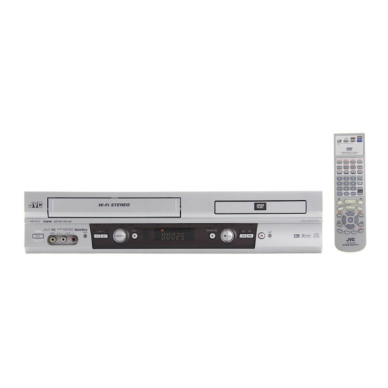
HR-XV2EK
POWER
VCR
DVD
TV
DVD MENU MEMORY
SEARCH
SUBTITLE
ANGLE
REPEAT A-B
ZOOM
TITLE
REPEAT
SHOWVIEW
1
2
3
VIDEO Plus+
4
5
6
7
8
9
TV
TV
0
TV/VCR
TV/VCR PR +
OK
0000
CANCEL
TV/VCR PR
Outputs (DVD)
S-VIDEO OUT
COMPONENT VIDEO OUT
Audio output (digital audio)
Audio output (optical audio)
Audio output (analog audio)
Outputs (VCR)
Audio
Video
Design and specifications are subject to change without notice.
Manufactured under license from Dolby Laboratories. " Dolby" and double-D symbol are trademarks of
Dolby Laboratories. Confidential Unpublished Works. ©1992-1997 Dolby Laboratories, Inc. All rights reserved.
Manufactured under license from Digital Theater Systems, Inc. US Pat. No. 5,451,942 and other world-wide patents issued and
pending. " DTS" and " DTS Digital Out" are trademarks of Digital Theater Systems, Inc. Copyright 1996 Digital Theater Systems, Inc.
All rights reserved.
COPYRIGHT © 2003 VICTOR COMPANY OF JAPAN, LTD
(Y) 1.0 Vp-p 75 ohms, negative sync., Mini Din 4-pin x 1
(C) 0.3 Vp-p 75 ohms
(Y) 1.0 V (p-p), 75 Ω, negative sync, RCA jack x 1
(Pb)/(Pr) 0.7 V (p-p), 75 Ω, RCA jack x 2
0.5 V (p-p), 75 Ω, RCA jack x 1
5 V (p-p), 75 Ω, Optical connector x 1
2.0 Vrms (1 kHz, 0 dB), 330 Ω, RCA jack (L, R) x 2/SCART(TO TV)
-6.0dBm, less than 1 kohms (SCART)
1.0Vp-p, 75 ohms, unbalanced (SCART)
PAL
HR-XV2EK D2VP11
No.82985
2003/06
Advertisement
Chapters
Table of Contents

Related Manuals for JVC HR-XV2EK


Summary of Contents for JVC HR-XV2EK
- Page 1 More than 100 dB (DVD) More than 95 dB (CD) Inputs (VCR) Audio -6.0dBm, more than 10 kohms (SCART) -6.0dBm, more than 47 kohms (RCA) Video 1.0 Vp-p, 75 ohms, unbalanced (SCART/RCA) HR-XV2EK D2VP11 No.82985 COPYRIGHT © 2003 VICTOR COMPANY OF JAPAN, LTD 2003/06...
- Page 2 CONTENTS SECTION 1 ..SUMMARY SECTION 3 ..ELECTRICAL SECTION 4 ..MECHANISM OF VCR PART SECTION 5 ..MECHANISM OF DVD PART SECTION 6 ..REPLACEMENT PARTS LIST...
- Page 3 SECTION 1 SUMMARY CONTENTS Safety Precautions SPECIFICATIONS ....................1-5...
-
Page 4: Safety Precautions
Safety Precautions 1. This design of this product contains special hardware and many circuits and components specially for safety purposes. For continued protection, no changes should be made to the original design unless authorised in writing by the manufacturer. Replacement parts must be identical to those used in the original circuits. - Page 5 SPECIFICATIONS DVD PART Power supply AC 110~240V, 50/60 Hz(HR-XV2ER) AC 200~240V, 50/60 Hz(HR-XV2EX/HR-XV2EY/ HR-XV2EL/HR-XV11EX/ HR-XV2EK/HR-XV2EF/HR-XV2EZ) Power consumtion Mass 5.4kg External dimensions 430 x 97.5 x 293 (W x H x D) Signal system PAL 625/50 Laser Semiconductor laser, wavelength 650nm...
-
Page 6: Table Of Contents
SECTION 3 ELECTRICAL CONTENTS OVERALL BLOCK DIAGRAM DVD PART ......3-2 VCR PART ELECTRICAL TROUBLESHOOTING GUIDE & WAVEFORMS ........3-52 ELECTRICAL ADJUSTMENT 1. System Clock X501 (27Mhz) .......3-52 PROCEDURES ............3-3 2. Initializing between MPEG and SDRAM ....3-52 3. Initializing between MPEG and Flash ....3-53 ELECTRICAL TROUBLESHOOTING 4. - Page 7 VCR PART ELECTRICAL ADJUSTMENT PROCEDURES 1. Servo Adjustment 1) PG Adjustment •Test Equipment b) NTSC MODEL : NTSC SP TEST TAPE a) OSCILLOSCOPE C) PAL MODEL : PAL SP TEST TAPE • Adjustment And Specification MODE MEASUREMENT POINT ADJUSTMENT POINT SPECIFICATION V.Out 6.5 ±...
- Page 8 ELECTRICAL TROUBLESHOOTING GUIDE 1. Power(SMPS) CIRCUIT (1) No 5.3VA (SYS/TUNER) (2) No 12VA (TO CAP, DRUM MOTOR) NO 5.3VA. NO 12VA. Replace the F101. Is the Vcc(13V) supplied Check or Replace Is the F101 normal? (Use the same Fuse) to (+) terminal in D115? the D110.
- Page 9 (4) No 5V (TO DVD) (5) No 33V (TUNER) NO 5V. No 33V. Is 5.3VA put into Check the Power 5.3VA Line Check. Is Q162 Base “H”? the Q160 Emitter? Control. Is the Q162 Base Check the Power Check or Replace “H”? Control.
- Page 10 (7) No 8V(TO DVD) (8) No 3.3V(TO DVD) NO 8V. NO 3.3V. Check or Replace Check or Replace Is Vcc(13V) supplied to Is Vcc(4V) supplied (+) terminal in D114? to IC152 Pin1? the D110. the D111. Check or Replace Check the Power Is Vcc(12V) supplied Is the Q162 Base to IC151 Pin1?
- Page 11 2. SYSTEM/KEY CIRCUIT (1) AUTO STOP Auto Stop Does the SW25 waveform Check the Drum Motor appear at the IC501 signal. Pin105? Do T/UP Reel Pulses Do the T-UP Reel Pulses Does 5.2V appear at the appear at the Q514 appear at the IC501 Pin49? RS501? Base terminal ?
- Page 12 3. SERVO CIRCUIT (1) Unstable Video in PB MODE Unstable Video in PB Mode. Does the Noise level of the screen change periodically? Do the CTL pulses appear Is adjusting the height of at the IC501 Pin8? the CTL Head accurate? Does the CFG waveform Readjust the height of the appear at the IC501...
- Page 13 2. SERVO CIRCUIT (3) When the Capstan Motor doesn’t run, When the Capstan Motor doesn’t run, Refer to “SMPS(CAPSTAN/12Volt) Does 12VA appear at the PMC01? Trouble Shooting”. Does 2.8V appear at the PMC01? Check the PMC01 and the Capstan Does the PWM signal appear at the Motor Ass’y.
- Page 14 (4) KEY doesn’t working KEY doesn’t working. Is 5V applied to the IC501 Refer to “SMPS 5.3VA Pin36? Trouble Shooting”. Does LED or FLD change Replace the defective when a function button is switches. pressed? 3-10...
- Page 15 4. Y/C CIRCUIT (1) No Video in EE Mode, No Video in EE Mode Does the Video signal Check the 24Pin of Tuner. appear at the IC301 Pin15? Is 5V applied to the IC301 Check the 5.2VT, 5.3VA Pins4, 22, 47, 60, 84? Line.
- Page 16 3. Y/C CIRCUIT (2) When the Y(Luminance) signal doesn’t appear on the screen in PB Mode, Is 5.2VT, 5.3VA applied to the Check the line of the 5.2VT, 5.3VA Line. (Power Circuit) IC301 Pins22, 47, 60, 84? Is the I C Bus siganl applied Refer to ‘SYSTEM I C BUS...
- Page 17 3. Y/C CIRCUIT (3) When the C(Color) signal doesn’t appear on the screen in PB Mode, Is 5.2VT/5.3VA applied to the Check the line of the 5.2VT/ 5.3VA Line. (Power Circuit) IC301 Pins22, 47, 60, 84? Does the Color signal Does the X301(4.43MHZ) appear at the IC301 Replace the X301.
- Page 18 3. Y/C CIRCUIT (4) When the Video signal doesn’t appear on the screen in REC Mode, Is the EE signal normal? Check EE Mode. Is 5.2VT/5.3VA applied to the Check the line of the 5.2VT/ IC301 Pins4, 22, 47, 60, 84 5.3VA Line.(Power Circuit) Does PB Mdoe operate Check PB Mode.
- Page 19 5. Hi-Fi CIRCUIT (A) No Sound(EE Mode) No Sound. Check the TU Audio of IC801 Check the IC751 Pins30, 31. Pins2, 3. Check the DVD Audio of IC801 Check the DVD MODULE. (PMD02 Pins13, 15). Pins4, 5. Check the AV1 Audio of IC801 Check the Scart1 Jack.
- Page 20 3. Y/C CIRCUIT (B) Hi-Fi Playback PB mode No Sound. Check the Vcc of IC801 Check Power 5.2V, 12VT. (Pins34, 40) Check the Hi-Fi Selection switch. Check IC501 Pin106 (IC801 Pin41) and the Tape quality. (A.H/SW) Is the RF Envelope at IC801 Pin44 over 2Vp-p? Check the parts of µ-COM Check IC801 Pin42(Data),...
- Page 21 Hi-Fi REC. It can’t be recorded Hi-Fi Audio signal. Check Vcc of IC801.(Pins34, 40) Check Power 5V, 12VT. Check ports of µ-COM. Check IC801 Pin42(Data), Pin43(CLOCK). (IC501 pins 59, 60) Check Audio input signal of IC801 Do Audio signals appear at IC801 Pins2, 3(TU.A.), 4, 5(DVD.A.), Pins16, 17? 6, 7(AVI.A.), 8, 9(AV2.A.), 10, 11(AV3.A.).
- Page 22 6. Tuner/IF CIRCUIT (A) No Picture on the TV screen No picture on the TV screen Does the Video signal at Is +33V applied to TU701 Check 33V line. the TU701 Pin24. Pin16? Is +5V applied to TU701 Check 5V line. Pin13? Does the Clock signal Check the lIC Clock Signal...
- Page 23 (B) No Sound No Sound. Check the Vcc of IC751 Pins1, 11, 19, Check 5.2V Line. 22, 33. Check the Tuner SiF signal at IC751 Check the Tuner SIF of TU701 Pin22. Pin2. Check the oscillator of IC751 Pins5, 6. Replace X751 Check the IIC Clock and Data at IC751 Check the Audio of IC751 Pins30, 31.
-
Page 24: Dvd Part
DVD PART ELECTRICAL TROUBLESHOOTING GUIDE 1. µ-COM Circuit A. No Power POWER ON Does Hello appear at FLD? Is PDV02 Does no DISC appear? connected normally? Reconnect it. Does Logo appear Check power. on the screen? (Refer to power) If power is normal Is PDV02 Pins8, 9, 10, 11 normal? - Page 25 B. Audio abnormal C. Video abnormal AUDIO ABNORMAL VIDEO ABNORMAL Check Audio jack. Check Video jack. YES (If OK) YES (If OK) Check MPEG_CLK Signal Refer to Video part. (IC501 Pin22) of MPEG part. YES (If OK) YES (If OK) Refer to Audio part.
- Page 26 E. Picture abnormal PICTURE ABNORMAL Check the disc. Refer to Servo part If OK Check MPEG_CLK Signal (IC501 Pin22) of MPEG part YES (If OK) Check DSP YES (If OK) Check MPEG YES (If OK) Replace Main B/D F. Disc Error DISC ERROR Check Disc YES (If OK)
-
Page 27: Mpeg Circuit
2. MPEG Circuit Power is on Does Logo appear Check power & clock. on the screen? Does the Check CD/DVD DSP output moving picture of the DVD Disc Is MPEG data signal normal? play on the screen signal. normally? Check MPEG Decoder input signal. - Page 28 3. RF/Servo Circuit CHECK POINT(General) Does signal goes "High" to IC201 Pin186 when the power is on? Does signal pulse Check "2.µ-COM Part". input to IC201 Pins53, 54 when the power is on? Does Does Replace X201 or IC206 33.8688MHz clock input to 33.8688MHz clock input (33MHz clock defect) IC201 Pin138?
- Page 29 No disc Power on. Check loading Part. Push Pick-up to inner track to Does tray open or close? the end by hand. Does DECK assembly is defective. PMD03 Pin10 change (Limit sw) high to low? Pressing the open/close key check µ-COM Part. repeatedly, check the voltage of IC2M1 Pins14, 15 change 0V to 5V...
- Page 30 DISC IN OPEN/CLOSE Fig.3. FOCUS ERROR waveform Check Check IC2A1 Pins47,50,51,52 the focus error moving the FOCUS ON? lens up and down. in DVD Mode (IC2A1 Pin39) IC201 no output : Pick-up is defective. Does the TTL level change at IC201 Replace IC201.
- Page 31 CHECK A Fig.5. RF waveform Check RF Eye-Pattern. Check IC2A1 Pin3. No signal: Pick-up is defective RF : 1.5-1.6V(TP2A0) Does the sawtooth waveform emit Is the eye-pattern vivid? Does the 1.6V emit? Replace IC2A1. at IC2A1 Pin36? Replace IC201. Check IC201 Pin84. No signal at IC201 : IC201 is defective •...
- Page 32 SECTION 4 MECHANISM OF VCR PART CONTENTS DECK MECHANISM PARTS DECK MECHANISM ADJUSTMENT LOCATIONS • Tools and Fixtures for Service ....4-12 1. Mechanism Alignment Position Check..4-13 • Top View............4-1 2. Preparation for Adjustment......4-14 • Bottom View ..........4-1 3. Checking Torque ........4-14 4.
-
Page 33: Deck Mechanism Parts Locations
DECK MECHANISM PARTS LOCATIONS • Top View Procedure Fig- Part Fixing Type Starting 1 Drum Assembly 3 Screw 2 Plate Top 2 Hook 3 Holder Assembly CST Chassis Hole 4 Opener Door Chassis Hole 5 Bracket Assembly 3 Hook L/D Motor 2,3,4 6 Gear Assembly Rack F/L 1 Hook, Chassis Hole A-2... -
Page 34: Deck Mechanism Disassembly
DECK MECHANISM DISASSEMBLY Stator (S2) (S2) (S3) Drum Motor (S3) Rotor Drum Sub Assembly (Fig. A-1-1) Drum FPC Carbon Brush (S1) (S1) (S1) Holder FPC Fig. A-1 (Fig. B-1) 1. Drum Assembly (Fig. A-1-1) 1) Unplug the Drum FPC Connector. 2) Remove three Screws(S1) on bottom side and separate the Drum assembly. - Page 35 DECK MECHANISM DISASSEMBLY (Fig. A-2-1) Plate Top (B') (Fig. A-2-2) Holder Assembly CST (Fig. A-2-6) Arm Assembly F/L (C1) (Fig. A-2-7) Lever Assembly S/W (H8) Bracket Assembly L/D Motor Spring Lever S/W (Fig. A-2-4) (C') (E') Opener Door (Fig. A-2-3) (H6) Chassis Gear Assembly Rack F/L...
-
Page 36: Plate Top
DECK MECHANISM DISASSEMBLY 2. Plate Top (Fig. A-2-1) 2) Unhook three Hooks(H3, H4, H5) on bottom side of the Chassis, lift up the Bracket Assembly L/M and disassem- 1) Pull the (B) portion of the Plate Top back in direction of ble the Bracket Assembly L/D Motor. -
Page 37: Arm Assembly Cleaner
DECK MECHANISM DISASSEMBLY Arm Assembly Cleaner (Fig. A-3-1) (S4) Base Assembly A/C Head (Fig. A-3-3) Head F/E (Fig. A-3-2) Chassis Fig. A-3 9. Arm Assembly Cleaner (Fig. A-3-1) 11. Base Assembly A/C Head (Fig. A-3-3) 1) Breakaway the (A) portion as Fig. A-3-1 from the 1) Remove the Screw(S4) and lift the Base Assembly A/C embossing of the Chassis, turn the Arm assembly Head up. -
Page 38: Brake Assembly T
DECK MECHANISM DISASSEMBLY Arm Assembly Tension (Fig. A-4-3) (H11) Spring TB Brake Assembly T (Fig. A-4-1) Spring Tension Reel S Reel T (Fig. A-4-4) (Fig. A-4-4) Spring RS Brake Assembly RS (Fig. A-4-2) (H12) (H9) (H10) Base Tension Chassis Fig. A-4 12. -
Page 39: Base Assembly P4
DECK MECHANISM DISASSEMBLY Opener Lid (Fig. A-5-2) Assembly Pinch (Fig. A-5-3) Base Assembly P4 Lever T/up (H13) (Fig. A-5-1) (Fig. A-5-4) (H13) Arm T/up (Fig. A-5-5) Chassis Fig. A-5 16. Base Assembly P4 (Fig. A-5-1) NOTE 1) Breakaway the (A) portion of the Base Assembly P4 from When reassembling, confirm the (C) portion of the Arm the embossing of the Chassis. -
Page 40: Belt Capstan/Motor Capstan
DECK MECHANISM DISASSEMBLY Belt Capstan (Fig. A-6-1) Motor Capstan (Fig. A-6-2) Washer(W1) Clutch Assembly D35 (Fig. A-6-4) (L1) (L1) Brake Assembly Capstan (Fig. A-6-5) Lever F/R (Fig. A-6-3) (L2) Chassis (S5) Fig. A-6 20. Belt Capstan (Fig. A-6-1)/ 22. Clutch Assembly D35 (Fig. A-6-4) Motor Capstan (Fig. -
Page 41: Gear Drive/Gear Cam
DECK MECHANISM DISASSEMBLY (H14) Gear Cam Hole(B) Gear Cam (Fig. A-7-2) Gear Drive Hole(A) Gear Sector Washer (W2) (Fig. A-7-3) Plate Slider Gear Drive (Fig. A-7-4) (Fig. A-7-1) Lever Tension (Fig. A-7-5) Lever spring (L3) (Fig. A-7-6) Gear Drive Hole(C) Base Loading (H15) (H16) -
Page 42: Gear Assembly P2
DECK MECHANISM DISASSEMBLY Gear Assembly P2 Hole Gear Assembly P3 Hole Gear Assembly P3 (Fig. A-8-2) Gear Sector Hole(A) Lever Spring Boss Gear Assembly P2 Plate Slider Hole(B) (Fig. A-8-1) Chassis Base Assembly P3 (Fig. A-8-4) Base Assembly P2 (Fig. A-8-3) Fig. -
Page 43: Base Loading
DECK MECHANISM DISASSEMBLY (S7) Base Tension Base Loading (Fig. A-9-2) Arm Assembly Idler (Fig. A-9-1) (Fig. A-9-3) Chassis Fig. A-9 31. Base Loading (Fig. A-9-1) 33. Arm Assembly Idler (Fig. A-9-3) 1) Remove the Screw(S7). 1) Make narrower the two parts, (B) and (C), as Fig. A-9-3. 2) Lift the Base Loading up. -
Page 44: Deck Mechanism Adjustment
DECK MECHANISM ADJUSTMENT • Tools and Fixfures for Service 1. Cassette Torque Meter 2. Alignment Tape 3. Torque Gauge PUJ42881 NTSC: MHP PUJ48075-2 PAL: MHPE 5. Post Height Adjusting Driver (Roller driver) PTU94002 4-12... -
Page 45: Mechanism Alignment Position Check
DECK MECHANISM ADJUSTMENT 1. Mechanism Alignment Position Check Purpose:To determine if the Mechanism is in the correct position, when a Tape is ejected. Test Conditions (Mechanism Test Equipment/ Fixture Check Point Condition) • Mechanism and Mode Switch Position • Blank tape •... -
Page 46: Preparation For Adjustment
DECK MECHANISM ADJUSTMENT 2. Preparation for Adjustment (To set the cassette without tape. Cover the holes of the End Sensors at the both sides of Deck Mechanism of the loading state the Chassis to prevent a light leak. without inserting a cassette tape). Then the Deck Mechanism drives to the Stop Mode. -
Page 47: Guide Roller Height Adjustment
DECK MECHANISM ADJUSTMENT 4.Guide Roller Height Adjustment Purpose: To regulate the height of the tape so that the bottom of the tape runs along the tape guide line on the Lower Drum. 4-1. Preliminary Adjustment Test Equipment/ Fixture Test Conditions (Mechanism Condition) Adjustment Point •... -
Page 48: Audio/Control (A/C) Head Adjustment
DECK MECHANISM ADJUSTMENT 5. Audio/Control (A/C) Head Adjustment Purpose: To insure that the tape passes accurately over the Audio and Control Tracks in exact alignment of the both Record and Playback Modes. 5-1. Preliminary Adjustment (Height and Tilt Adjustment) Perform the Preliminary Adjustment, when there is no Audio Output Signal with the Alignment Tape. Test Equipment/ Fixture Test Conditions (Mechanism Condition) Adjustment Point... -
Page 49: Precise Adjustment(Azimuth Adjustment)
DECK MECHANISM ADJUSTMENT 5-2. Confirm that the tape passes smoothly (2) If folding or curling is observed at the top of it then slowly turn the Tilt Adjustment Screw(C) in the between the Take-up Guide and Pinch counterclockwise direction. Roller(using a mirror or the naked eye). 1) After completing Step 5-1.(Preliminary Adjustment), check NOTE: that the tape passes around the Take-up Guide and Pinch... -
Page 50: Adjustment After Replacing Drum Assembly (Video Heads)
DECK MECHANISM ADJUSTMENT 7. Adjustment after Replacing Drum Assembly (Video Heads) Purpose: To correct for shift in the Roller Guide and X value after replacing the Drum. Test Conditions Test Equipment/ Fixture Connection Point Adjustment Points (Mechanism Condition) • CH-1: PB RF Envelope •... -
Page 51: Maintenance/Inspection Procedure
MAINTENANCE/INSPECTION PROCEDURE 1. Check before starting repairs The following faults can be remedied by cleaning and oil- ing. Check the needed lubrication and the conditions of cleanliness in the unit. Check with the customer to find out how often the unit is used, and then determine that the unit is ready for inspec- tion and maintenance. -
Page 52: Required Maintenance
MAINTENANCE/INSPECTION PROCEDURE 2. Required Maintenance 4. Supplies Required for Inspection and Maintence The recording density of a VCR(VCP) is much higher than that of an audio tape recorder. VCR(VCP) components must (1) Grease : Kanto G-311G (Blue) or equivalent be very precise, at tolerances of 1/1000mm, to ensure com- (2) Isopropyl Alcohol or equivalent patibility with the other VCRs. -
Page 53: Greasing
MAINTENANCE/INSPECTION PROCEDURE 5-2) Greasing (2) Periodic greasing Grease specified locations every 5,000 hours. (1) Greasing guidelines 1) Loading Path Inside & Top side 6) Plate Slider Guide Sections Apply grease, with a cleaning patch. Do not use exces- 2) Base Assembly P2,P3 stopper 7) Plate Slider Guide Sections sive grease. - Page 54 MAINTENANCE/INSPECTION PROCEDURE Lever, F/R, Base, Tension GEAR AY, P2 & P3 Boss Lever, F/R Base, Tension Clutch (G-754. Yellow) Arm Tension Guide Hole 4-22...
-
Page 55: Mechanism Troubleshooting Guide
MECHANISM TROUBLESHOOTING GUIDE 1.Deck Mechanism Auto REW doesn't work. Is the output of END sensor of supply side "H"? “H”: more than 3.5V “L”: less than 0.7V~1V Is the Vcc. voltage of End Check the syscon power. sensor 5V? Replace the End sensor. Is the voltage across IR LED Replace the IR LED. - Page 56 MECHANISM TROUBLESHOOTING GUIDE AUTO STOP. (PLAY/CUE/REV) Check alignment positions (page 4-13). In Play/Cue/Rev, Is the Pinch Roller in contact with the Is the output of DFG, DPG OK? Replace the Drum Motor. Capstan Shaft? Are there T/up and Supply Reel Check the Servo, Syscon.
- Page 57 MECHANISM TROUBLESHOOTING GUIDE In PB mode Tape Presence not sensed. Is the Pinch Roller attached Check Alignment positions to the Capstan Motor Shaft? (page 4-13). Does the T/Up Reel turn? Is the Belt ok? Replace the Belt. Check the Clutch and Idler Does the Capstan Motor turn? Assembly.
-
Page 58: Front Loading Mechanism
MECHANISM TROUBLESHOOTING GUIDE 2. Front Loading Mechanism Cassette cannot be inserted. Does the Lever Assembly Is the Lever Assembly Switch Replace or add the Lever Switch work? Spring damaged or omitted? Assembly Switch Spring. Does the CST IN Switch work Replace the CST IN Switch. - Page 59 MECHANISM TROUBLESHOOTING GUIDE Cassette does not load. Does the cassette insert? Does the Opener Lid work? Does the Gear Assembly Rack F/L Replace the Opener Lid. work? Replace the Gear Rack F/L. Does the Opener Door work? Check the opener Door assembled Does the Arm Assembly F/L work? correctly.
-
Page 60: Exploded Views
EXPLODED VIEWS 1. Front Loading Mechanism Section 4-28... -
Page 61: Moving Mechanism Section (1)
EXPLODED VIEWS 2. Moving Mechanism Section(1) OPTIONAL PART 4-29... -
Page 62: Moving Mechanism Section (2)
EXPLODED VIEWS 3. Moving Mechanism Section(2) OPTIONAL PART 4-30... - Page 63 SECTION 5 MECHANISM OF DVD PART CONTENTS 5. Frame Assembly Up/Down ....5-4 DECK MECHANISM PARTS 6. Belt Loading........5-4 LOCATIONS 7. Gear Pulley ........5-4 8. Gear Loading ........5-4 • Top View..........5-1 9. Guide Up/Down.........5-4 • Top View(without Tray Disc) ....5-1 • Bottom View ...........5-1 10.
- Page 64 DECK MECHANISM PARTS LOCATION • Top View (With Tray) Procedure Disass Fig- Parts Fixing Type embly Starting No. Holder 2 Screws, Clamp 2 Locking Tabs Clamp Assembly Disc 1, 2 Plate Clamp 1, 2, 3 Magnet Clamp 1, 2, 3, 4 Clamp Upper Tray Disc 1, 6...
- Page 65 DECK MECHANISM DISASSEMBLY HOLDER CLAMP PLATE CLAMP CLAMP ASSEMBLY DISC MAGNET CLAMP TRAY DISC CLAMP UPPER (S1) (Fig. A) HOLDER CLAMP BASE MAIN EMERGENCY EJECT HOLE (L1) BASE MAIN LEVER HOLDER CLAMP (L1) BASE MAIN BOTTOM SIDE VIEW Fig. 5-1 ig.
- Page 66 DECK MECHANISM DISASSEMBLY (L2) GEAR MIDDLE (S2) (BLACK) (S3) GEAR ASSEMBLY RACK GEAR ASSEMBLY FEED (S2) (BLACK) (S2) RUBBER REAR (GREEN) PICK UP ASSEMBLY GENERAL BASE PU(OUTSERT) (C1) (S2) (GREEN) PICK UP ASSEMBLY GENERAL GEAR ASSEMBLY FEED MOTOR ASSEMBLY SPINDLE GEAR MIDDLE GAER ASSEMBLY RACK MOTOR ASSEMBLY SPINDLE...
- Page 67 DECK MECHANISM DISASSEMBLY GUIDE UP/DOWN GEAR LOADING (L3) (L6) GEAR PULLEY (L6) (L4) BELT LOADING BASE MAIN PWB ASSEMBLY LOADING (H1) (L6) (S5) (C2) BASE MAIN (S4) FRAME ASSEMBLY UP/DOWN (L5) GUIDE UP/DOWN FIG. (A) FIG. (B) GUIDE UP/DOWN GUIDE UP/DOWN FIG.
- Page 68 EXPLODED VIEWS 1. Deck Mechanism Exploded View 011A...
- Page 69 VICTOR COMPANY OF JAPAN, LIMITED AV & MULTIMEDIA COMPANY. 12,3-chome,Moriya-cho,Kanagawa-ku,Yokohama,Kanagawa-prefecture,221-8528,Japan Printed in Japan 0306 VP...
- Page 70 OVERALL WIRING DIAGRAM...
-
Page 71: Block Diagrams
BLOCK DIAGRAMS 1. POWER(SMPS) BLOCK DIAGRAM R101 SNUBBER BD101 BLOCK FROM µ-COM (D101, R104, HSR SW C105, C106) RECTIFIER & HSR 'H' BLOCK SMOOTHING C103 (Q155, Q153, Q154, ZD104, C156, R161, (D106, C117, R130) R151, R152, R110) RECTIFIER & SMOOTHING TO CAP MOT 12VA DRIVE &... - Page 72 2. Tu/IF, NICAM & A2 BLOCK DIAGRAM 3. VPS BLOCK DIAGRAM 3-22 3-23...
- Page 73 4. Y/C BLOCK DIAGRAM (PB MODE) (REC MODE) 3-24 3-25...
- Page 74 5. Hi-Fi BLOCK DIAGRAM Hi-Fi/ AUDIO INPUT 36 35 BLOCK Tu A.IN 'L' Tu A.IN 'R' A.OUT 'L' DVD A.IN 'L' A.OUT DVD A.IN 'R' IC803 To JACK A.OUT 'R' IC801 EU1 A.IN 'L' EU1 A.IN 'R' EU2 A.IN 'L' EU2 A.IN 'R' AV2 A.IN 'L' AV2 A.IN 'R'...
- Page 75 6. SYSTEM BLOCK DIAGRAM LD(+) LD(-) OTPB LED 'H' IC501 CANAL DET 'H' HD6432197A L/M CONTROL R525, R526 R/C IN(2W) CST SW 2fsc R524, R514, R518, R516, R589, C577, C576, L501, Q504 3-28 3-29...
-
Page 76: Circuit Diagrams
2. Voltages are DC-measured with a digital voltmeter MODIFIED OR ALTERED WITHOUT PERMISSION IMPLEMENTATION OF THE LATEST SAFETY AND during Play mode. FROM THE JVC ELECTRONICS CORPORATION. ALL PERFORMANCE IMPROVEMENT CHANGES INTO COMPONENTS SHOULD BE REPLACED ONLY WITH THE SET IS NOT DELAYED UNTIL THE NEW SERVICE TYPES IDENTICAL TO THOSE IN THE ORIGINAL CIR- LITERATURE IS PRINTED. - Page 77 2. TU/IF, NICAM & A2 CIRCUIT DIAGRAM '03. 4. 7 SR14506A EE MODE(VIDEO) VJW602CP's TU MODE (AUDIO) 3-32 3-33...
- Page 78 3. A/V CIRCUIT DIAGRAM No Color. R333, C357, C358 are defective. Video Noise. No Color. H/SW Level is defective.. L307, C349 are defective. Video output level unstable C332 is defective. VIDEO Distortion WAVEFORM R322, R323, R324, Y. (REC) Y+C (REC) C320 are defective.
- Page 79 4. Hi-Fi CIRCUIT DIAGRAM 44 Pin is defective. IC801 Pins42, 43 aredefective. Hi-Fi Audio is not appear. All Audio is not appear. '03. 4. 7 SR14503A VJW602CP's 3-36 3-37...
- Page 80 5. SCART(JACK) CIRCUIT DIAGRAM '03. 4. 7 SR14505B VJW602CP's 3-38 3-39...
- Page 81 6. SYSTEM CIRCUIT DIAGRAM SW is defective. Key service dead. CLOCK SETTING will not operate. X501 is defective. Reset is defective. Set dead. µ-COM will not operate. IC504 is defective. X502 is defective. RC501 is defective. R/C will not operate. VCR will not operate.
- Page 82 • WAVEFORMS * IC301 Waveform * IC501 Waveform V.HSW DV.SYNC CTL(+) CTL(-) (IC501 Pin 105) (IC501 PIN 109) (IC501 Pin 3) (IC501 Pin4) IC301 Pin 9 IC301 Pin 12 IC301 Pins 33, 36, 37 IC301 Pin 15 1V/10mS 1V/100uS 1V/10mS 1V/10mS 100mV/10msec DIV 100mV/10msec DIV...
- Page 83 • CIRCUIT VOLTAGE CHART MODE MODE MODE MODE MODE MODE MODE PIN NO. PIN NO. PIN NO. PIN NO. PIN NO. PIN NO. PIN NO. I C 2 0 1 0.88 0.52 0.03 1.86 V 0.004 V 4.7 V 4,7 V 5.1 V 5.04 V 0.008 V...
- Page 84 MODE PIN NO. 5.6 V 5.58 V 5.59 V Q301 COLECTOR 0.02 V 0.01~4.8V 0.011 V 5.6 V 5.58 V 5.59 V BASE 0.44 Q7S1 EMITER 0.083 BASE 0.007 V 0.007 V 0.008 V 5.54 V 5.5 V 5.5 V 4.16 V 4.32 V 4.51 V...
- Page 85 PRINTED CIRCUIT DIAGRAMS 1. MAIN P.C.BOARD LOCATION GUIDE 3-48 3-49...
- Page 86 2. SMPS P.C.BOARD LOCATION GUIDE NOTES) Warning NOTES) Parts that are shaded are critical NOTES) With respect to risk of fire or NOTES) electricial shock. 3-50 3-51...
-
Page 87: Overall Block Diagram
BLOCK DIAGRAMS 1. DVD OVERALL BLOCK DIAGRAM , PAL_SW , AUTO_SW , MIC_ON DAC_RST /FLASH_CS , /RD PWEO PSENB MIRR,TZC,PE,TE FE,DFECT_IN XLAT , E_STI , E_ENB , E_DR CPLD SPINDLE FOCUS,TRACKI NG,SLED LOADING DECK M ECHANI SM 3-60... -
Page 88: Block Diagrams
2. RF/CD DSP/DVD DSP/DVD SERVO BLOCK DIAGRAM 3-61... - Page 89 3. AUDIO BLOCK DIAGRAM 3-62...
-
Page 90: Mpeg Block Diagram
4. MPEG BLOCK DIAGRAM AD[ 04 : 21 ] 3-63... -
Page 91: Circuit Diagrams
CIRCUIT DIAGRAMS 1. DVD DSP CIRCUIT DIAGRAM TO/FROM MPEG DSP II '02. 12. 04 R17147A TRACKING LOOP SLED LOOP COMBI NS WAVEFORM FOCUS LOOP SPINDLE LOOP 3-64 3-65... - Page 92 2. DRIVE & RF CIRCUIT DIAGRAM TO/FROM MEMORY Q2A5, Q2A6 TO/FROM DSP TO/FROM DSP TO/FROM MEMORY TO/FROM MPEG TO/FROM MEMORY TO/FROM DSP TO/FROM DSP '02. 12. 04 R17145A COMBI NS TRACKING LOOP SLED LOOP WAVEFORM FOCUS LOOP SPINDLE LOOP 3-66 3-67...
- Page 93 3. MEMORY CIRCUIT DIAGRAM Digitron all not display system not working Digitron all not display system not workry DRIVE & RF Digitron all not display system not working Tray not open/close Digitron all not display '02. 12. 04 R17148A system not working Tray not open/close COMBI NS 3-68...
- Page 94 4. INTERFACE CIRCUIT DIAGRAM (TO/FROM VCR POWER) PDV01-PPD01 (TO/FROM VCR SYSTEM) PDV02-PMD01 TO/FROM MPEG TO/FROM JACK TO/FROM MPEG (TO/FROM VCR JACK) PDV03-PMD02 TO/FROM MEMORY '02. 12. 04 R17150A COMBI NS 3-70 3-71...
- Page 95 5. µ-COM/EXPANDER CIRCUIT DIAGRAM HB-1S1608 MM74HCT244 '02. 12. 04 R17146A Optical/Coaxial out Y/Pb/Pr(Componet) WAVEFORM COMBI NS Y/C(S-VHS) CVBS 3-72 3-73...
- Page 96 6. JACK CIRCUIT DIAGRAM DAP202K '02. 12. 04 R17149A COMBI NS 3-74 3-75...
- Page 97 • WAVEFORMS Stop : 2.50MS/s 4 Acqs Glitch Ch1 M20.0µs 2 Apr 1999 500mV 14:47:27 IC2A1 IC2A1 Pin 36 IC2A1 Pin 36 IC501 Pin 118, Composite IC501 Pin 112, Chrominance IC501 Pin 114, Luminance TP2A0 Tracking Error VBR TRACKING Error (Super video out Mode) (Super video out Mode) Stop :...
-
Page 98: Circuit Voltage Chart
• CIRCUIT VOLTAGE CHART MODE MODE MODE MODE MODE MODE MODE MODE MODE MODE STOP PLAY PLAY PLAY PLAY PLAY PLAY PLAY PLAY PLAY PLAY PIN NO. PIN NO. PIN NO. PIN NO. PIN NO. PIN NO. PIN NO. PIN NO. PIN NO. - Page 99 MODE MODE MODE MODE MODE MODE MODE MODE MODE MODE PLAY PLAY PLAY PLAY PLAY PLAY PLAY PLAY STOP PLAY STOP PLAY PIN NO. PIN NO. PIN NO. PIN NO. PIN NO. PIN NO. PIN NO. PIN NO. PIN NO. PIN NO.
- Page 100 MODE MODE PLAY STOP PLAY PIN NO. PIN NO. CAPACITOR Q2A1 C3F3 3.25 5.09 5.05 C293 3.25 5.09 5.24 C262 3.25 0.00 0.00 Q2A2 C281 1.60 C279 2.14 5.07 0.00 C285 2.07 5.07 0.00 C297 3.25 0.00 1.82 Q2A5 C280 2.71 C278 2.13...
-
Page 101: Printed Circuit Diagrams
PRINTED CIRCUIT DIAGRAMS 1. MAIN P.C.BOARD (TOP VIEW) LOCATION GUIDE 3-84 3-85... -
Page 102: Main P.c.board (Bottom View)
2. MAIN P.C.BOARD (BOTTOM VIEW) LOCATION GUIDE 3-86 3-87 E. & O. E. No. 82984 HR-XV2EX, HR-XV2EY,HR-XV2EL, HR-XV11EX (VP)D2VP11 No. 82985 HR-XV2EK... -
Page 103: Specifications
Replace only with specified part numbers. BEWARE OF BOGUS PARTS Parts that do not meet specifications may cause trouble in regard to safety and performance. We recom- mend that genuine JVC parts be used. EXPLODED VIEW 6.1.1 PACKING AND ACCESSORY ASSEMBLY <M1>... - Page 104 6.1.2 FINAL ASSEMBLY <M2> OPTIONAL PARTS A46A...
- Page 105 6.1.3 MECHANISM ASSEMBLY(VCR) <M4> 002A OPTIONAL PART 100A 054A 100B 052A...
- Page 106 6.1.4 MECHANISM ASSEMBLY(DVD) <MN> 011A...
- Page 107 AAM UM-3 SEOTONG 1-5 V - LOL 1 LG-4970R-0122A SPRING COIL D35 LG-6851R-0012B CABLE ASSEMBLY RF-CABLE DOUBLE SHIELD PAL LGE LG-4261R-0020A ARM ASSY LG-6711R2P040A REMOTE CONTROLLER ASSEMBLY JVC COMBI VJW602CP JVC LG-4510R-0047A LEVER SPRING LG-3300R-M116A PLATE SLIDER ****************************** LG-4510R-0041A LEVER...
- Page 108 NSP:Not Service Parts # REF No. PART No. PART NAME, DESCRIPTION SPECIFICATION # REF No. PART No. PART NAME, DESCRIPTION SPECIFICATION ---- ------- ----------------------- -------------------------------------- -------------------------------------- ------------------------ ---- ------- ----------------------- -------------------------------------- -------------------------------------- ------------------------ ****************************** R130 QRD161J-104Y RESISTOR,FIXED CARBON FILM 100K OHM 1/6 W 5% TA26 R131 QRE121J-224Y RESISTOR,FIXED CARBON FILM 220K OHM 1/6 W 5% TA26...
- Page 109 NSP:Not Service Parts # REF No. PART No. PART NAME, DESCRIPTION SPECIFICATION # REF No. PART No. PART NAME, DESCRIPTION SPECIFICATION ---- ------- ----------------------- -------------------------------------- -------------------------------------- ------------------------ ---- ------- ----------------------- -------------------------------------- -------------------------------------- ------------------------ C356 LG-0CH1333K562 CAPACITOR,CHIP[CERAMIC M/L HD 0.033UF 50V K X7R(X) 1508 R/TP C710 LG-0CE4754K638 CAPACITOR,FIXED ELECTROLYTIC 4.7UF SRA,SS 50V 20% FM5 TP 5 C357 LG-0CH1223K942...
- Page 110 NSP:Not Service Parts # REF No. PART No. PART NAME, DESCRIPTION SPECIFICATION # REF No. PART No. PART NAME, DESCRIPTION SPECIFICATION ---- ------- ----------------------- -------------------------------------- -------------------------------------- ------------------------ ---- ------- ----------------------- -------------------------------------- -------------------------------------- ------------------------ D902 1SS133-T2 DIODE,SWITCHING 1SS133 DETECT,SW TP Q503 LG-0TR127309AA TRANSISTOR KTA1273-TP-Y (KTA966A)KEC ES50 LG-4931R-0050C...
- Page 111 NSP:Not Service Parts # REF No. PART No. PART NAME, DESCRIPTION SPECIFICATION # REF No. PART No. PART NAME, DESCRIPTION SPECIFICATION ---- ------- ----------------------- -------------------------------------- -------------------------------------- ------------------------ ---- ------- ----------------------- -------------------------------------- -------------------------------------- ------------------------ R553 NRSA6AD-221W RESISTOR,METAL GLAZED(CHIP) 220 OHM 1 / 10 W 2012 5.00% D R803 NRSA6AD-272W RESISTOR,METAL GLAZED(CHIP) 2.7K OHM 1 / 16 W 1608 5.00% D...
- Page 112 NSP:Not Service Parts # REF No. PART No. PART NAME, DESCRIPTION SPECIFICATION # REF No. PART No. PART NAME, DESCRIPTION SPECIFICATION ---- ------- ----------------------- -------------------------------------- -------------------------------------- ------------------------ ---- ------- ----------------------- -------------------------------------- -------------------------------------- ------------------------ X501 LG-6202R31001F RESONATOR,CRYSTAL HC-49S KEUMSEOK 10-0000MHZ 30P C2A9 LG-0CH1104K942 CAPACITOR,CHIP[CERAMIC M/L HD 0.1UF 50V Z Y5V(F) 1508 R/TP X502 QAX0444-001...
- Page 113 MBM29LV800BA-90PFTN FUJITSU 48 R2B5 NRSA63J-102X RESISTOR,METAL GLAZED(CHIP) 1K OHM 1 / 16 W 1608 5.00% D IC3F1A LG-6957R-412AA PROGRAM VJW602CS (JVC) DVD PROGRAM R2B6 NRSA63J-180X RESISTOR,METAL GLAZED(CHIP) 18 OHM 1 / 16 W 1608 5.00% D IC401 LG-0IPRPCI003B IC,PERIPHERALS CS4391-KZR CIRRUS LOGIC 20 TSS...
- Page 114 4.7K OHM 1 / 16 W 1608 5.00% D R416 NRSA63J-822X RESISTOR,METAL GLAZED(CHIP) 8.2K OHM 1 / 16 W 1608 5.00% D R417 NRSA63J-182X RESISTOR,METAL GLAZED(CHIP) 1.8K OHM 1 / 16 W 1608 5.00% D 6-12 (VP)-D2VP11 E. & O. E. No.82985 HR-XV2EK...
Need help?
Do you have a question about the HR-XV2EK and is the answer not in the manual?
Questions and answers