Table of Contents
Advertisement
Quick Links
QQ
3 7 63 1515 0
SERVICE MANUAL
Ver 1.0 2001.04
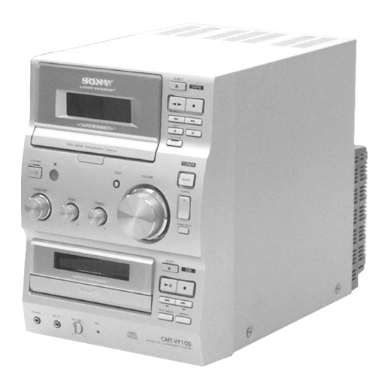
HCD-VP100 is the Amplifier, Video CD
player, Tape Deck and Tuner section in
CMT-VP100.
TE
L 13942296513
www
.
Sony Corporation
9-873-828-11
2001D0500-1
Home Audio Company
C 2001.4
Shinagawa Tec Service Manual Production Group
http://www.xiaoyu163.com
Amplifier section
The following measured at 230 V AC, 60 Hz
DIN power output (rated): 27 + 27 W
(6 ohms at 1 kHz, DIN)
Continuous RMS power output (reference):
32 + 32 W
(6 ohms at 1 kHz, 10%
THD)
The following measured at 220 V AC, 60 Hz
DIN power output (rated): 23 + 23 W
(6 ohms at 1 kHz, DIN)
Continuous RMS power output (reference):
26 + 26 W
(6 ohms at 1 kHz, 10%
THD)
Inputs
AUDIO IN MD (VIDEO) (phono jacks):
Sensitivity 500/250 mV,
impedance 47 kilohms
MIC IN (minijack):
Sensitivity 1 mV,
impedance 10 kilohms
Outputs
OPTICAL DIGITAL OUT (CD):
Optical
VIDEO OUT (phono jack):
max. output level 1 Vp-p,
unbalanced, Sync
negative, load impedance
75 ohms
PHONES (stereo minijack):
Accepts headphones with
an impedance of 8 ohms
or more
x
ao
y
i
http://www.xiaoyu163.com
HCD-VP100
8
Model Name Using Similar Mechanism
CD
Section
CD Mechanism Type
Tape deck
Model Name Using Similar Mechanism
Section
SPECIFICATIONS
Q Q
3
6 7
1 3
VIDEO CD/CD player section
System
Laser
Wavelength
Video color system format
OPTICAL DIGITAL OUT (CD)
(Square optical connector jack, rear panel)
Wavelength
Output Level
Tape player section
Recording system
Frequency response
Wow and flutter
MICRO Hi-Fi COMPONENT SYSTEM
u163
.
2 9
9 4
2 8
1 5
0 5
8
2 9
9 4
Compact disc and digital
audio and video system
Semiconductor laser
(λ = 780 nm)
Emission
duration: continuous
780 - 790 nm
NTSC, PAL
660 nm
–18 dBm
4-track 2-channel stereo
50 - 13,000 Hz (±3 dB),
using a Sony TYPE I
cassette
±0.15% W. Peak (IEC)
0.1% W. RMS (NAB)
±0.2% W. Peak (DIN)
– Continued on next page –
m
co
9 9
E Model
NEW
CDM55F-K6BD42A
HCD-CP100
2 8
9 9
Advertisement
Table of Contents

Related Manuals for Sony HCD-VP100


Summary of Contents for Sony HCD-VP100
- Page 1 HCD-VP100 3 7 63 1515 0 SERVICE MANUAL E Model Ver 1.0 2001.04 HCD-VP100 is the Amplifier, Video CD player, Tape Deck and Tuner section in CMT-VP100. Model Name Using Similar Mechanism Section CD Mechanism Type CDM55F-K6BD42A Tape deck...
-
Page 2: Table Of Contents
HCD-VP100 3 7 63 1515 0 Tuner section TABLE OF CONTENTS FM stereo, FM/AM superheterodyne tuner GENERAL FM tuner section Tuning range 87.5 - 108.0 MHz Location of Controls ............4 (50-kHz step) Setting the Time .............. 5 Antenna... - Page 3 LINE WITH MARK 0 ON THE SCHEMATIC DIAGRAMS AND IN THE PARTS LIST ARE CRITICAL TO SAFE OPERATION. REPLACE THESE COMPONENTS WITH SONY PARTS WHOSE PART NUMBERS APPEAR AS SHOWN IN THIS MANUAL OR IN SUPPLEMENTS PUB- LISHED BY SONY.
-
Page 4: Location Of Controls
HCD-VP100 SECTION 1 This section is extracted from instruction manual. 3 7 63 1515 0 GENERAL • LOCATION OF CONTROLS – Front View – > BASS 3 (20) PBC indicator wd (10, 28) TREBLE 4 (20) L 13942296513 CD EJECT Z qj (9~11) -
Page 5: Setting The Time
HCD-VP100 3 7 63 1515 0 – Rear View – Setting the time Turn on the system. Press CLOCK/TIMER SET on the remote. If you are setting the clock for the first time, go to step 5. Press +/– on the remote repeatedly until “SET CLOCK”... - Page 6 HCD-VP100 3 7 63 1515 0 Remote Control CD ql (9, 11) CLOCK/TIMER SELECT 4 1 2 3 (19, 22) CLOCK/TIMER SET 5 (8, 18, DIR MODE wh (16~18) DISPLAY wj (12) ENTER 8 (8, 14, 18, 21) FUNCTION qj (9, 11, 12, 14, 16,...
-
Page 7: Disassembly
HCD-VP100 SECTION 2 DISASSEMBLY 3 7 63 1515 0 • This set can be disassembled in the order shown below. 2-1. DISASSEMBLY FLOW 2-2. COVER (UPPER) (Page 8) 2-3. CD LID (Page 8) 2-4. FRONT PANEL SECTION (Page 9) 2-6. -
Page 8: Cover (Upper)
HCD-VP100 3 7 63 1515 0 Note: Follow the disassembly procedure in the numerical order given. 2-2. COVER (UPPER) 1 four screws × (BVTP4 3 cover (upper) 2 two case screws 2 two case screws L 13942296513 2-3. CD LID... -
Page 9: Front Panel Section
HCD-VP100 3 7 63 1515 0 2-4. FRONT PANEL SECTION 1 wire (flat type) 23p 2 connector (CN801) (CN501) 1 wire (flat type) 18p (CN802) 1 wire (flat type) 20p (CN804) 1 wire (flat type) 21p (CN301) 5 front panel section 4 screw (KTP3 ×... -
Page 10: Cd Mechanism Deck (Cdm55F-K6Bd42A), Mpeg Board
HCD-VP100 3 7 63 1515 0 2-6. CD MECHANISM DECK (CDM55F-K6BD42A), MPEG BOARD 6 flexible flat cable 3 connector (24core) (CN501) 3 connector (CN503) (CN504) 7 three screws (DIA.2.6 × 8) 2 connector 1 flexible flat cable (CN401) (19core) (CN101) -
Page 11: Loading Board
HCD-VP100 3 7 63 1515 0 2-8. LOADING BOARD 2 belt (CDM55) 1 Rotate the gear(B) in the direction of arrow A . 3 Pull the tray with pushing B . 5 LOADING board 4 two screws (BTP2.6 × 6) L 13942296513 2-9. -
Page 12: Test Mode
HCD-VP100 SECTION 3 TEST MODE 3 7 63 1515 0 [Cold Reset] [CD Aging Mode] • The cold reset clears all data including preset data stored in the This mode can be used for operation check of CD section. -
Page 13: Electrical Adjustments
HCD-VP100 SECTION 4 ELECTRICAL ADJUSTMENTS 3 7 6 3 1 5 1 5 0 Turn the adjustment screw and check output peaks. If the peaks RF signal waveform DECK SECTION 0 dB=0.775 V CD SECTION do not match for L-CH and R-CH, turn the adjustment screw... -
Page 14: Diagrams
HCD-VP100 SECTION 5 3 7 6 3 1 5 1 5 0 DIAGRAMS 5-1. BLOCK DIAGRAM – CD SERVO Section – CTRL2 IC704 XTAL 16.9344MHz FILTER RF AMP, FOCUS/TRACKING ERROR AMP IC703 DETECTOR A+5V CLOCK DIGITAL SIGNAL PROCESSOR GENERATOR... -
Page 15: Block Diagram - Main Section
HCD-VP100 3 7 6 3 1 5 1 5 0 5-2. BLOCK DIAGRAM – MAIN Section – R-CH J301 INPUT SELECT SWITCH, HEADPHONE AMP PHONES MIX, TONE CONTROL, IC324 ELECTRICAL VOLUME MUTING IC323 SJ301 Q815, 817 TUNER PACK SPEAKER... -
Page 16: Block Diagram - Display/Power Supply Section
HCD-VP100 3 7 6 3 1 5 1 5 0 5-3. BLOCK DIAGRAM – DISPLAY/POWER SUPPLY Section – D812 WAKE UP SWITCH Q890, 891 ROTARY RV801 JOG-A ENCODER VOLUME (ROTARY ENCODER) JOG-B D811 RESET SIGNAL RV801 RESET GENERATOR IC803... -
Page 17: Note For Printed Wiring Boards And Schematic Diagrams
HCD-VP100 3 7 6 3 1 5 1 5 0 5-4. NOTE FOR PRINTED WIRING BOARDS AND SCHEMATIC DIAGRAMS • Circuit Boards Location Note on Printed Wiring Boards: Note on Schematic Diagram: • All capacitors are in µF unless otherwise noted. pF: µµF •... -
Page 18: Printed Wiring Board - Cd Board
HCD-VP100 3 7 6 3 1 5 1 5 0 5-5. PRINTED WIRING BOARD – CD Board – • See page 17 for Circuit Boards Location. • Semiconductor Location Ref. No. Location IC701 IC702 IC703 IC704 OPTICAL PICK-UP BLOCK... -
Page 19: Schematic Diagram - Cd Board
HCD-VP100 3 7 6 3 1 5 1 5 0 5-6. SCHEMATIC DIAGRAM – CD Board – • • See page 25 for Waveforms. See page 32 for IC Block Diagrams. 1 3 9 4 2 2 9 6 5 1 3... -
Page 20: Printed Wiring Board - Tc Board
HCD-VP100 3 7 6 3 1 5 1 5 0 5-7. PRINTED WIRING BOARD – TC Board – • See page 17 for Circuit Boards Location. • Semiconductor Location Ref. No. Location D401 (Page 24) MAIN BOARD CASSETTE HOLDER... -
Page 21: Schematic Diagram - Tc Board
HCD-VP100 3 7 6 3 1 5 1 5 0 5-8. SCHEMATIC DIAGRAM – TC Board – • • See page 25 for Waveforms. See page 32 for IC Block Diagram. (Page 22) 1 3 9 4 2 2 9 6 5 1 3... -
Page 22: Schematic Diagram - Main (1/2)/Loading Boards
HCD-VP100 5-9. SCHEMATIC DIAGRAM – MAIN (1/2)/LOADING Boards – • See page 32 for IC Block Diagrams. 3 7 6 3 1 5 1 5 0 (Page 29) (Page 21) (Page 23) (Page 31) 1 3 9 4 2 2 9 6 5 1 3... -
Page 23: Schematic Diagram - Main Board (2/2)
HCD-VP100 5-10. SCHEMATIC DIAGRAM – MAIN Board (2/2) – • See page 25 for Waveforms. 3 7 6 3 1 5 1 5 0 (Page 29) (Page 29) (Page (Page 27) 1 3 9 4 2 2 9 6 5 1 3... -
Page 24: Printed Wiring Boards - Main/Loading Boards
HCD-VP100 5-11. PRINTED WIRING BOARDS – MAIN/LOADING Boards – • See page 17 for Circuit Boards Location. • Semiconductor 3 7 6 3 1 5 1 5 0 Location Ref. No. Location (Page 26) SWITCH BOARD CN805 MAIN BOARD... - Page 25 HCD-VP100 3 7 6 3 1 5 1 5 0 MEMO • Waveforms – CD Board – – TC Board – 1 IC701 wh (RFDC) (CD Play Mode) 6 IC701 rj (BCLK) 1 ERASE Head (REC Mode) +0.25 5.1 Vp-p...
-
Page 26: Printed Wiring Boards - Switch/Tc Switch/Prism Boards
HCD-VP100 5-12. PRINTED WIRING BOARDS – SWITCH/TC SWITCH/PRISM Boards – • See page 17 for Circuit Boards Location. 3 7 6 3 1 5 1 5 0 • Semiconductor Location Ref. No. Location SWITCH BOARD D851 D852 D853 D854... -
Page 27: Schematic Diagram - Switch/Tc Switch/Prism Boards
HCD-VP100 3 7 6 3 1 5 1 5 0 5-13. SCHEMATIC DIAGRAM – SWITCH/TC SWITCH/PRISM Boards – 1 3 9 4 2 2 9 6 5 1 3 (Page 23) • Voltages and waveforms are dc with respect to ground under no-signal (detuned) conditions. -
Page 28: Ic Pin Function Description
HCD-VP100 3 7 6 3 1 5 1 5 0 5-14. IC PIN FUNCTION DESCRIPTION • MAIN BOARD IC801 CXP83124A-047Q (SYSTEM CONTROLLER, LCD DRIVER) Pin No. Pin Name Description Pin No. Pin Name Description SIMUKE/TEST Destination setting terminal (A/D input) TAPE-END Tape end detect sensor input terminal “H”... -
Page 29: Printed Wiring Boards - Lcd/Headphone/Digital Boards
HCD-VP100 3 7 6 3 1 5 1 5 0 5-15. PRINTED WIRING BOARDS – LCD/HEADPHONE/DIGITAL Boards – 5-16. SCHEMATIC DIAGRAM – LCD/HEADPHONE/DIGITAL Boards – • See page 17 for Circuit Boards Location. LCD BOARD BACK BACK LIGHT LIGHT... -
Page 30: Printed Wiring Board - Power Board
HCD-VP100 5-17. PRINTED WIRING BOARD – POWER Board – • See page 17 for Circuit Boards Location. • Semiconductor 3 7 6 3 1 5 1 5 0 Location Ref. No. Location POWER BOARD D902 D903 D904 D905 D906... -
Page 31: Schematic Diagram - Power Board
HCD-VP100 3 7 6 3 1 5 1 5 0 5-18. SCHEMATIC DIAGRAM – POWER Board – (Page 22) 1 3 9 4 2 2 9 6 5 1 3 • Voltages and waveforms are dc with respect to ground The components identified by mark 0 or dotted under no-signal (detuned) conditions. - Page 32 HCD-VP100 3 7 6 3 1 5 1 5 0 • IC Block Diagrams – CD Board – IC702 BA6392FP-E2 IC701 CXD2545 BUFF CH1 OUT F 28 GND 61 – 51 BUFF BUFF CH1 OUT R 27 CH4 OUT F...
- Page 33 HCD-VP100 3 7 63 1515 0 – TC Board – IC401 TA8189N METAL TAPE A CH2/A CH2/B /TAPE B – – VREF1 IREF VREF2 – – CH1/A CH1/B METAL GND1 L 13942296513 – MAIN Board – IC101, 201 TDA7296...
-
Page 34: Exploded Views
HCD-VP100 SECTION 6 EXPLODED VIEWS 3 7 63 1515 0 NOTE: • Items marked “*” are not stocked since they • -XX and -X mean standardized parts, so they The components identified by mark 0 or dotted line with mark may have some difference from the original are seldom required for routine service. -
Page 35: Front Panel Section
HCD-VP100 3 7 63 1515 0 6-2. FRONT PANEL SECTION supplied L 13942296513 not supplied not supplied Ref. No. Part No. Description Remark Ref. No. Part No. Description Remark 4-232-471-01 WINDOW, CD A-4726-556-A SWITCH BOARD, COMPLETE (TH) 4-232-478-01 FOOT... -
Page 36: Chassis Section
HCD-VP100 3 7 63 1515 0 6-3. CHASSIS SECTION CDM55F-K6BD42A not supplied not supplied not supplied L 13942296513 not supplied not supplied The components identified by mark 0 or dotted line with mark 0 are critical for safety. Replace only with part number specified. -
Page 37: Cd Mechanism Deck (Cdm55F-K6Bd42A)
HCD-VP100 3 7 63 1515 0 6-4. CD MECHANISM DECK (CDM55F-K6BD42A) M901 L 13942296513 BU-K6BD42A Ref. No. Part No. Description Remark Ref. No. Part No. Description Remark 4-224-894-01 TRAY 4-221-815-02 ROLLER 4-220-229-02 LEVER (SW) 4-231-779-01 CHASSIS (F) 4-220-239-01 SPRING, TORSION... -
Page 38: Base Unit (Bu-K6Bd42A)
HCD-VP100 3 7 63 1515 0 6-5. BASE UNIT (BU-K6BD42A) L 13942296513 The components identified by mark 0 or dotted line with mark 0 are critical for safety. Replace only with part number specified. Ref. No. Part No. Description Remark Ref. -
Page 39: Electrical Parts List
HCD-VP100 SECTION 7 3 7 63 1515 0 ELECTRICAL PARTS LIST NOTE: • Due to standardization, replacements in the • Items marked “*” are not stocked since they The components identified by mark 0 or dotted line with mark parts list may be different from the parts speci- are seldom required for routine service. - Page 40 HCD-VP100 3 7 63 1515 0 DIGITAL HEADPHONE Ref. No. Part No. Description Remark Ref. No. Part No. Description Remark R712 1-216-821-11 METAL CHIP 1/16W C156 1-124-464-11 ELECT 0.22uF R723 1-216-833-11 METAL CHIP 1/16W C161 1-164-227-11 CERAMIC CHIP 0.022uF...
- Page 41 HCD-VP100 3 7 63 1515 0 LOADING MAIN Ref. No. Part No. Description Remark Ref. No. Part No. Description Remark 1-676-599-11 LOADING BOARD C214 1-126-963-11 ELECT 4.7uF ************** C217 1-162-927-11 CERAMIC CHIP 100PF C230 1-162-953-11 CERAMIC CHIP 100PF < CONNECTOR >...
- Page 42 HCD-VP100 MAIN 3 7 63 1515 0 Ref. No. Part No. Description Remark Ref. No. Part No. Description Remark C379 1-162-964-11 CERAMIC CHIP 0.001uF IC324 8-759-359-49 IC NJM3414AV (TE2) C600 1-162-927-11 CERAMIC CHIP 100PF C800 1-162-970-11 CERAMIC CHIP 0.01uF...
- Page 43 HCD-VP100 3 7 63 1515 0 MAIN Ref. No. Part No. Description Remark Ref. No. Part No. Description Remark < RESISTOR > R340 1-247-807-31 CARBON 1/4W R350 1-216-829-11 METAL CHIP 4.7K 1/16W R101 1-216-830-11 METAL CHIP 5.6K 1/16W R351 1-216-829-11 METAL CHIP 4.7K...
- Page 44 HCD-VP100 MAIN POWER 3 7 63 1515 0 Ref. No. Part No. Description Remark Ref. No. Part No. Description Remark R830 1-216-821-11 METAL CHIP 1/16W R894 1-216-821-11 METAL CHIP 1/16W R831 1-216-821-11 METAL CHIP 1/16W R895 1-216-801-11 METAL CHIP...
- Page 45 HCD-VP100 3 7 63 1515 0 POWER PRISM SWITCH Ref. No. Part No. Description Remark Ref. No. Part No. Description Remark D907 8-719-046-07 DIODE 2A02M D871 8-719-084-70 LED SY3318-V-S1-T D908 8-719-046-07 DIODE 2A02M (DISC TRAY ILLUMINATION) D909 8-719-046-07 DIODE 2A02M...
- Page 46 HCD-VP100 SWITCH 3 7 63 1515 0 Ref. No. Part No. Description Remark Ref. No. Part No. Description Remark R669 1-216-845-11 METAL CHIP 100K 1/16W C423 1-126-960-11 ELECT R670 1-216-845-11 METAL CHIP 100K 1/16W C424 1-126-960-11 ELECT R671 1-216-845-11 METAL CHIP...
- Page 47 HCD-VP100 3 7 63 1515 0 TC SWITCH Ref. No. Part No. Description Remark Ref. No. Part No. Description Remark R419 1-216-824-11 METAL CHIP 1.8K 1/16W S811 1-571-760-11 SWITCH, KEY BOARD (TAPE M) R420 1-216-851-11 METAL CHIP 330K 1/16W...
- Page 48 HCD-VP100 3 7 63 1515 0 REVISION HISTORY Clicking the version allows you to jump to the revised page. Also, clicking the version at the upper right on the revised page allows you to jump to the next revised page.
Need help?
Do you have a question about the HCD-VP100 and is the answer not in the manual?
Questions and answers