Sony SCD-C333ES Service Manual
Super audio
Hide thumbs
Also See for SCD-C333ES:
- Operating instructions manual (56 pages) ,
- Limited warranty (1 page)
Table of Contents
Advertisement
SERVICE MANUAL
When a super audio CD is played
Playing frequency range 2 Hz to 100 kHz
Frequency response
2 Hz to 50 kHz (–3 dB)
103 dB or more
Dynamic range
Total harmonic distortion rate
0.0015 % or less
Wow and flutter
Value of measurable limit (±0.001 %
W. PEAK) or less
When a CD is played
Frequency response
2 Hz to 20 kHz
99 dB or more
Dynamic range
Total harmonic distortion rate
0.002 % or less
Wow and flutter
Value of measurable limit (±0.001 %
W. PEAK) or less
Output connector
Jack type
Output level
ANALOG OUT
Phono
2 Vrms
jacks
(at 50 kilohms)
DIGITAL (CD)
Square
–18 dBm
OUT OPTICAL*
optical
output
connector
Coaxial
DIGITAL (CD)
0.5 Vp-p
output
OUT COAXIAL*
connector
SCD-C333ES
Model Name Using Similar Mechanism
CD Mechanism Type
Optical Pick-up Type
SPECIFICATIONS
PHONES
*Output only the audio signals of the CD
General
Laser radiant power:
*These output is the value measured at a distance of about
200mm from the objective lens surface on the optical pick-up.
Power requirements
Power consumption
Dimensions (w/h/d)
Mass (approx.)
Supplied accessories
• Audio connecting cord
Load impedance
Over 10 kilohms
• Remote commander (remote) RM-SC300 (1)
• R06 (size-AA) batteries (2)
Light emitting
(
)
Design and specifications are subject to change without notice.
wave length:
660 nm
75 ohms
Canadian Model
Jack type Output level
Stereo
10 mW
phone jack
5.47 uW at 650 nm
120 V AC, 60 Hz
28 W
430 × 138 × 409 mm
(17 × 5 1/2 × 16 1/8 in.)
incl. projecting parts
10.5 kg (23 lbs 3 oz.)
(phono jack × 2 y phono jack × 2) (1)
SUPER AUDIO CD PLAYER
US Model
NEW
CDM59-DVBU5
KHM-230AAA/J1NP
Load impedance
32 ohms
Advertisement
Table of Contents

Related Manuals for Sony SCD-C333ES


Summary of Contents for Sony SCD-C333ES
- Page 1 SCD-C333ES SERVICE MANUAL US Model Canadian Model Model Name Using Similar Mechanism CD Mechanism Type CDM59-DVBU5 Optical Pick-up Type KHM-230AAA/J1NP SPECIFICATIONS When a super audio CD is played Jack type Output level Load impedance Playing frequency range 2 Hz to 100 kHz...
-
Page 2: Table Of Contents
LES COMPOSANTS IDENTIFIÉS PAR UNE MARQUE 0 SUR LES DIAGRAMMES SCHÉMATIQUES ET LA LISTE DES PIÈCES SONT CRITIQUES POUR LA SÉCURITÉ DE FONCTIONNEMENT. NE REMPLACER CES COMPOSANTS QUE PAR DES PIÈCES SONY DONT LES NUMÉROS SONT DONNÉS DANS CE MANUEL OU DANS LES SUPPLÉMENTS PUBLIÉS PAR SONY. -
Page 3: Servicing Notes
SECTION 1 SERVICING NOTES (1) When the bottom plate is removed, the RF board can be checked. NOTES ON HANDLING THE OPTICAL PICK-UP BLOCK OR BASE UNIT eleven screws (BVTP3 × 8) The laser diode in the optical pick-up block may suffer electrostatic break-down because of the potential difference generated by the charged electrostatic load, etc. -
Page 4: General
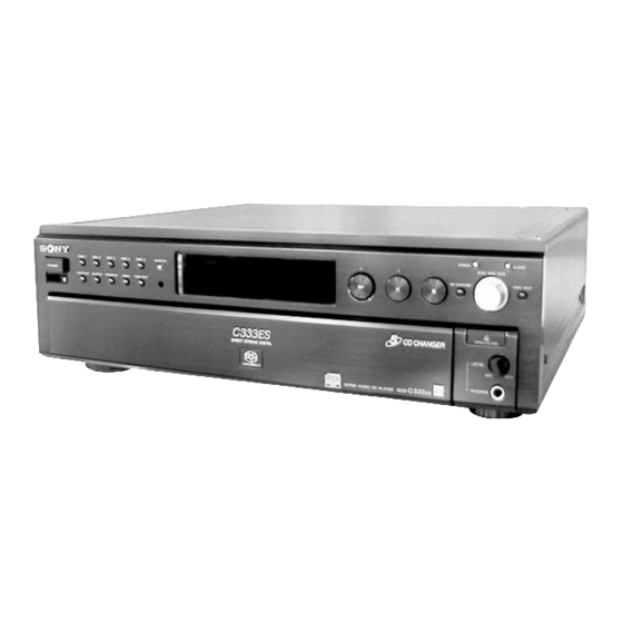
SECTION 2 GENERAL This section is extracted from instruction manual. Front Panel Parts Descriptions CHECK CLEAR DISC 1 DISC 2 DISC 3 DISC 4 DISC 5 SACD EX-CHANGE DISC SKIP POWER CONTINUE SHUFFLE PROGRAM MENU TIME/TEXT PUSH ENTER OPEN/CLOSE LEVEL PHONES 1 POWER switch (11) qs CLEAR button (20) -
Page 5: Rear Panel Parts Descriptions
1 ANALOG OUT jacks (5) 4 CONTROL A1 jack (5) Connect to an audio component using the audio Connect to the Sony audio component using the connecting cord. monaural (2P) mini-plug cord. 2 DIGITAL (CD) OUT OPTICAL connector (5) Note... -
Page 6: Disassembly
SECTION 3 DISASSEMBLY Follow the disassembly procedure in the numerical order given. Note : 3-1. COVER 3 cover 2 screw(TP) 1 two screws(TP) 1 two screws(TP) 3-2. FRONT PANEL SECTION 1 connector (CN906) 6 two screws (BVTP3 × 8) 3 connector (CN303) 2 connector (CN404) -
Page 7: Main Board
3-3. MAIN BOARD 8 two screws 1 connectors (BVTP3 × 8) (CN701) 7 two screws (BVTP3 × 8) 9 MAIN board 2 wire (flat type) (35 core) (CN503) 3 connectors (CN904) 6 connectors (CN905) 4 wire (flat type) (16 core) (CN901) 5 wire (flat type) (8 core) (CN902) -
Page 8: Cd Mechanism Deck (Cdm59-Dvbu5)
3-5. CD MECHANISM DECK (CDM59-DVBU5) 1 five screws (BVTP3 × 8) 3 sub chassis 2 five screws (BVTP3 × 8) 8 CD mechanism deck 4 three screws (CDM59-DVBU5) (BVTP3 × 8) 6 screw (BVTP3 × 8) 7 screw(BVTP3 × 8) 5 Slide the tray until the screw that fixes the table assy can be seen through around hole... -
Page 9: Optical Pick-Up Block (Khm-230Aaa/J1Np)
3-6. OPTICAL PICK-UP BLOCK (KHM-230AAA/J1NP) 3 two screws 3 two screws (PTPWH M2.6) (PTPWH M2.6) 4 optical pick-up block (KHM-230AAA/J1NP) Note: When installing the BU BU section on the chassis, set the gear (U/D) lever (lifter) in free 5 four compression springs (932) position, the gear (U/D) in UP position, and insert the shaft... -
Page 10: Tray, Sensor Board
3-8. TRAY, SENSOR BOARD 1 screw (PTPWH M2.6) 3 belt (rotary) 2 tray 5 SENSOR board 4 two screws 4 two screws (BTTP M2.6) (BTTP M2.6) 3-9. LOADING MOTOR BOARD 3 two screws (BTTP M2.6) 4 LOADING MOTOR board 1 belt (loading) 2 connector (CN13) -
Page 11: Adjusting Phase Of Swing Gear And Gear (U/D)
3-10. ADJUSTING PHASE OF SWING GEAR AND GEAR (U/D) 5 stopper washer (FR) 4 Push fully the shaft of shaft gear and align the hole shape of gear (loading B). 3 Let the swing gear through under the 6 screw chassis and engage its dowel (PTPWH M2.6) -
Page 12: Diagrams
SECTION 4 DIAGRAMS NOTE FOR PRINTED WIRING BOARDS AND SCHEMATIC DIAGRAMS Note on Printed Wiring Board: Note on Schematic Diagram: • X : parts extracted from the component side. • All capacitors are in µF unless otherwise noted. pF: µµF •... -
Page 13: Block Diagrams
SCD-C333ES 4-1. BLOCK DIAGRAMS RF SECTION OPTICAL PICK-UP BLOCK (KHM-230AAA/J1NP) RFSIN ATOP RFAC RFAC DVDRFP TO MAIN SECTION(1/2) ATON (Page 14) IC004(1/2) VC-BUFFER +3.3V • Signal Path 1.65V : SACD IC509 AVC 1.65V CD-DECODER : CD SERVO-DSP DETECTOR : DIGITAL OUT... -
Page 14: Main Section-1
SCD-C333ES MAIN SECTION-1 RF_AC TO RF/SERVO SECTION RFIN (Page 13) • Signal Path SP_DW IC704 SP_DW : SACD IC812 TO MAIN SECTION(2/2) (Page 15) BUFFER MA0 – 9 IC815 SHIFT REGISTER XHWR SDCK EXCKO1 IC706 D-RAM XHRD BD0 – F... -
Page 15: Main Section-2
SCD-C333ES MAIN SECTION-2 D0 -D7 DATA BUS DATA BUS TO MAIN SECTION(1/2) (Page 14) A0 - A7 ADDRESS BUS ADDRESS BUS TO MAIN SECTION(1/2) (Page 14) TO MAIN SECTION(1/2) (Page 14) RS-232C (JIG) D0 - D7 A0 - A6 D0 -D7 IC920 44 –... -
Page 16: Audio Section
SCD-C333ES AUDIO SECTION IC101 IC301 IC100 IC102(1/2) DIGITAL FILTER CURRENT PULSE D/A CONVERSION IC102(2/2) AUDIO FILTER J301 Q100 BUFFER ANALOG OUT MDAT L1 (–) TO RF/SERVO SECTION DATAI IN2– I01+ BCLK (Page 13) BCKI L1 (+) IN2+ I02– LRCK LRCKI L2 (+) I01–... -
Page 17: Display/Power Section
SCD-C333ES DISPLAY/POWER SECTION IC1001 FLUORESCENT INDICATOR TUBE DRIVE IC1002 DISPLAY CONTROLLER IFBSY Q1001 FL CLK (CL) SEGMENT D1002 DRIVE FL1000 XFRRST RESET FLT (CE) FLUORESCENT INDICATOR TUBE SIN1 FL DATA (DI) SOUT TO MAIN SECTION(2/2) (Page 15) IFSO0 RESET OUT... -
Page 18: Schematic Diagram Rf Section
SCD-C333ES 4-2. SCHEMATIC DIAGRAM RF SECTION • Refer to page 40 for Waveforms. -
Page 19: Printed Wiring Board Rf Section
SCD-C333ES 4-3. PRINTED WIRING BOARD RF SECTION • Refer to page 12 for Circuit Board Location. There are a few cases that the part printed on this diagram isn’t mounted in this model. • Semiconductor Location Ref. No. Location D001... -
Page 20: Printed Wiring Board Main Section (Side A)
SCD-C333ES 4-4. PRINTED WIRING BOARD MAIN SECTION (SIDE A) • Refer to page 12 for Circuit Board Location. There are a few cases that the part printed on this diagram isn’t mounted in this model. (Page 19) (Page 30) (Page 30) •... -
Page 21: Printed Wiring Board Main Section (Side B)
SCD-C333ES 4-5. PRINTED WIRING BOARD MAIN SECTION (SIDE B) • Refer to page 12 for Circuit Board Location. There are a few cases that the part printed on this diagram isn’t mounted in this model. • Semiconductor Location Ref. No. Location... -
Page 22: Schematic Diagram Main Section (1/5)
SCD-C333ES 4-6. SCHEMATIC DIAGRAM MAIN SECTION (1/5) • Refer to page 49 for IC Pin Function. PIN FUNCTION... -
Page 23: Schematic Diagram Main Section (2/5)
SCD-C333ES 4-7. SCHEMATIC DIAGRAM MAIN SECTION (2/5) • Refer to page 40 for Waveforms. • Refer to page 41 for IC Block Diagrams. • Refer to page 46 for IC Pin Function. PIN FUNCTION... -
Page 24: Schematic Diagram Main Section (3/5)
SCD-C333ES 4-8. SCHEMATIC DIAGRAM MAIN SECTION (3/5) • Refer to page 40 for Waveform. • Refer to page 41 for IC Block Diagrams. • Refer to page 48 for IC Pin Function. PIN FUNCTION... -
Page 25: Schematic Diagram Main Section (4/5)
SCD-C333ES 4-9. SCHEMATIC DIAGRAM MAIN SECTION (4/5) • Refer to page 40 for Waveform. • Refer to page 42 for IC Block Diagrams. -
Page 26: Schematic Diagram Main Section (5/5)
SCD-C333ES 4-10. SCHEMATIC DIAGRAM MAIN SECTION (5/5) • Refer to page 40 for Waveform. • Refer to page 43 for IC Block Diagrams. -
Page 27: Schematic Diagram Audio Section (1/3)
SCD-C333ES 4-11. SCHEMATIC DIAGRAM AUDIO SECTION (1/3) • Refer to page 40 for Waveforms. • Refer to page 44, 45 for IC Block Diagrams. -
Page 28: Schematic Diagram Audio Section (2/3)
SCD-C333ES 4-12. SCHEMATIC DIAGRAM AUDIO SECTION (2/3) -
Page 29: Schematic Diagram Audio Section (3/3)
SCD-C333ES 4-13. SCHEMATIC DIAGRAM AUDIO SECTION (3/3) -
Page 30: Printed Wiring Board Audio Section (Side A)
SCD-C333ES 4-14. PRINTED WIRING BOARD AUDIO SECTION (SIDE A) • Refer to page 12 for Circuit Board Location. There are a few cases that the part printed on this diagram isn’t mounted in this model. (Page 39) (Page 39) (Page 35) -
Page 31: Printed Wiring Board Audio Section (Side B)
SCD-C333ES 4-15. PRINTED WIRING BOARD AUDIO SECTION (SIDE B) • Refer to page 12 for Circuit Board Location. -
Page 32: Schematic Diagram Display Section
SCD-C333ES 4-16. SCHEMATIC DIAGRAM DISPLAY SECTION • Refer to page 45 for IC Block Diagrams. -
Page 33: Printed Wiring Board Display Section
SCD-C333ES 4-17. PRINTED WIRING BOARD DISPLAY SECTION • Refer to page 12 for Circuit Board Location. (Page 30) (Page 20) (Page 35) • Semiconductor Location Ref. No. Location D1000 D1001 D1002 D1003 B-12 IC1001 IC1002 Q1000 Q1001 Q1002 Q1004 B-12... -
Page 34: Schematic Diagram Hp Section
SCD-C333ES 4-18. SCHEMATIC DIAGRAM HP SECTION... -
Page 35: Printed Wiring Board Hp Section
SCD-C333ES 4-19. PRINTED WIRING BOARD HP SECTION • Refer to page 12 for Circuit Board Location. (Page 30) (Page 33) (Page 20) -
Page 36: Schematic Diagram Sensor Section
SCD-C333ES 4-20. SCHEMATIC DIAGRAM SENSOR SECTION • Refer to page 45 for IC Block Diagram. -
Page 37: Printed Wiring Board Sensor Section
SCD-C333ES 4-21. PRINTED WIRING BOARD SENSOR SECTION • Refer to page 12 for Circuit Board Location. MAIN BOARD (Page 20) -
Page 38: Schematic Diagram Power Section
SCD-C333ES 4-22. SCHEMATIC DIAGRAM POWER SECTION... -
Page 39: Printed Wiring Board Power Section
SCD-C333ES 4-23. PRINTED WIRING BOARD POWER SECTION • Refer to page 12 for Circuit Board Location. (Page 30) (Page 30) (Page 30) - Page 40 • Waveforms – RF Board – – MAIN Board – – AUDIO Board – 1 IC001 el (TE) (CD PLAY) 1 IC901 r; (XTAL) 6 IC801 rs (BCKD) 1 IC300 5 (Q) Approx. 4.4 Vp-p 3.4 Vp-p 4 Vp-p 100 mVp-p 20 MHz 177 ns 354 ns...
-
Page 41: Ic Block Diagrams
4-24. IC BLOCK DIAGRAMS IC809 SN74LV74APWR (MAIN BOARD) IC906 TC74VHCT32AFT (MAIN BOARD) IC908 LC35256DM-70 (MAIN BOARD) MEMORY I/O8 ADDRESS CELL ARRAY I/O7 BUFFER DECODER 512 x 512 I/O6 I/O5 I/O4 INPUT INPUT COLUMN OUTPUT DATA DATA DATA BUFFER CONTROL CONTROL BUFFER COLUMN I/O3... - Page 42 IC904 BU2500FV-E2 (MAIN BOARD)
- Page 43 IC509 CXD3008Q (MAIN BOARD) 80 79 78 77 76 75 74 73 72 71 70 69 68 67 66 LRCK XRST DIGITAL DOUT MUTE DATA DATA ASYE XLAT XLAT INTERFACE CLOK CLOK INTERFACE SENS SENS VPC0 CLOCK V16M ERROR GENERATOR SCLK CORRECTOR ATSK...
- Page 44 IC301 CXD9556AQ (AUDIO BOARD)
- Page 45 IC100, IC200 CXA8042AS (AUDIO BOARD) IC11 BA6780 (JUNCTION BOARD) I01+ IN2– VIN1 VIN2 IN2+ I02– I01– IN1+ SWITCHING I02+ IN1– FIN1 FIN2 CIRCUIT VCC2 GND2 RIN1 RIN2 VEE2 VCC1 IOUT CONSTANT REFERENCE VEE1 VREF CURRENT VOLTAGE CIRCUIT CIRCUIT VREF CONTROL VCNT CIRCUIT FBIN-...
-
Page 46: Ic Pin Function Description
4-25. IC PIN FUNCTION DESCRIPTION • MAIN BOARD IC801 CXD2751Q (DSP DECODER) Pin No. Pin Name Description XSRQ Data request signal output to the DVD CONVERTER (IC701) XSHD Header flag signal input from the DVD CONVERTER (IC701) — Power supply terminal (+3.3V) —... - Page 47 Pin No. Pin Name Description ZDFLGR Data (Rch) flag detect signal output terminal Not used (Open) 51, 52 A0, A1 Address signal output to the D-RAM (IC808) — Power supply terminal (+3.3V) — Ground terminal 55 to 63 A2 to A10 Address signal output to the D-RAM (IC808) —...
- Page 48 • MAIN BOARD IC902 CXD1095BR (I/O EXPANDER) Pin No. Pin Name Description LIM_SW Limit switch for sled servo. Not used (open) (WISE) Rotating direction. Not used (open) F_COMPL Focus Jump L signal SPCNTL1 Speed control-1. Not used (open) SPCNTL0 Speed control-0. Not used (open) TBLL TABLE MOTOR - L DIRECTION TBLR...
- Page 49 • MAIN BOARD IC701 CXD1882R (SACD DECODER) Pin No. Pin Name Description 1, 2 D5, D6 Two-way data bus with the CPU (IC901) and expander (IC902) — Ground terminal (digital system) Two-way data bus with the CPU (IC901) and expander (IC902) Address signal input from the CPU (IC901) —...
- Page 50 Pin No. Pin Name Description — Ground terminal (digital system) 62, 63 HCS0, HCS1 Not used (open) — Power supply terminal (+3.3V) (digital system) DASP Not used (pull up) 66 to 69 MDB0 to MDB3 Two-way data bus with the D-RAM (IC706) —...
- Page 51 Pin No. Pin Name Description Signal output from the charge pump for frequency comparator 133, 134 GNDA2, GNDA1 — Ground terminal (analog system) Spindle motor (M3) control signal output to the BA5912AFP (IC512) Middle point voltage (+1.65V) input terminal MDIN2 Spindle motor (M3) control signal input from the CXD3008Q (IC509) MDIN1 MDP input terminal...
-
Page 52: Servicing Notes (2)
SECTION 5 SERVICING NOTES (2) Cleaning of Optical Pick-up Lens In cleaning the lens of optical pick-up, use the air blower. Never use a cotton swab for cleaning the lens of optical pick-up, which otherwise causes a trouble. Resetting Operation at Power ON If the power is turned on with a disc loaded in the set, a sequence of operation as shown below will be performed. -
Page 53: Test Mode
3G to 16G starting from the top. 4 Grids from 5G to 6G go off. * In the SCD-C333ES that does not have the [MULTI/2CH] key, attach the dummy key to the specified position and check the 2. - Page 54 [OPEN/CLOSE] key in the TEST mode. This set automatically executes self-diagnosis and various checks by entering the test mode. Note: This set automatically makes various adjustments according to the The [OPEN/CLOSE] key is disabled immediately after the machine type of disc, thereby not requiring adjustment of the set when parts enters the TEST mode.
- Page 55 FOCUS command (2X): Focus related. (All servos must be already turned on (except command 21)) Name Description Remarks FSRCH ON/OFF The continuous vertical motion of the optical pick-up lens is turned on or Avoid a long-time use F-BIAS UP Increase focus bias Focus bias value F-BIAS DOWN Decrease focus bias...
- Page 56 TOOLS command (8X): Performs aging, reads adjusting parameters, etc. Name Description Remarks VERSION Firmware version is displayed Example: Ver 1.00 TRAY AGING Tray open-close aging is performed Number of times and eccentricity Not used for the servicing measurement Not used in this set. JITTER Jitter measurement Not used for the servicing...
- Page 57 Set Check 92. SET CHECK SET TEST START 10. TOTAL CHECK 120. MANUAL CHK 121. LOAD IN ? 0. IC&FL CHECK ? 11. AUTO CHECK ? (Not used.) 1. TOTAL CHECK ? 12. MANUAL CHK ? 122. SPIN UP ? 2.
- Page 58 6-1. IC AND FLUORESCENT DISPLAY TUBE CHECK Error display Causes (typical example) (SELF-DIAGNOSIS) PRAWN DRAM ERR 1. IC808 (D-RAM) is faulty The communication between microcomputer and main ICs (self- 2. IC801 (DSD decoder) is faulty diagnosis) and the fluorescent display tube all lit are checked. 3.
- Page 59 6-2. AUTO CHECK (AUTOMATIC VARIOUS MEASUREMENTS) The auto check is performed to check if the set operates stably. Though a checking is made automatically, whether the measured data are within the specification is evaluated by the service person. The auto check results in NG immediately, if the check itself causes an error. Setting Method of Auto Check Mode: 1.
- Page 60 Items Description Remarks HENSIN Eccentricity measurement For the CD only are measured Eccentricity (actual eccentric amount) of disc, disc pulley total • Read by dividing by 10 • 0 may be displayed if eccentricity is small (10um or less) (Due to measurement reason) SPIN DOWN TIME (msec) Time from spindle brake application to rotation stop...
- Page 61 (2) CD (Use the test disc PATD-012 or YEDS-18) Note: Measured values in check items are typical ones. Check items Specified value LOAD IN TIME (msec) Not displayed in this set. SPIN UP TIME (msec) : 1372 1700 msec or less RF/VC/FE/TE AVRG (ORG) : 98, C, 1D6, 4 RF: 80-9B, VC: 1F1-10, FE: 1d8-42, TE: 1BB-5C...
- Page 62 6-3. SACD (DL) DISC OPERATION CHECK 6-4. HYBRID DISC OPERATION CHECK (• Perform as necessary) (• Perform as necessary) The stability of the set can be checked by repeating the combined This test checks the auto adjustment time required when the disc operation of focus jump (layer 0t1, layer 1t0) and access to is switched between HD (SACD) layer and CD layer.
- Page 63 6-5. CDM59 and the Door Check Measurement of table rotation hours, tray open/close hours and panel door open close hours can be executed together with CDM59. Procedure 1. Enter the TEST mode. Turn the dial and select 59 Table Init. Press once (that enables the [OPEN/CLOSE] key.)
- Page 64 3. Press the button to turn the power off. of SCD-C333ES, the multiple discs can be placed. Even when Note: Take care not to leave the test disc in the set. the discs (CD or the SACD SL disc) of different types are The following setups are established in the SHIPPING MODE mixed, the aging test can be performed.
- Page 65 Error display is as follows. Error name, Disc type, IN SW (Sled in switch state), FOK (FOK signal state), LOCK (LOCK signal state), From (Displayed if effective), To (Displayed if effective), Aging times (Displayed in aging mode only) Display example ACCESS MOVE ERROR : SACDSL : IN SW 1 FOK 0 LOCK 0 : FROM 205663 : TO 2461601 : TIMES 5 (Error name) (Disc type) (Sled in switch, FOK, LOCK signal state) (Relative address) (Relative address)(Aging times) Display Items List:...
- Page 66 6-8. WAVEFORMS CHECK Traverse Check This set performs automatic adjustment for each disc, and there- Connection: fore the set need not be adjusted when parts are replaced, but it requires checking following the description in this section, 6-1. oscilloscope IC AND FLUORESCENT DISPLAY TUBE CHECK and 6-2. MAIN board AUTO CHECK.
- Page 67 RF Level Check CLV Jitter Check (CD only) Connection: Connection: oscilloscope oscilloscope MAIN board MAIN board (CH1) TP516 (RFCK) TP703 (RFAC) – TP517(WFCK) – TP704 (AGND) (CH2) TP808 (DG) Checking Method: Checking Method: 1. Under the condition of traverse waveform check mode in step 1.
- Page 68 Checking and Connecting Location: – MAIN Board (Component Side) – TP513 (TE) TP704 TP703 (AGND) (RFAC) TP504 (AVC) TP506 (FE) IC509 IC701 TP517 (WFCK) TP516 (RFCK) TP808 IC801 (DG)
-
Page 69: Exploded Views
SECTION 7 EXPLODED VIEWS NOTE: • -XX, -X mean standardized parts, so they may • The mechanical parts with no reference number The components identified by mark 0 or have some differences from the original one. in the exploded views are not supplied. dotted line with mark 0 are critical for safety. -
Page 70: 7-2.Front Panel Section
4-230-711-01 LID 4-230-722-01 BUTTON (PLAY) 4-951-620-01 SCREW (2.6X8), +BVTP 4-230-723-01 BUTTON (OPEN/CLOSE) 4-230-710-01 BASE, LID 4-230-718-01 BASE, PANEL 4-942-568-41 EMBLEM (NO.5), SONY 4-230-703-01 SHAFT (LIMITTER) 4-230-714-01 EMBLEM (SACD) 4-230-701-01 GEAR (LIMITTER) 4-992-539-11 KNOB(PHONE LEVEL) 4-230-704-01 SPRING (LIMITTER) 4-230-720-01 ESCUTCHEON (H.P) -
Page 71: 7-3.Main Chassis Section
7-3. MAIN CHASSIS SECTION not supplied not supplied AUDIO board (not supplied) not supplied not supplied AC board (not supplied) T102 T101 not supplied not supplied Ref. No. Part No. Description Remarks Ref. No. Part No. Description Remarks 0 106 A-4725-364-A MAIN BOARD, COMPLETE 1-783-531-31 CORD, POWER 1-757-135-11 WIRE (FLAT TYPE) (35 CORE) -
Page 72: 7-4.Cd Mechanism (Cdm59-Dvbu5) -1 Section
7-4. CD MECHANISM (CDM59-DVBU5) -1 SECTION not supplied not supplied not supplied supplied not supplied Ref. No. Part No. Description Remarks Ref. No. Part No. Description Remarks 4-224-603-01 TRAY 4-224-616-01 GEAR (RM-M) 4-218-253-01 SCREW (M2.6), +BTTP 4-224-615-01 GEAR (RM-B) 4-224-619-01 BRACKET (GUIDE) 4-225-328-01 BELT (ROTARY) 4-224-602-01 TABLE 1-676-245-11 SENSOR BOARD... -
Page 73: 7-5.Cd Mechanism (Cdm59-Dvbu5) -2 Section
7-5. CD MECHANISM (CDM59-DVBU5) -2 SECTION not supplied S200 not supplied Note : Note : The components identified by Les composants identifiés par mark 0 or dotted line with mark une marque 0 sont critiques 0 are critical for safety. pour la sécurité. -
Page 74: Electrical Parts List
SECTION 8 AC SW AUDIO ELECTRICAL PARTS LIST NOTE: • Due to standardization, replacements in the • RESISTORS When indicating parts by reference number, parts list may be different from the parts All resistors are in ohms. please include the board name. specified in the diagrams or the components METAL: metal-film resistor The components identified by mark 0 or... - Page 75 AUDIO Ref. No. Part No. Description Remarks Ref. No. Part No. Description Remarks C222 1-136-235-91 FILM 0.0091uF 3.00% 100V C346 1-163-133-00 CERAMIC CHIP 470PF C223 1-136-252-00 FILM 0.0015uF 5.00% 100V C347 1-164-695-11 CERAMIC CHIP 0.0022uF 5.00% 50V C224 1-136-252-00 FILM 0.0015uF 5.00% 100V C348 1-164-695-11 CERAMIC CHIP...
- Page 76 AUDIO Ref. No. Part No. Description Remarks Ref. No. Part No. Description Remarks C446 1-164-695-11 CERAMIC CHIP 0.0022uF 5.00% 50V < IC > C447 1-164-695-11 CERAMIC CHIP 0.0022uF 5.00% 50V C448 1-164-695-11 CERAMIC CHIP 0.0022uF 5.00% 50V IC100 8-759-371-51 IC CXA8042AS IC101 8-759-566-39 IC OPA2132UA/2K5 <...
- Page 77 AUDIO Ref. No. Part No. Description Remarks Ref. No. Part No. Description Remarks < TRANSISTOR > R219 1-259-999-11 CARBON MELF 2.2K 1/8W R220 1-260-002-11 CARBON MELF 3.3K 1/8W Q100 8-729-202-05 TRANSISTOR 2SC2873O-TE12L R221 1-260-002-11 CARBON MELF 3.3K 1/8W Q101 8-729-202-05 TRANSISTOR 2SC2873O-TE12L R222 1-260-002-11 CARBON MELF...
- Page 78 AUDIO DISPLAY Ref. No. Part No. Description Remarks Ref. No. Part No. Description Remarks R400 1-216-089-11 RES-CHIP 1/10W < DIODE > R401 1-216-025-11 RES-CHIP 1/10W R402 1-216-025-11 RES-CHIP 1/10W D1000 8-719-046-40 DIODE SEL5521C-TH8F R403 1-216-089-11 RES-CHIP 1/10W D1001 8-719-046-35 DIODE SEL5921A-TH8F R404 1-216-061-00 METAL CHIP 3.3K...
- Page 79 DISPLAY DOOR MOTOR DOOR SW JUNCTION Ref. No. Part No. Description Remarks Ref. No. Part No. Description Remarks R1038 1-216-298-00 METAL CHIP 1/10W HP BOARD R1039 1-216-073-00 METAL CHIP 1/10W ********* R1040 1-216-097-11 RES-CHIP 100K 1/10W R1041 1-216-097-11 RES-CHIP 100K 1/10W 4-962-201-01 PLATE(HP), GROUND R1042...
- Page 80 LOADING MOTOR MAIN Ref. No. Part No. Description Remarks Ref. No. Part No. Description Remarks KEY BOARD C535 1-162-966-11 CERAMIC CHIP 0.0022uF 10% ********** C536 1-125-891-11 CERAMIC CHIP 0.47uF 10.00% 10V C537 1-216-864-11 METAL CHIP 1/16W < CONNECTOR > C539 1-107-826-11 CERAMIC CHIP 0.1uF 10.00% 16V...
- Page 81 MAIN Ref. No. Part No. Description Remarks Ref. No. Part No. Description Remarks C721 1-107-826-11 CERAMIC CHIP 0.1uF 10.00% 16V C813 1-162-970-11 CERAMIC CHIP 0.01uF C722 1-164-156-11 CERAMIC CHIP 0.1uF C814 1-125-822-11 TANTALUM 10uF 20.00% 10V C723 1-164-156-11 CERAMIC CHIP 0.1uF C815 1-162-970-11 CERAMIC CHIP...
- Page 82 MAIN Ref. No. Part No. Description Remarks Ref. No. Part No. Description Remarks < CONNECTOR > FL901 1-234-177-21 FILTER, CHIP EMI FL902 1-234-177-21 FILTER, CHIP EMI CN503 1-784-883-21 CONNECTOR,FFC(LIF(NON-ZIF))35P FL903 1-234-177-21 FILTER, CHIP EMI CN701 1-794-606-41 PIN, CONNECTOR (PC BPARD 9P FL904 1-234-177-21 FILTER, CHIP EMI * CN801...
- Page 83 MAIN Ref. No. Part No. Description Remarks Ref. No. Part No. Description Remarks < RESISTOR > R608 1-218-716-11 METAL CHIP 0.5% 1/16W R609 1-216-864-11 METAL CHIP 1/16W R501 1-216-833-11 METAL CHIP 1/16W R610 1-216-864-11 METAL CHIP 1/16W R502 1-216-833-11 METAL CHIP 1/16W R611 1-218-724-11 METAL CHIP...
- Page 84 MAIN Ref. No. Part No. Description Remarks Ref. No. Part No. Description Remarks R728 1-218-716-11 METAL CHIP 0.5% 1/16W R813 1-216-801-11 METAL CHIP 1/16W R729 1-216-864-11 METAL CHIP 1/16W R814 1-216-801-11 METAL CHIP 1/16W R730 1-216-801-11 METAL CHIP 1/16W R815 1-216-801-11 METAL CHIP 1/16W R731...
- Page 85 MAIN REMOTE SENSOR Ref. No. Part No. Description Remarks Ref. No. Part No. Description Remarks R922 1-216-801-11 METAL CHIP 1/16W R994 1-216-789-11 METAL CHIP 1/16W R923 1-216-833-11 METAL CHIP 1/16W R995 1-218-712-11 METAL CHIP 6.8K 0.5% 1/16W R924 1-216-833-11 METAL CHIP 1/16W R998 1-216-864-11 METAL CHIP...
- Page 86 SENSOR Ref. No. Part No. Description Remarks Ref. No. Part No. Description Remarks C037 1-115-416-11 CERAMIC CHIP 0.001uF 5.00% 25V < RESISTOR > C038 1-126-206-11 ELECT CHIP 100uF 6.3V C039 1-107-826-11 CERAMIC CHIP 0.1uF 10.00% 16V R001 1-216-864-11 METAL CHIP 1/16W C040 1-162-970-11 CERAMIC CHIP...
- Page 87 SENSOR Ref. No. Part No. Description Remarks Ref. No. Part No. Description Remarks < DIODE > 8-749-924-18 PHOTO INTERRUPTER RPI-1391 (TABLE SENSOR) 8-749-017-45 SENSOR, PHONT RPR-220C1N (DISC SENSOR) < RESISTOR > 1-249-416-11 CARBON 1/4W F 1-249-407-11 CARBON 1/4W F 1-249-429-11 CARBON 1/4W ************************************************************ MISCELLANEOUS...
- Page 88 SCD-C333ES Sony Corporation 9-929-551-11 2000J1613-1D Audio Entertainment Group Printed in Japan ©2000.10 Published by General Engineering Dept.
Need help?
Do you have a question about the SCD-C333ES and is the answer not in the manual?
Questions and answers