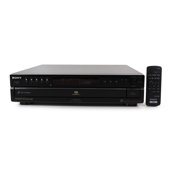
Sony SCD-CE595 Service Manual
Hide thumbs
Also See for SCD-CE595:
- Operating instructions manual (100 pages) ,
- Specifications (2 pages) ,
- Documentation update (2 pages)
Table of Contents
Advertisement
SERVICE MANUAL
Ver. 1.3 2006.08
When a Super Audio CD is played
Playing frequency range
Frequency response
Dynamic range
Total harmonic distortion rate
Wow and flutter
When a CD is played
Frequency response
Dynamic range
Total harmonic distortion rate
Wow and flutter
Output connector
ANALOG
5.1CH OUT
DIGITAL
(CD) OUT
OPTICAL*
* Output only the audio signals of the CD
Sony Corporation
9-879-006-04
Home Audio Division
2006H16-1
Published by Sony Techno Create Corporation
© 2006.08
SPECIFICATIONS
2 Hz to 100 kHz
2 Hz to 40 kHz (–3 dB)
100 dB or more
0.0035 % or less
Value of measurable limit
(±0.001 % W. PEAK) or
less
2 Hz to 20 kHz
96 dB or more
0.0039 % or less
Value of measurable limit
(±0.001 % W. PEAK) or
less
Jack type Output
Load
level
impedance
Phono
2 Vrms (at
Over 10
jacks
50 kilohms)
kilohms
Square
–18 dBm
(Light
optical
emitting
output
wave length:
connector
660 nm)
SCD-CE595
Model Name Using Similar Mechanism
CD Mechanism Type
Optical Pick-up Name
General
Laser
Power requirements
US, Canadian:
AEP, UK:
Power consumption
Dimensions (w/h/d)
Mass (approx.)
Supplied accessories
Audio connecting cord
Remote commander
Battery
Design and specifications are subject to change
without notice.
SUPER AUDIO CD PLAYER
US Model
Canadian Model
AEP Model
UK Model
NEW
CDM79C-DVBU51
DBU-3
Semiconductor laser
(Super Audio CD: λ = 650
nm) (CD: λ = 780 nm)
Emission duration:
continuous
1
20 V AC, 60 Hz
230 V AC, 50/60 Hz
15 W
×
×
430
110
420 mm incl.
projecting parts
5.5 kg
×
Red and White
2 (1)
RM-SX800 (1)
R6 (size-AA) (2)
Advertisement
Table of Contents

Related Manuals for Sony SCD-CE595


Summary of Contents for Sony SCD-CE595
- Page 1 (Light (CD) OUT optical emitting OPTICAL* output wave length: connector 660 nm) * Output only the audio signals of the CD SUPER AUDIO CD PLAYER Sony Corporation 9-879-006-04 Home Audio Division 2006H16-1 Published by Sony Techno Create Corporation © 2006.08...
-
Page 2: Table Of Contents
THE PARTS LIST ARE CRITICAL TO SAFE OPERATION. FONCTIONNEMENT. NE REMPLACER CES COM- POSANTS REPLACE THESE COMPONENTS WITH SONY PARTS WHOSE QUE PAR DES PIÈCES SONY DONT LES NUMÉROS SONT PART NUMBERS APPEAR AS SHOWN IN THIS MANUAL OR DONNÉS DANS CE MANUEL OU DANS LES SUPPLÉMENTS IN SUPPLEMENTS PUBLISHED BY SONY. -
Page 3: Servicing Notes
SCD-CE595 SECTION 1 SERVICING NOTES SAFETY CHECK-OUT MODEL IDENTIFICATION – Back Panel – After correcting the original service problem, perform the following safety check before releasing the set to the customer: Check the antenna terminals, metal trim, “metallized” knobs, screws, and all other exposed metal parts for AC leakage. -
Page 4: General
SCD-CE595 SECTION 2 GENERAL This section is extracted from instruction manual. Front Panel 5 6 7 8 9 q; A POWER switch (9) O TIME/TEXT button (11) B DISC 1-5 buttons (9, 14) Each time you press the button, the playing time of the track, the remaining time of the disc, or TEXT Press to select the disc directly. - Page 5 SCD-CE595 A CD1/2 (command mode) switch (8) Remote Select the command mode. B CONTINUE button (9, 14) Press to resume Continuous Play from Shuffle Play or Program Play. SHUFFLE button (14) PROGRAM button (14) C TIME/TEXT button (11) Each time you press the button, the playing time of the track, the remaining time of the disc, or TEXT information appears in the display.
-
Page 6: Test Mode
SCD-CE595 SECTION 3 TEST MODE 1. Setting Methed of Test Mode 4. Key Check Press three buttons m , [PUSH ENTER] and [POWER] simulta- Procedure: neously, The test mode becomes active. Then all segments of the 1. In the key check mode, the fluorecent indicator displays “KEY fluorecent indicator tube are turned on. -
Page 7: Diagrams
SCD-CE595 SECTION 4 DIAGRAMS NOTE FOR PRINTED WIRING BOARDS AND SCHEMATIC DIAGRAMS • Waveforms – RF Board – – MAIN Board – – DISPLAY Board – Note on Printed Wiring Board: Note Schematic Diagrams. • All capacitors are in µF unless otherwise noted. (p: pF) •... -
Page 8: Block Diagram
SCD-CE595 4-1. BLOCK DIAGRAMS OPTICAL PICK-UP BLOCK IC706 DIGITAL SERVO, IC001 IC330 RF AMP DIGITAL SIGNAL PROCESSOR 6,14 OPTICAL OUT DIGITAL D OUT RFIP SIGO RFAC DOUT958 OPTICAL PCMD1 96 CDBCK 95 IC200 CDLRCK 94 IC400(1/2) J351(1/3) DSAL 83 DSAR 84... -
Page 9: Printed Wiring Board - Rf Section
SCD-CE595 • See page 7 for Circuit Boards Location. 4-2. PRINTED WIRING BOARD — RF SECTION — :Uses unleaded solder. OPTICAL R018 PICK-UP R055 R054 BLOCK R053 C036 R052 (DBU-3) C008 C011 C007 C047 R005 C006 IC001 R006 R038 C005... -
Page 10: Schematic Diagram - Rf Section
SCD-CE595 • See page 7 for Waveforms. 4-3. SCHEMATIC DIAGRAM — RF SECTION — C011 0.01 C001 0.01 C004 6.3V C027 0.01 C002 0.01 C044 C039 0.01 CN001 JL003 JL004 C015 R045 R009 JW001 0.0047 JL005 C016 0.0047 JW002 JL006... -
Page 11: Printed Wiring Board - Main Section
SCD-CE595 • See page 7 for Circuit Boards Location. 4-4. PRINTED WIRING BOARD — MAIN SECTION — :Uses unleaded solder. DISPLAY BOARD CN801 (Page 16) PT BOARD C932 CN102 C305 R961 IC950 IC985 C303 (Page 16) ETP910 D936 C931 C961... -
Page 12: Schematic Diagram - Main Section (1/4)
SCD-CE595 • See page 7 for Waveforms. 4-5. SCHEMATIC DIAGRAM — MAIN SECTION (1/4) — C754 C789 CN702 C714 C706 C755 C757 C746 STP702 C751 CL724 R783 100p C733 C745 0.047 CL723 SL798 IC703 RB604 4.7k SL897 C771 CL877 SL896... -
Page 13: Schematic Diagram - Main Section (2/4)
SCD-CE595 • See page 20 for IC Block Diagrams. • See page 20 for IC Pin Function Description. 4-6. SCHEMATIC DIAGRAM — MAIN SECTION (2/4) — CN703 FB703 FB710 RB612 RB601 RB607 RB606 FL606 C721 C713 100 16V C715 R734... -
Page 14: Schematic Diagram - Main Section (3/4)
SCD-CE595 4-7. SCHEMATIC DIAGRAM — MAIN SECTION (3/4) — CL712 CL727 CL713 STP701 C716 C709 CL711 CL728 CL729 TABLE_GND IC710 BA6956AN R861 R878 270k 470k 0 9.3 C815 R848 R851 C825 0.015 2.2K 0.0015 C808 D703 C814 R858 UDZSTE-175.1B 0.01 0.22... -
Page 15: Schematic Diagram - Main Section (4/4)
SCD-CE595 • See page 7 for Waveforms. 4-8. SCHEMATIC DIAGRAM — MAIN SECTION (4/4) — IC985 BA12FP-E2 C934 D936 C933 C932 1SR154-400TE25 D960 DAN202UT106 D937 C953 C954 C935 1SR154-400TE25 1000 D933 D931 1SR154-400TE25 1SR154-400TE25 C901 0.01 D932 IC950 C931 1SR154-400TE25... -
Page 16: Printed Wiring Board - Display Section
SCD-CE595 • See page 7 for Circuit Boards Location. 4-9. PRINTED WIRING BOARD — DISPLAY SECTION — :Uses unleaded solder. MAIN BOARD CN901 (Page 11) C891 S891 C101 • Semiconductor POWER AC IN Location Ref. No. Location T101 IC801 G-14... -
Page 17: Schematic Diagram - Display Section
SCD-CE595 • See page 7 for Waveforms. 4-10. SCHEMATIC DIAGRAM — DISPLAY SECTION — C820 0.01 25V KEY 0 C819 0.01 S852 EXCHANGE S853 CN805 DISCSKIP R832 R874 R873 R872 R871 4.7k 2.2k 2.2k R841 R842 R843 R844 R845 2.2k 2.2k... -
Page 18: Printed Wiring Board - Md-94 Board Section
SCD-CE595 • See page 7 for Circuit Boards Location. 4-11. PRINTED WIRING BOARD — MD-94 BOARD SECTION — :Uses unleaded solder. M001 TURN TABLE MOTOR SE-130 BOARD CN102 PH101 PH102 CN101 (13) MAIN BOARD CN704 (Page 11) MD-94 BOARD CN001... -
Page 19: Schematic Diagram - Md-94 Board Section
SCD-CE595 4-12. SCHEMATIC DIAGRAM — MD-94 BOARD SECTION — CN001 CN003 CN004 CN704 S001 CN002 CN102 CN101 M001 PH101 RPR-220C1N PH102 RPI-392 SCD-CE595... - Page 20 SCD-CE595 • IC Block Diagrams • IC Pin Function Description • MAIN BOARD IC705 HD6432238RN51TEV (SYSTEM CONTROLLER) – MAIN Board – Pin No. Pin Name Description IC701 M51957BFP-600C IC702 BR9040F-WF2 SDATA DAC Data output to the DAC (IC200) SCLK DAC...
- Page 21 SCD-CE595 Pin No. Pin Name Description Flash writing Enable Muving mode control 2 — Not used (open) — Not used (open) Reed sycle signal Write sycle signal XWRST Waltz reset signal output XWAIT Bus sycle wait signal input SMUTE Waltz smute signal output...
-
Page 22: Exploded Views
SCD-CE595 Ver. 1.3 SECTION 5 EXPLODED VIEWS NOTE: • -XX and -X mean standardized parts, so they • The mechanical parts with no reference The components identified by mark 0 or may have some difference from the original number in the exploded views are not supplied. -
Page 23: Front Panel Section
SCD-CE595 5-2. FRONT PANEL SECTION not supplied not supplied not supplied not supplied Ref. No. Part No. Description Remark Ref. No. Part No. Description Remark X-4956-434-1 PANEL ASSY, FRONT (US,CND) 4-255-244-01 BUTTON, POWER X-4956-435-1 PANEL ASSY, FRONT (AEP,UK) A-4752-651-A DISPLAY BOARD, COMPLETE... -
Page 24: Chassis Section
SCD-CE595 5-3. CHASSIS SECTION CD mechanism section (CDM79C-DVBU51) not supplied not supplied T101 Ref. No. Part No. Description Remark Ref. No. Part No. Description Remark X-2022-049-1 FOOT ASSY 4-951-620-01 SCREW (2.6X8), +BVTP 4-977-358-01 CUSHION 0 T101 1-443-286-11 TRANSFORMER, POWER (US,CND) -
Page 25: Cd Mechanism Section (1) (Cdm79C-Dvbu51)
SCD-CE595 Ver. 1.2 5-4. CD MECHANISM SECTION (1) (CDM79C-DVBU51) supplied supplied supplied CD mechanism section (2) (CDM79C-DVBU51) Ref. No. Part No. Description Remark Ref. No. Part No. Description Remark 3-074-737-01 PLATE (GUIDE) 3-074-717-01 TRAY A-6060-642-A SE-130 BOARD, COMPLETE 4-218-252-52 SCREW (+PTPWH M2.6), FLOATING... - Page 26 SCD-CE595 5-5. CD MECHANISM SECTION (2) (CDM79C-DVBU51) supplied supplied RE901 not supplied M901 not supplied not supplied Ref. No. Part No. Description Remark Ref. No. Part No. Description Remark 4-218-252-52 SCREW (+PTPWH M2.6), FLOATING 4-981-923-01 SCREW (M), STEP 3-074-744-01 GEAR (LOADING A)
-
Page 27: Electrical Parts List
SCD-CE595 SECTION 6 ELECTRICAL PARTS LIST DISPLAY NOTE: • Due to standardization, replacements in the • RESISTORS When indicating parts by reference number, parts list may be different from the parts All resistors are in ohms. please include the board name. - Page 28 SCD-CE595 DISPLAY MAIN Ref. No. Part No. Description Remark Ref. No. Part No. Description Remark S853 1-762-875-21 SWITCH, KEYBOARD (DISC SKIP) C202 1-126-205-11 ELECT CHIP 47uF 6.3V S855 1-478-268-11 ENCODER, ROTARY C206 1-115-156-11 CERAMIC CHIP (. AMS >)(PUSH ENTER) C208...
- Page 29 SCD-CE595 MAIN Ref. No. Part No. Description Remark Ref. No. Part No. Description Remark C706 1-164-156-11 CERAMIC CHIP 0.1uF C778 1-164-156-11 CERAMIC CHIP 0.1uF C779 1-164-156-11 CERAMIC CHIP 0.1uF C709 1-126-246-11 ELECT CHIP 220uF C780 1-164-156-11 CERAMIC CHIP 0.1uF C711 1-164-156-11 CERAMIC CHIP 0.1uF...
- Page 30 SCD-CE595 MAIN Ref. No. Part No. Description Remark Ref. No. Part No. Description Remark CN703 1-793-989-21 CONNECTOR, FFC/FPC 13P < JACK > CN901 1-784-924-11 PIN, CONNECTOR 8P J351 1-785-536-11 JACK, PIN 6P (5.1CH OUT)(ANALOG) < DIODE > < TRANSISTOR >...
- Page 31 SCD-CE595 MAIN MD-94 Ref. No. Part No. Description Remark Ref. No. Part No. Description Remark R564 1-216-827-11 METAL CHIP 3.3K 1/10W R963 1-216-821-11 METAL CHIP 1/10W R567 1-216-845-11 METAL CHIP 100K 1/10W R971 1-216-833-11 METAL CHIP 1/10W R568 1-216-815-11 METAL CHIP...
- Page 32 SCD-CE595 POWER SW Ref. No. Part No. Description Remark Ref. No. Part No. Description Remark 1-862-176-11 POWER SW BOARD C040 1-164-217-11 CERAMIC CHIP 150PF C043 1-107-826-11 CERAMIC CHIP 0.1uF **************** C044 1-124-779-00 ELECT CHIP 10uF < CAPACITOR > C046 1-107-726-91 CERAMIC CHIP 0.01uF...
- Page 33 SCD-CE595 SE-130 Ref. No. Part No. Description Remark A-6060-642-A SE-130 BOARD ************ < CONNECTOR > CN101 1-750-243-11 SOCKET, CONNECTOR 6P CN102 1-573-383-11 PIN, CONNECTOR (PC BOARD) 2P < PHONT SENSOR > PH101 8-749-017-45 SENSOR, PHONT RPR-220C1N PH102 6-600-072-01 IC RPI-392...
- Page 34 SCD-CE595 MEMO...
- Page 35 SCD-CE595 US Model Canadian Model SERVICE MANUAL AEP Model UK Model Ver. 1.1 2005.05 SUPPLEMENT-1 Subject: TEST MODE and ELECTRICAL ADJUSTMENT 9-879-006-81...
- Page 36 SCD-CE595 SECTION 1 TEST MODE 1. DIAG MODE of The Test Mode While press [MENU] and [PUSH ENTER] buttons, press the [POWER] button to turn the power on and enter the Test Mode and display “DIAG MODE”. 2. Operating The Test Mode Procedure: 1.
- Page 37 SCD-CE595 SECTION 2 ELECTRICAL ADJUSTMENTS GENERAL DESCRIPTION Procedure: After parts to the circuit (OPTICAL PICK-UP (DBU-3), RF 1. Press the Z button. BOARD, MAIN BOARD, EEPROM (IC702), MASTERCOM 2. Insert SACD hybrid disc (market disc). (IC705), DSP (IC706), so on) are replaced, readjusting is necessary.
-
Page 38: Revision History
SCD-CE595 REVISION HISTORY Clicking the version allows you to jump to the revised page. Also, clicking the version at the upper right on the revised page allows you to jump to the next revised page. Ver. Date Description of Revision 2004.06...
Need help?
Do you have a question about the SCD-CE595 and is the answer not in the manual?
Questions and answers