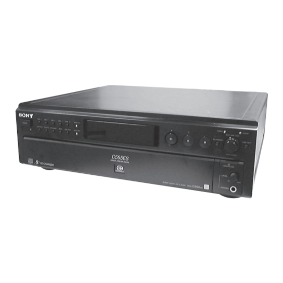
Sony SCD-C555ES Service Manual
Super audio cd player
Hide thumbs
Also See for SCD-C555ES:
- Operating instructions manual (72 pages) ,
- Dimensions (1 page) ,
- Limited warranty (1 page)
Table of Contents
Advertisement
SERVICE MANUAL
Ver 1.0 2001. 03
When a super audio CD is played
Playing frequency range 2 Hz to 100 kHz
Frequency response
Dynamic range
Total harmonic distortion rate
Wow and flutter
When a CD is played
Frequency response
Dynamic range
Total harmonic distortion rate
Wow and flutter
Output connector
Jack type
ANALOG OUT
Phono
jacks
Square
DIGITAL (CD)
OUT OPTICAL*
optical
output
connector
Coaxial
DIGITAL (CD)
output
OUT COAXIAL*
connector
PHONES
Stereo
phone jack
*Output only the audio signals of the CD
Sony Corporation
9-873-872-11
2001C1600-1
Audio Entertainment Group
© 2001.3
General Engineering Dept.
SCD-C555ES
SPECIFICATIONS
2 Hz to 50 kHz (–3 dB)
105 dB or more
0.0015 % or less
Value of measurable limit (±0.001 %
W. PEAK) or less
2 Hz to 20 kHz
99 dB or more
0.002 % or less
Value of measurable limit (±0.001 %
W. PEAK) or less
Output level
Load impedance
2 Vrms
Over 10 kilohms
(at 50 kilohms)
–18 dBm
Light emitting
(
)
wave length:
660 nm
0.5 Vp-p
75 ohms
32 ohms
10 mW
Model Name Using Similar Mechanism
CD Mechanism Type
Optical Pick-up Type
General
Laser
Semiconductor laser (λ = 780 nm)
Emission duration: continuous
Laser radiant power:
5.47 uW at 650 nm
*These output is the value measured at a distance of about
200mm from the objective lens surface on the optical pick-up.
Power requirements
120 V AC, 60 Hz
Power consumption
38 W
430 × 138 × 409 mm
Dimensions (w/h/d)
(17 × 5 1/2 × 16 1/8 in.)
incl. projecting parts
Mass (approx.)
11.0 kg (24 lbs 5 oz.)
Supplied accessories
• Audio connecting cord
phono jack × 2 (Red and White) y phono jack × 2 (Red
and White) (2)
phono jack × 1 (Black) y phono jack × 1 (Black) (2)
• Monaural (2P) mini-plug cord (1) (Connecting cord for
CONTROL A1 ) (supplied for Canadian models only)
• Remote commander (remote) RM-SC500 (1)
• R06 (size-AA) batteries (2)
Design and specifications are subject to change without notice.
SUPER AUDIO CD PLAYER
US Model
Canadian Model
NEW
CDM59A
KHM-230AAA/J1NP
Advertisement
Table of Contents

Subscribe to Our Youtube Channel
Related Manuals for Sony SCD-C555ES


Summary of Contents for Sony SCD-C555ES
- Page 1 SCD-C555ES SERVICE MANUAL US Model Canadian Model Ver 1.0 2001. 03 Model Name Using Similar Mechanism CD Mechanism Type CDM59A Optical Pick-up Type KHM-230AAA/J1NP SPECIFICATIONS When a super audio CD is played General Playing frequency range 2 Hz to 100 kHz Laser Semiconductor laser (λ...
-
Page 2: Table Of Contents
DIAGRAMMES SCHÉMATIQUES ET LA LISTE DES PIÈCES SONT 8. ELECTRICAL PARTS LIST ........79 CRITIQUES POUR LA SÉCURITÉ DE FONCTIONNEMENT. NE REMPLACER CES COMPOSANTS QUE PAR DES PIÈCES SONY DONT LES NUMÉROS SONT DONNÉS DANS CE MANUEL OU DANS LES SUPPLÉMENTS PUBLIÉS PAR SONY. -
Page 3: Servicing Notes
SCD-C555ES SECTION 1 SERVICING NOTES (1) When the bottom plate is removed, the RF board can be checked. NOTES ON HANDLING THE OPTICAL PICK-UP BLOCK OR BASE UNIT eleven screws (BVTP3 × 8) The laser diode in the optical pick-up block may suffer electrostatic break-down because of the potential difference generated by the charged electrostatic load, etc. -
Page 4: General
SCD-C555ES SECTION 2 GENERAL This section is extracted from instruction manual. Front Panel Parts Descriptions CHECK CLEAR DISC 1 DISC 2 DISC 3 DISC 4 DISC 5 SACD EX-CHANGE DISC SKIP POWER CONTINUE SHUFFLE PROGRAM MENU TIME/TEXT MULTI/2CH PUSH ENTER... -
Page 5: Rear Panel Parts Descriptions
2 ANALOG 5.1CH OUT jacks (5) 5 CONTROL A1 jacks (7, 31) Connect to an amplifier equipped with the 5.1CH Connect to a Sony audio component using the input jacks (Multi-channel amplifier, AV amplifier, monaural (2P) mini-plug cord. etc.) using the audio connecting cords. -
Page 6: Disassembly
SCD-C555ES SECTION 3 DISASSEMBLY Case Front panel section Main board Audio board D-Power, I/O board Table assy CD mechanism deck (CDM59-DVBU5) Optical pick-up block (KHM-230AAA/J1NP) Tray, sensor board Loading motor board Note : Follow the disassembly procedure in the numerical order given. -
Page 7: Main Board
SCD-C555ES 3-3. MAIN BOARD 8 two screws 1 connector (BVTP3 × 8) (CN701) 7 two screws (BVTP3 × 8) 9 MAIN board 2 wire (flat type) (35 core) (CN503) 6 connector 3 connector (CN905) (CN904) 5 wire (flat type) (19 core) -
Page 8: D-Power, I/O Board
SCD-C555ES 3-5. D-POWER, I/O BOARD 6 two screws 3 four screws (BVTP3 × 8) (BVTP3 × 8) 1 Connector 7 I/O board (CN401) 2 Connector 5 seven screws (CN400) (BVTP3 × 8) 4 D-POWER board 3-6. CD MECHANISM DECK (CDM59-DVBU5) 1 five screws (BVTP3 ×... -
Page 9: Optical Pick-Up Block (Khm-230Aaa/J1Np)
SCD-C555ES 3-7. OPTICAL PICK-UP BLOCK (KHM-230AAA/J1NP) 3 two screws 3 two screws (PTPWH M2.6) (PTPWH M2.6) 4 optical pick-up block (KHM-230AAA/J1NP) Note: When installing the BU BU section on the chassis, set the gear (U/D) lever (lifter) in free 5 four compression springs... -
Page 10: Tray, Sensor Board
SCD-C555ES 3-9. TRAY, SENSOR BOARD 1 screw (PTPWH M2.6) 3 belt (rotary) 2 tray 5 SENSOR board 4 two screws 4 two screws (BTTP M2.6) (BTTP M2.6) 3-10. LOADING MOTOR BOARD 3 two screws (BTTP M2.6) 4 LOADING MOTOR board... -
Page 11: Adjusting Phase Of Swing Gear And Gear (U/D)
SCD-C555ES 3-11. ADJUSTING PHASE OF SWING GEAR AND GEAR (U/D) 5 stopper washer (FR) 4 Push fully the shaft of gear (shaft) and align the hole shape of gear (loading B). 3 Let the swing gear through under the 6 screw... -
Page 12: Diagrams
SCD-C555ES SECTION 4 DIAGRAMS NOTE FOR PRINTED WIRING BOARDS AND SCHEMATIC DIAGRAMS Note on Printed Wiring Board: Note on Schematic Diagram: • All capacitors are in µF unless otherwise noted. pF: µµF • X : parts extracted from the component side. -
Page 13: Block Diagrams
SCD-C555ES 4-1. BLOCK DIAGRAMS RF/SERVO SECTION OPTICAL PICK-UP BLOCK (KHM-230AAA/J1NP) RFSIN ATOP RFAC RFAC DVDRFP TO MAIN SECTION(1/2) ATON (Page 14) IC004(1/2) VC-BUFFER +3.3V • Signal Path 1.65V : SACD IC509 AVC 1.65V CD-DECODER : CD SERVO-DSP DETECTOR : DIGITAL OUT... -
Page 14: Main Section-1
SCD-C555ES MAIN SECTION-1 RF_AC IC810 TO RF/SERVO SECTION RFIN (Page 13) RF-BUFFER RF_AC 126 WARFI DSAL MA0 – 9 DSAL DSI1 DSAL TO AUDIO SECTION IC812 (Page 16) DSAR DSAR DSI2 BUFFER DSAR DSAC DSAC DSI3 DSAC IC706 DSASW DSALFE... -
Page 15: Main Section-2
SCD-C555ES MAIN SECTION-2 D0 -D7 DATA BUS DATA BUS TO MAIN SECTION(1/2) (Page 14) A0 - A7 ADDRESS BUS ADDRESS BUS TO MAIN SECTION(1/2) (Page 14) TO MAIN SECTION(1/2) (Page 14) RS-232C (JIG) 89 – 96 14 – 21 44 – 46 28 –... -
Page 16: Audio Section
SCD-C555ES AUDIO SECTION IC307 HEADPHONE RV1101 PHONE LEVEL J1101 IC306 PHONES COUNTER IC303 Q151 256FS 128FS MUTING 64FS TO MAIN SECTION(1/2) (Page 14) X301 11.2896MHz Q251 MUTING Q362 MUTING CONTROL J302 Q361 AMUTE Q360 RELAY 2CH OUT SWITCH DRIVE IC301... -
Page 17: Display/Power Section
SCD-C555ES DISPLAY/POWER SECTION IC1001 FLUORESCENT INDICATOR TUBE DRIVE IC1002 DISPLAY CONTROLLER IFBUSY Q1001 FL CLK (CL) SEGMENT DRIVE D1002 FL1000 XFRRST RESET FLT (CE) FLUORESCENT INDICATOR TUBE SIN1 FL DATA (DI) TO MAIN SECTION(2/2) SOUT (Page 15) IFSO0 RESET OUT... -
Page 18: Schematic Diagram Rf Section
SCD-C555ES 4-2. SCHEMATIC DIAGRAM RF SECTION • Refer to page 40 for Waveforms. IC B/D 390p... -
Page 19: Printed Wiring Board Rf Section
SCD-C555ES 4-3. PRINTED WIRING BOARD RF SECTION • Refer to page 12 for Circuit Board Location. There are a few cases that the part printed on this diagram isn’t mounted in this model. • Semiconductor Location Ref. No. Location D001... -
Page 20: Printed Wiring Board Main Section (Side A)
SCD-C555ES 4-4. PRINTED WIRING BOARD MAIN SECTION (SIDE A) • Refer to page 12 for Circuit Board Location. There are a few cases that the part printed on this diagram isn’t mounted in this model. • Semiconductor Location Ref. No. Location... -
Page 21: Printed Wiring Board Main Section (Side B)
SCD-C555ES 4-5. PRINTED WIRING BOARD MAIN SECTION (SIDE B) • Refer to page 12 for Circuit Board Location. There are a few cases that the part printed on this diagram isn’t mounted in this model. • Semiconductor Location Ref. No. Location... -
Page 22: Schematic Diagram Main Section (1/5)
SCD-C555ES 4-6. SCHEMATIC DIAGRAM MAIN SECTION (1/5) • Refer to page 49 for IC Pin Function. IC B/D IC B/D... -
Page 23: Schematic Diagram Main Section (2/5)
SCD-C555ES 4-7. SCHEMATIC DIAGRAM MAIN SECTION (2/5) • Refer to page 40 for Waveforms. • Refer to page 41 for IC Block Diagrams. • Refer to page 46 for IC Pin Function. -
Page 24: Schematic Diagram Main Section (3/5)
SCD-C555ES 4-8. SCHEMATIC DIAGRAM MAIN SECTION (3/5) • Refer to page 40 for Waveform. • Refer to page 41 for IC Block Diagrams. • Refer to page 48 for IC Pin Function. IC B/D... -
Page 25: Schematic Diagram Main Section (4/5)
SCD-C555ES 4-9. SCHEMATIC DIAGRAM MAIN SECTION (4/5) • Refer to page 40 for Waveform. • Refer to page 42 for IC Block Diagrams. IC B/D... -
Page 26: Schematic Diagram Main Section (5/5)
SCD-C555ES 4-10. SCHEMATIC DIAGRAM MAIN SECTION (5/5) • Refer to page 40 for Waveform. • Refer to page 43 for IC Block Diagrams. IC B/D... -
Page 27: Schematic Diagram Audio Section (1/2)
SCD-C555ES 4-11. SCHEMATIC DIAGRAM AUDIO SECTION (1/2) • Refer to page 40 for Waveforms. • Refer to page 44, 45 for IC Block Diagrams. (Page 31) (Page 31) (Page 31) -
Page 28: Schematic Diagram Audio Section (2/2)
SCD-C555ES 4-12. SCHEMATIC DIAGRAM AUDIO SECTION (2/2) (Page 31) IC B/D (Page 31) -
Page 29: Schematic Diagram D-Power Section
SCD-C555ES 4-13. SCHEMATIC DIAGRAM D-POWER SECTION... -
Page 30: Printed Wiring Board Audio Section
SCD-C555ES 4-14. PRINTED WIRING BOARD AUDIO SECTION • Refer to page 12 for Circuit Board Location. There are a few cases that the part printed on this diagram isn’t mounted in this model. (Page 39) IC302 IC2302 IC1302 IC306 IC1301... -
Page 31: Printed Wiring Board
SCD-C555ES 4-15. PRINTED WIRING BOARD IN OUT/D-POWER SECTION 4-16. SCHEMATIC DIAGRAM IN OUT SECTION • Refer to page 12 for Circuit Board Location. IN OUT BOARD • Semiconductor Location IC 395 Ref. No. Location D363 D364 IC395 D365 D381 IC395... -
Page 32: Schematic Diagram Display Section
SCD-C555ES 4-17. SCHEMATIC DIAGRAM DISPLAY SECTION • Refer to page 45 for IC Block Diagrams. IC B/D... -
Page 33: Printed Wiring Board
SCD-C555ES 4-18. PRINTED WIRING BOARD DISPLAY SECTION • Refer to page 12 for Circuit Board Location. IC1002 IC1001 D-POWER BOARD (Page 31) (Page 20) (Page 35) IC1000 • Semiconductor Location Ref. No. Location D1000 D1001 D1002 D1003 B-12 IC1001 IC1002... -
Page 34: Schematic Diagram Hp Section
SCD-C555ES 4-19. SCHEMATIC DIAGRAM HP SECTION AUDIO BOARD (1/2) (Page 27) -
Page 35: Printed Wiring Board Hp Section
SCD-C555ES 4-20. PRINTED WIRING BOARD HP SECTION • Refer to page 12 for Circuit Board Location. (Page 30) (Page 33) (Page 20) -
Page 36: Schematic Diagram
SCD-C555ES 4-21. SCHEMATIC DIAGRAM SENSOR SECTION • Refer to page 45 for IC Block Diagram. IC B/D... -
Page 37: Printed Wiring Board Sensor Section
SCD-C555ES 4-22. PRINTED WIRING BOARD SENSOR SECTION • Refer to page 12 for Circuit Board Location. MAIN BOARD (Page 20) IC11... -
Page 38: Schematic Diagram
SCD-C555ES 4-23. SCHEMATIC DIAGRAM POWER SECTION... -
Page 39: Printed Wiring Board Power Section
SCD-C555ES 4-24. PRINTED WIRING BOARD POWER SECTION • Refer to page 12 for Circuit Board Location. (Page 31) D-POWER (Page 31) D-POWER (Page 30) -
Page 40: Ic Block Diagrams
SCD-C555ES • Waveforms 4-25. IC BLOCK DIAGRAMS – RF Board – – MAIN Board – IC304 SN74LV157APWR (AUDIO BOARD) IC11 BA6780 (JUNCTION BOARD) 1 IC001 el (TE) (CD PLAY) 1 IC901 r; (XTAL) VIN1 VIN2 Approx. 4 Vp-p FIN1 100 mVp-p... - Page 41 SCD-C555ES IC001 CXD1881R (RF BOARD) 64 63 62 61 60 59 55 54 53 52 FAST ATTACK INPUT OUTPUT HOLD FULL WAVE AGC CHARGE INHIBIT RECTIFER PUMP PROGRAMMABLE FROM S-PORT EQUALIZER INPUT DVDRFP BIAS FILTER DVDRFN DIFFERENTIATOR INPUT INPUT IMPEDANCE...
- Page 42 SCD-C555ES IC904 BU2500FV-E2 (MAIN BOARD)
- Page 43 SCD-C555ES IC906 TC74VHCT32AFT (MAIN BOARD) IC812, IC813 SN74LV245PWR (MAIN BOARD) IC509 CXD3008Q (MAIN BOARD) 80 79 78 77 76 75 74 73 72 71 70 69 68 67 66 LRCK XRST DIGITAL DOUT MUTE DATA DATA ASYE XLAT XLAT INTERFACE...
-
Page 44: Ic Pin Function Description
SCD-C555ES 4-26. IC PIN FUNCTION DESCRIPTION • MAIN BOARD IC701 CXD1882R (DVD DECODER) Pin No. Pin Name Description 1, 2 D5, D6 Two-way data bus with the CPU (IC901) and expander (IC902) — Ground terminal (digital system) Two-way data bus with the CPU (IC901) and expander (IC902) Address signal input from the CPU (IC901) —... - Page 45 SCD-C555ES Pin No. Pin Name Description — Ground terminal (digital system) 62, 63 HCS0, HCS1 Not used (open) — Power supply terminal (+3.3V) (digital system) DASP Not used (pull up) 66 to 69 MDB0 to MDB3 Two-way data bus with the D-RAM (IC706) —...
- Page 46 SCD-C555ES Pin No. Pin Name Description Signal output from the charge pump for frequency comparator 133, 134 GNDA2, GNDA1 — Ground terminal (analog system) Spindle motor (M3) control signal output to the BA5912AFP (IC512) Middle point voltage (+1.65V) input terminal...
- Page 47 SCD-C555ES • MAIN BOARD IC801 CXD2752R (DSP DECODER) Pin No. Pin Name Description — Ground terminal for core. XMSLAT Latch input terminal for microcomputer serial communication. Latches address and data at falling this signal. Shift clock input terminal for microcomputer serial communication. Reads and shifts serial input data at the MSCK rise-up of the clock that is input into this terminal.
- Page 48 SCD-C555ES Pin No. Pin Name Description SUPDT7 Output terminal for supplementary data (MSB). XSUPAK Output terminal for supplementary data acknowledge. — Ground terminal for core. TESTO Output terminal for testing. Keep open. TESTI Input terminal for testing. Fix “L”. TESTI Input terminal for testing.
- Page 49 SCD-C555ES Pin No. Pin Name Description — Ground terminal for core. TESTI Input terminal for testing. Fix “H”. TESTI Input terminal for testing. Fix “L”. TESTI Input terminal for testing. Fix “H”. TESTO Input terminal for testing. Keep open. —...
- Page 50 SCD-C555ES Pin No. Pin Name Description Write enable output terminal for SDRAM.. Connect it to XWE terminal of DRAM. XCAS Column address strobe output terminal for SDRAM. Connect it to CAS terminal of SDRAM. XRAS Row address strobe output terminal for SDRAM. Connect it to RAS terminal of SDRAM.
- Page 51 SCD-C555ES • MAIN BOARD IC803 CXD9647 (DSD DSP) Pin No. Pin Name Description — Power terminal. Supply +3.3 V. Output enable terminal for microcomputer serial communication. When using tri-state buffer externally, activates XMSDOE by this terminal. When outputs “MSDATO”, “L” is shown.
- Page 52 SCD-C555ES Pin No. Pin Name Description TESTI Input terminal for testing. Fix “L”. — Ground terminal — Power terminal. Supply +3.3.V. TESTO Output terminal for testing. Keep open. — Ground terminal TESTO Output terminal for testing. Keep open. — Ground terminal...
- Page 53 SCD-C555ES • MAIN BOARD IC901 CXP974F096R (MECHA CONTROL) Pin No. Pin Name Description MODE_DF SACD/CD mode select signal “L” : CD mode “H” : SACD mode AMUTE Analog mute “L” : muting DOCTRL Digital out control “L” : digital out off “H” : digital out on...
- Page 54 SCD-C555ES Pin No. Pin Name Description SDIN Display controller serial input SDOUT Display controller serial output Display controller serial clock — Ground terminal Display controller request signal FCS_BST Focus boost (not used) GFS_DVD DVD Decoder Guard Frame Sync MUTE_CD CD DSP MUTE “H” : muting MUTE_2D Two-axes driver, two-axes mute “L”...
- Page 55 SCD-C555ES • MAIN BOARD IC902 CXD1095BR (I/O EXPANDER1) Pin No. Pin Name Description LIM_SW Limit SW for sled (WISE) Direction of rotation (not used) F_COML Focus jump L signal (not used) SPCNTL1 Spindle control 1 (not used) SPCNTL2 Spindle control 0 (not used)
- Page 56 SCD-C555ES Pin No. Pin Name Description DFCTEN DFCT SW signal (not used) XZLAT DSD DSP latch signal MRSEL1 CD/SACD CHANGE (not used) — Ground terminal — Power supply terminal AGING_ERR DEBUG FLAG Not used OUT_SW TRAY OUT SENSOR Not used...
-
Page 57: Servicing Notes (2)
SCD-C555ES SECTION 5 SERVICING NOTES (2) Cleaning of Optical Pick-up Lens In cleaning the lens of optical pick-up, use the air blower. Never use a cotton swab for cleaning the lens of optical pick-up, which otherwise causes a trouble. Resetting Operation at Power ON If the power is turned on with a disc loaded in the set, a sequence of operation as shown below will be performed. -
Page 58: Test Mode
SCD-C555ES SECTION 6 TEST MODE FLUORESCENT INDICATOR TUBE MODE [CD1/CD2] Note: Set the switch on the remote commander to CD1. 3. After the key check is completed, turn JOG clockwise to turn on the calendar segments sequentially. When the segment “15”... - Page 59 SCD-C555ES [OPEN/CLOSE] This set automatically executes self-diagnosis and various checks key in the TEST mode. by entering the test mode. [OPEN/CLOSE] Note: This set automatically makes various adjustments according to the key is disabled immediately after the ma- type of disc, thereby not requiring adjustment of the set when parts chine enters the TEST mode.
- Page 60 SCD-C555ES FOCUS command (2X): Focus related. (All servos must be already turned on (except command 21)) Name Description Remarks FSRCH ON/OFF The continuous vertical motion of the optical pick-up lens is turned on or Avoid a long-time use F-BIAS UP...
- Page 61 SCD-C555ES TOOLS command (8X): Performs aging, reads adjusting parameters, etc. Name Description Remarks VERSION Firmware version is displayed Example: Ver 1.00 TRAY AGING Tray open-close aging is performed Number of times and eccentricity Not used for the servicing measurement Not used in this set.
- Page 62 SCD-C555ES Set Check 92. SET CHECK SET TEST START 10. TOTAL CHECK 120. MANUAL CHK 121. LOAD IN ? 0. IC&FL CHECK ? 11. AUTO CHECK ? (Not used.) 1. TOTAL CHECK ? 12. MANUAL CHK ? 122. SPIN UP ? 2.
- Page 63 SCD-C555ES 6-1. IC AND FLUORESCENT DISPLAY TUBE CHECK Error display Causes (typical example) (SELF-DIAGNOSIS) PRAWN DRAM ERR 1. IC808 (D-RAM) is faulty The communication between microcomputer and main ICs (self- 2. IC801 (DSD decoder) is faulty diagnosis) and the fluorescent display tube all lit are checked.
- Page 64 SCD-C555ES 6-2. AUTO CHECK (AUTOMATIC VARIOUS MEASUREMENTS) The auto check is performed to check if the set operates stably. Though a checking is made automatically, whether the measured data are within the specification is evaluated by the service person. The auto check results in NG immediately, if the check itself causes an error.
- Page 65 SCD-C555ES Items Description Remarks HENSIN Eccentricity measurement For the CD only are measured Eccentricity (actual eccentric amount) of disc, disc pulley total • Read by dividing by 10 • 0 may be displayed if eccentricity is small (10um or less) (Due to...
- Page 66 SCD-C555ES (2) CD (Use the test disc PATD-012 or YEDS-18) Note: Measured values in check items are typical ones. Check items Specified value LOAD IN TIME (msec) Not displayed in this set. SPIN UP TIME (msec) : 1372 2500 msec or less...
- Page 67 SCD-C555ES 6-3. SACD (DL) DISC OPERATION CHECK 6-4. HYBRID DISC OPERATION CHECK (• Perform as necessary) (• Perform as necessary) The stability of the set can be checked by repeating the combined This test checks the auto adjustment time required when the disc operation of focus jump (layer 0t1, layer 1t0) and access to is switched between HD (SACD) layer and CD layer.
- Page 68 SCD-C555ES 6-5. CDM59 and the Door Check Measurement of table rotation hours, tray open/close hours and panel door open close hours can be executed together with CDM59. Procedure 1. Enter the TEST mode. Turn the dial and select 59 Table Init. Press...
- Page 69 3. Press the button to turn the power off. of SCD-C555ES, the multiple discs can be placed. Even when Note: Take care not to leave the test disc in the set. the discs (CD or the SACD SL disc) of different types are...
- Page 70 SCD-C555ES Error display is as follows. Error name, Disc type, IN SW (Sled in switch state), FOK (FOK signal state), LOCK (LOCK signal state), From (Displayed if effective), To (Displayed if effective), Aging times (Displayed in aging mode only) Display example...
- Page 71 SCD-C555ES 6-8. WAVEFORMS CHECK Traverse Check This set performs automatic adjustment for each disc, and there- Connection: fore the set need not be adjusted when parts are replaced, but it requires checking following the description in this section, 6-1. oscilloscope IC AND FLUORESCENT DISPLAY TUBE CHECK and 6-2.
- Page 72 SCD-C555ES RF Level Check CLV Jitter Check (CD only) Connection: Connection: oscilloscope oscilloscope MAIN board MAIN board (CH1) TP516 (RFCK) TP703 (RFAC) – TP517(WFCK) – TP704 (AGND) (CH2) TP808 (DG) Checking Method: Checking Method: 1. Under the condition of traverse waveform check mode in step 1.
- Page 73 SCD-C555ES Checking and Connecting Location: – MAIN Board (Component Side) – TP513 (TE) TP504 TP703 (AVC) (RFAC) TP704 TP506 (AGND) (FE) IC509 IC701 TP517 (WFCK) TP516 (RFCK) IC801 TP808 (DG)
-
Page 74: Exploded Views
SCD-C555ES SECTION 7 EXPLODED VIEWS NOTE: • -XX, -X mean standardized parts, so they may • The mechanical parts with no reference number The components identified by mark 0 or have some differences from the original one. in the exploded views are not supplied. -
Page 75: 7-2.Front Panel Section
4-233-218-01 LID 4-230-701-01 GEAR (LIMITTER) 4-951-620-01 SCREW (2.6X8), +BVTP 4-230-704-01 SPRING (LIMITTER) 4-230-710-01 BASE, LID 4-230-702-01 LIMITTER 4-942-568-41 EMBLEM (NO.5), SONY 4-230-699-01 GEAR (C) 4-230-714-01 EMBLEM (SACD) 4-926-218-01 RING (DIA.2), RETAINING 4-992-539-11 KNOB (VOL) 4-230-700-01 GEAR (D) 4-230-720-01 ESCUTCHEON (H.P) -
Page 76: 7-3.Main Chassis Section
SCD-C555ES 7-3. MAIN CHASSIS SECTION not supplied not supplied not supplied not supplied CD mechanism not supplied section not supplied T102 T101 not supplied not supplied Ref. No. Part No. Description Remarks Ref. No. Part No. Description Remarks A-4725-662-A MAIN BOARD, COMPLETE... -
Page 77: 7-4.Cd Mechanism (Cdm59-Dvbu5) -1 Section
SCD-C555ES 7-4. CD MECHANISM (CDM59-DVBU5) -1 SECTION not supplied not supplied not supplied supplied not supplied Ref. No. Part No. Description Remarks Ref. No. Part No. Description Remarks 4-224-603-01 TRAY 4-224-616-01 GEAR (RM-M) 4-218-253-01 SCREW (M2.6), +BTTP 4-224-615-01 GEAR (RM-B) -
Page 78: 7-5.Cd Mechanism (Cdm59-Dvbu5) -2 Section
SCD-C555ES 7-5. CD MECHANISM (CDM59-DVBU5) -2 SECTION not supplied S200 not supplied Note : Note : The components identified by Les composants identifiés par mark 0 or dotted line with mark une marque 0 sont critiques 0 are critical for safety. -
Page 79: Electrical Parts List
SCD-C555ES SECTION 8 AC SW AUDIO ELECTRICAL PARTS LIST NOTE: • Due to standardization, replacements in the • CAPACITORS: • SEMICONDUCTORS uF: µF In each case, u: µ, for example: parts list may be different from the parts uA...: µA... , uPA... , µPA... , specified in the diagrams or the components •... - Page 80 SCD-C555ES AUDIO Ref. No. Part No. Description Remarks Ref. No. Part No. Description Remarks C361 1-119-801-21 ELECT 220uF 20.00% 16V C2211 1-130-977-11 FILM 0.036uF 3.00% 100V C362 1-119-801-21 ELECT 220uF 20.00% 16V C2212 1-136-250-11 FILM 0.001uF 3.00% 100V C930 1-137-366-11 MYLAR 0.0022uF 5.00% 50V...
- Page 81 SCD-C555ES AUDIO Ref. No. Part No. Description Remarks Ref. No. Part No. Description Remarks < FERRITE BEAD > L941 1-424-090-11 COIL, LINE FILTER L942 1-424-090-11 COIL, LINE FILTER FB301 1-414-234-11 FERRITE FB302 1-414-234-11 FERRITE < TRANSISTOR > FB303 1-414-234-11 FERRITE...
- Page 82 SCD-C555ES AUDIO DISPLAY Ref. No. Part No. Description Remarks Ref. No. Part No. Description Remarks R305 1-216-025-11 RES-CHIP 1/10W R2111 1-249-162-11 CARBON 1/3W R306 1-216-025-11 RES-CHIP 1/10W R2112 1-249-198-11 CARBON 1/3W R307 1-216-025-11 RES-CHIP 1/10W R2113 1-249-200-11 CARBON 1/3W R308...
- Page 83 SCD-C555ES DISPLAY Ref. No. Part No. Description Remarks Ref. No. Part No. Description Remarks C1019 1-163-117-00 CERAMIC CHIP 100PF R1019 1-216-073-11 RES-CHIP 1/10W C1020 1-165-319-11 CERAMIC CHIP 0.1uF R1020 1-216-025-11 RES-CHIP 1/10W C1021 1-165-319-11 CERAMIC CHIP 0.1uF R1021 1-216-073-11 RES-CHIP...
- Page 84 SCD-C555ES DOOR MOTOR DOOR SW D-POWER Ref. No. Part No. Description Remarks Ref. No. Part No. Description Remarks 1-679-309-11 DOOR MOTOR BOARD < DIODE > ****************** D400 8-719-973-02 DIODE RLZ-J8.2B-TE11 < CAPACITOR > D401 8-719-420-70 DIODE MA3360-H-TX D402 8-719-210-33 DIODE EC10DS2TE12L...
- Page 85 SCD-C555ES JUNCTION Ref. No. Part No. Description Remarks Ref. No. Part No. Description Remarks 1-679-311-11 HP BOARD < IC > ********* IC395 8-749-012-69 IC GP1F38T (OPTICAL) 4-962-201-01 PLATE (HP), GROUND < JACK > < CAPACITOR > J301 1-785-489-11 JACK, PIN 6P (ANALOG)
- Page 86 SCD-C555ES JUNCTION LOADING MOTOR MAIN Ref. No. Part No. Description Remarks Ref. No. Part No. Description Remarks < RESISTOR > C511 1-107-826-11 CERAMIC CHIP 0.1uF 10.00% 16V C513 1-115-156-11 CERAMIC CHIP 1-249-429-11 CARBON 1/4W C516 1-162-966-11 CERAMIC CHIP 0.0022uF 10% 1-249-426-11 CARBON 5.6K...
- Page 87 SCD-C555ES MAIN Ref. No. Part No. Description Remarks Ref. No. Part No. Description Remarks C704 1-115-156-11 CERAMIC CHIP C795 1-126-206-11 ELECT CHIP 100uF 6.3V C705 1-115-156-11 CERAMIC CHIP C796 1-115-156-11 CERAMIC CHIP C706 1-115-156-11 CERAMIC CHIP C797 1-127-745-11 ELECT CHIP 22uF 6.3V...
- Page 88 SCD-C555ES MAIN Ref. No. Part No. Description Remarks Ref. No. Part No. Description Remarks C915 1-164-156-11 CERAMIC CHIP 0.1uF FB756 1-500-283-11 FERRITE C916 1-164-156-11 CERAMIC CHIP 0.1uF FB757 1-500-283-11 FERRITE C917 1-164-156-11 CERAMIC CHIP 0.1uF FB801 1-500-283-11 FERRITE C918 1-164-156-11 CERAMIC CHIP 0.1uF...
- Page 89 SCD-C555ES MAIN Ref. No. Part No. Description Remarks Ref. No. Part No. Description Remarks IC903 8-759-643-29 IC BR24C64F-E2 R590 1-218-716-11 METAL CHIP 0.5% 1/16W IC904 8-759-685-33 IC BU2500FV-E2 R591 1-218-702-11 METAL CHIP 2.7K 0.5% 1/16W IC905 8-759-636-64 IC M51957BFP-600C R592 1-218-708-11 METAL CHIP 4.7K...
- Page 90 SCD-C555ES MAIN Ref. No. Part No. Description Remarks Ref. No. Part No. Description Remarks R712 1-218-716-11 METAL CHIP 0.5% 1/16W R829 1-216-809-11 METAL CHIP 1/16W R713 1-218-716-11 METAL CHIP 0.5% 1/16W R830 1-216-829-11 METAL CHIP 4.7K 1/16W R714 1-218-716-11 METAL CHIP 0.5%...
- Page 91 SCD-C555ES MAIN REMOTE SENSOR Ref. No. Part No. Description Remarks Ref. No. Part No. Description Remarks R921 1-216-809-11 METAL CHIP 1/16W R1510 1-216-801-11 METAL CHIP 1/16W R922 1-216-801-11 METAL CHIP 1/16W R1511 1-216-833-11 METAL CHIP 1/16W R925 1-216-809-11 METAL CHIP...
- Page 92 SCD-C555ES Ref. No. Part No. Description Remarks Ref. No. Part No. Description Remarks C026 1-162-970-11 CERAMIC CHIP 0.01uF < TRANSISTOR > C027 1-164-156-11 CERAMIC CHIP 0.1uF C028 1-128-993-11 ELECT CHIP 22uF Q001 8-729-805-25 TRANSISTOR 2SB1121-ST-TD C029 1-124-779-00 ELECT CHIP 10uF...
- Page 93 SCD-C555ES SENSOR Ref. No. Part No. Description Remarks Ref. No. Part No. Description Remarks 1-676-245-11 SENSOR BOARD ACCESSORIES & PACKING MATERIALS ************* ******************************* < CONNECTOR > 1-476-601-11 REMOTE COMMANDER (RM-SC500) 1-590-925-31 CORD, CONNECTION CN10 1-750-243-11 SOCKET, CONNECTOR 6P 4-228-696-01 COVER, BATTERY (FOR RM-SC500) 4-233-219-11 MANUAL, INSTRUCTION (ENGLISH/FRENCH) <...
- Page 94 SCD-C555ES REVISION HISTORY Clicking the version allows you to jump to the revised page. Also, clicking the version at the upper right on the revised page allows you to jump to the next revised page. Ver. Date Description of Revision...
Need help?
Do you have a question about the SCD-C555ES and is the answer not in the manual?
Questions and answers