Watec WAT-910BD Hardware Manual
Hide thumbs
Also See for WAT-910BD:
- Manual (63 pages) ,
- User manual (30 pages) ,
- Communications manual (11 pages)
Table of Contents
Advertisement
Quick Links
Advertisement
Table of Contents

Related Manuals for Watec WAT-910BD


Summary of Contents for Watec WAT-910BD
- Page 1 WAT-910BD H/W MANUAL WAT-910BD H/W MANUAL Ver.1.10 Jul. 01, 2016 Watec Co.,Ltd.
- Page 2 WAT-910BD H/W MANUAL History Ver. No. Date Changes Remark 1.00 2013.11.06 First edition *The page configuration of the English manual was fit to the Japanese manual. 1.01 2013.12.25 *The factory default values were appended to "6.4 CAMERA PARAMETER". *Fix fine typos.
-
Page 3: Table Of Contents
WAT-910BD H/W MANUAL Contents ........1 INTRODUCTION ........1 LEGAL DISCLAIMER ........1 OVERVIEW ........2 DESCRIPTION OF PARTS ........5 POWER INPUT ........6 VIDEO OUTPUT ........7 DC IRIS LENS CONTROL ........8 VIDEO IRIS LENS CONTROL ........9 GPIO(MOTION DETECT) ........ -
Page 4: Introduction
Under improper installation, it may cause serious damage to the connected equipment and the camera. Please contact the distributor or dealer from which the WAT-910BD was purchased, if you do not understand the installation, operation or safety instructions laid out in our manuals. -
Page 5: Description Of Parts
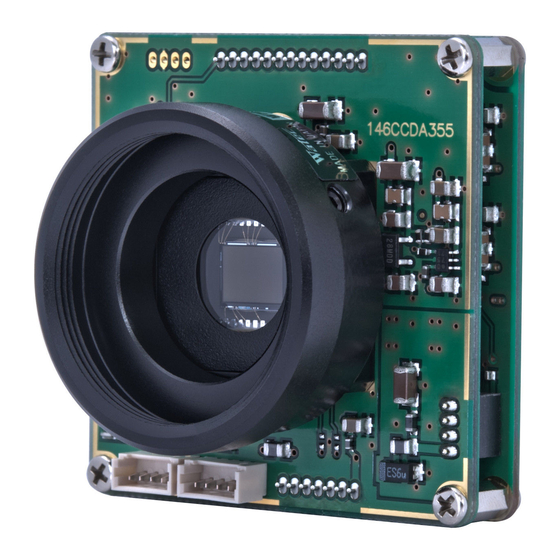
WAT-910BD H/W MANUAL 4. DESCRIPTION OF PARTS The name and function of each parts are as follows. When wiring, please be careful of the following pin arrangement and connect correctly. (Fig.4-1) Location of functional connectors (Fig.4-2) DC IRIS LENS adjustment VR... - Page 6 WAT-910BD H/W MANUAL (Fig.4-3) Connector Pin Function Parts Shape Name Parts No. Pin No. Description manufacturer ① power in(DC+12V) POWER BM02B-SRSS ① ② power GND(COMMON) ① VIDEO OUTPUT ① VIDEO OUT BM02B-SRSS ② VIDEO GND(COMMON) ① Sense- ② Sense+ DC IRIS CTL.
- Page 7 WAT-910BD H/W MANUAL (Fig.4-3) Connector Pin Function (continued) Parts Shape Name Parts No. Pin No. Description manufacturer ① GND(COMMON) ② SET ① OSD CTL. ③ LEFT (5key BM06B-GHS-TBT interface) ④ RIGHT ⑤ DOWN ⑥ UP - 4 -...
-
Page 8: Power Input
Absolute Maximum Ratings less than DC +16.0[V] Normally, We recommend to use WAT-910BD in "Supply Voltage Range(recommended) ". Using in range of "Supply Voltage Range(Capable)", the camera may be NOT damaged. In this case(especially lower voltage condition), please check followings. -
Page 9: Video Output
WAT-910BD H/W MANUAL 4.2 VIDEO OUTPUT An analog video output terminal of 75 ohm impedance. J2: VIDEO OUTPUT 75 ohm termination is needed in the video signal receiver equipment. (Fig.4-6) VIDEO output Parts Shape(Pin No.) Pin Name Description ① VIDEO OUTPUT 75 ohm impedance... -
Page 10: Dc Iris Lens Control
WAT-910BD H/W MANUAL 4.3 DC IRIS LENS CONTROL VR1: Adjustment VR(for DC IRIS LENS) This connector is used to connect a DC IRIS LENS. When connecting the lens, be careful to wire after confirming the pin assignments. J3: IRIS Connector(for DC IRIS LENS) -
Page 11: Video Iris Lens Control
WAT-910BD H/W MANUAL 4.4 VIDEO IRIS LENS CONTROL This connector is used to connect a VIDEO IRIS LENS. When connecting the lens, be careful to wire after confirming the pin assignments. J4: IRIS Connector(VIDEO DC IRIS LENS) (1) Wiring to the lens Pin assignments of JEITA recommended iris connector and J4 connector terminal have one-to-one correspondence as following. -
Page 12: Gpio(Motion Detect)
WAT-910BD H/W MANUAL 4.5 GPIO(MOTION DETECT) When using MOTION DETECTION function of WAT-910BD, it is possible to output the detection results from GPIO connector. For information about how to set up and use the motion detection feature, please refer to the OSD manual. -
Page 13: Osd Control
WAT-910BD H/W MANUAL 4.6 OSD CONTROL In order to operate the OSD, either a remote controller (RC-01) or electrical contacts(circuit) is required. The terminals of the J8 are pulled up with resistors inside of the camera. To move cursor and/or select a item on OSD, input the L pulse in each J8: OSD CTL.(5key interface) -
Page 14: Digital Video Out
WAT-910BD H/W MANUAL 5. DIGITAL VIDEO OUT Digital Video data can be output via the Digital Video Output Connector (J6) on the WAT-910BD. Use the OSD Menu or the SPI communication to switch the Digital Video Data Output ON/OFF. (1) Operation by OSD From the [SETUP] menu, select [FUNCTIONS], from the [FUNCTIONS] menu, switch the [DIGITAL OUT] feature between ON/OFF. -
Page 15: Electrical Characteristics
WAT-910BD H/W MANUAL 5.1 ELECTRICAL CHARACTERISTICS Each pin of the J6 Connector is connected directly to the Camera's DSP through a resistor. (3.3[V] CMOS level output. Does not go through buffer/driver.) The pinouts for each pin and a simplified circuit diagram are shown below. - Page 16 WAT-910BD H/W MANUAL The electrical characteristics for each pin are as described below. (Fig.5-5) Waveform and Sybols (DCK, DATA) (Fig.5-6) Electrical Characteristic Table (DCK, DATA) Parameter Symbol Unit Remarks Output High Voltage Ioh = 6mA Output Low Voltage Iol = -6mA...
-
Page 17: Digital Output Format
5.1 DIGITAL OUTPUT FORMAT (1)Video Data Format The WAT-910BD is a camera that conforms to the EIA/CCIR video format. The Analog Video Output (Video Output Connector:J2) is a composite video output which conforms to the EIA/CCIR standard, however, the digital video output does not fully comply with these standards. - Page 18 The effective image data is outputs the Luminance Data and Color Difference Data in Y/Cb/Cr=4:2:2 format. (The output sequence is repeated in the Cb,Y,Cr,Y,… sequence) Since the WAT-910BD is a monochrome camera, the Cb,Cr data are all 80[h]. The Horizontal Blanking Period (without TRC Code) is Cb,Cr=80[h], Y=10[h], repeated output.
- Page 19 WAT-910BD H/W MANUAL (1) EIA ODD Field(FLD1) V Blanking Timing H Blanking 22[Line] V Blanking D7-D0 OUT 515 516 517 518 519 520 521 522 523 524 525 (Line #) FLD2(EVEN FLD) FLD1(ODD FLD) ① ② ① EIA EVEN Field(FLD2) Active Video line...
- Page 20 WAT-910BD H/W MANUAL (2) EIA EVEN Field(FLD2) V Blanking Timing H Blanking 22[Line] V Blanking D7-D0 OUT 253 254 255 256 257 258 259 260 261 262 263 264 265 266 267 268 269 270 271 272 273 274 275 276 277 278...
- Page 21 WAT-910BD H/W MANUAL (3) CCIR ODD Field(FLD1) V Blanking Timing H Blanking 27[Line] V Blanking D7-D0 OUT 619 620 621 622 623 624 625 (Line #) FLD2(EVEN FLD) FLD1(ODD FLD) ⑤ ⑥ ⑤ CCIR EVEN Field(FLD2) Active Video line 1808[DCK/Line]...
- Page 22 WAT-910BD H/W MANUAL (4) CCIR EVEN Field(FLD1) V Blanking Timing H Blanking 26[Line] V Blanking D7-D0 OUT 307 308 309 310 311 312 313 314 315 316 317 318 319 320 321 322 323 324 325 326 327 328 329...
- Page 23 WAT-910BD H/W MANUAL (Fig.5-13) Digital Data Format(EIA) Line# EAV(4byte) H Blanking Data(300byte) SAV(4byte) V Blanking / Active Video Data(1512byte) → → V BLK ↓ ↓ ↓ (H Blanking Data) ↓ ↓ (V Blanking Data) → → → Y753 Y754 Y755...
- Page 24 WAT-910BD H/W MANUAL (Fig.5-14) Digital Data Format(CCIR) Line# EAV(4byte) H Blanking Data(330byte) SAV(4byte) V Blanking / Active Video Data(1478byte) → → V BLK ↓ ↓ ↓ (H Blanking Data) ↓ ↓ (V Blanking Data) → → → 80 Y736 80 Y737 80...
-
Page 25: Spi Communication
WAT-910BD H/W MANUAL 6. SPI COMMUNICATION By using the SPI communication connector (J7), various functions of WAT-910BD can be controlled directly, without using OSD. (1) SPI communication connector Refer to the following figure for the position of SPI communication connector (J7). -
Page 26: Electrical Characteristics
WAT-910BD H/W MANUAL 6.1 ELECTRICAL CHARACTERISTICS The pin arrangement and the outline circuit diagram of each pin are shown below. (Fig.6-2) Pin Function and Descriptions Parts Shape Name Parts No. Description manufacturer Pin No. ① SPI SLD (active L) ②... - Page 27 WAT-910BD H/W MANUAL (1) Preparation Though the communication specification of WAT-910BD applies to SPI bus specification fundamentally, it is implemented as 3 wire type. Connection of the communication port of external MCU (master) and a camera (slave) is made as follows.
- Page 28 WAT-910BD H/W MANUAL (Fig.6-5) N byte Write command (master to slave timing chart) (3) Command and Timing Chart(SPI Read Command) In the case of Read command, after sending the address of the needed data from external MCU to Camera DSP (master -> slave), it is outputted to external MCU from Camera DSP (slave -> master).
- Page 29 WAT-910BD H/W MANUAL (Fig.6-6) 1 byte Read command (master to slave and slave to master timing chart) (Fig.6-7) N byte Read command (master to slave and slave to master timing chart) - 26 -...
- Page 30 WAT-910BD H/W MANUAL (4) Actual wave form of "SPI Read Command" - 27 -...
-
Page 31: Ctl-Command Protocol
WAT-910BD H/W MANUAL 6.2 CTL-COMMAND PROTOCOL Camera CTL-COMMAND is executed by inside MCU on camera DSP. "CTL-COMMAND processing" is doing by "indirect parameter accessing". Camera MCU check the indirect registers to fetch CTL-COMMAND, and execute it immediately. Thus, to control camera and/or to read/write camera parameter, external MCU should send command, address, parameter value, check-sum and status CODE to indirect registers by using SPI write method. - Page 32 WAT-910BD H/W MANUAL Step.1: CTL-COMMAND SEND(EXT.MCU -> CAM DSP) CAMERA DSP Indirect Registors Address Symbol EXTERNAL 0x36 0x37 SPI Write 0x38 0x39 0x3A ST code 0x3B Set CTL-COMMAND to indirect registers from external MCU by SPI write command. Step.2: COMMAND LATCH and EXECUTION(CAM MCU)
- Page 33 WAT-910BD H/W MANUAL After command execution, camera MCU set execution results in indirect registers. For checking the end of CTL-COMMAN execution , external MCU should do SPI read and check data in ST(0x3B) register. If ST code is 55, it means "Command Execution Normally END" of CTL-COMMAND.
-
Page 34: Camera Ctl-Command
WAT-910BD H/W MANUAL 6.3 CAMERA CTL-COMMAND "Camera CTL-COMMAND" are shown in below. (1) CAMERA PARAMETER READ1(parameter address: 0x400 - 0x4FF) SPI Write "data set" Symbol Value *1: Parameter address lower byte. Assignable value range is 00 to FF. *2: Check sum (lower byte of "C1 + C2 + ADR + DAT") *In READ command, DAT value is always set 00. - Page 35 WAT-910BD H/W MANUAL (3) CAMERA PARAMETER WRITE1(address: 0x400 - 0x4FF) SPI Write "data set" Symbol Value *1: Parameter address lower byte. Assignable value range is 00 to FF. *2: Parameter Value. *3: Check sum (lower byte of "C1 + C2 + ADR + DAT") SPI Read "data set"(camera MCU response)
- Page 36 WAT-910BD H/W MANUAL (5) AREA DISPLAY ON/OFF SPI Write "data set" Symbol Value *1: WINDOW SELECT( BLC = 0x00, HSBLC = 0x01) *2: AREA DISPLAY ON: 0x01 / AREA DISPLAY OFF: 0x00 *3: Check sum (lower byte of "C1 + C2 + ADR + DAT") SPI Read "data set"(camera MCU response)
- Page 37 WAT-910BD H/W MANUAL (7) CAMERA PARAMETER SAVE SPI Write "data set" Symbol Value SPI Read "data set"(camera MCU response) Symbol Value *1: ST CODE(AA:in execution 55:EXEC.NORMALLY A5:EXEC.ERROR) *By executing this command, the parameter values t hat have been changed will be kept even after power on/off cycle.
-
Page 38: Camera Parameter
WAT-910BD H/W MANUAL 6.4 CAMERA PARAMETER Please do not change the bit or the byte data with the notation of "-" among following tables. (Camera operation will not be guaranteed.) The default value can be found in red underlined (or, with notation of default) in the table. - Page 39 WAT-910BD H/W MANUAL Address AGC MIN actual AGC MIN(dB) = ( [0x05 … 0xFF] * 4 * 0.035 ) + 5.3 (default:0x05, 約5.3(dB)) 0x414 (notice 1) Be sure to set 5 or more large values. (notice 2) Be sure to set small value less than all AGC LO/MID/HI MAX.
- Page 40 WAT-910BD H/W MANUAL Address 0x431 - - - - - - - - 0x432 - - - - - - - - 0x433 - - - - - - - - 0x434 - - - - - - - -...
- Page 41 WAT-910BD H/W MANUAL Address 0x454 - - - - - - - - 0x455 - - - - - - - - 0x456 - - - - - - - - 0x457 - - - - - - - -...
- Page 42 WAT-910BD H/W MANUAL Address MOTION AREA2 START H POSITION 0x46A 0x04:(LEFT) … 0x08 … 0xBB:(RIGHT) *Note that the sum of "H POSITION" and "H SIZE" is not to exceed 0xBF. MOTION AREA2 START V POSITION 0x46B 0x01:(TOP) … 0x28 … 0x8F:(BOTTOM) *Note that the sum of "V POSITION"...
- Page 43 WAT-910BD H/W MANUAL Address 0x47C - - - - - - - - 0x47D - - - - - - - - 0x47E - - - - - - - - 0x47F - - - - - - - -...
- Page 44 WAT-910BD H/W MANUAL Address ZOOM 0x4A8 - - - - - - - 0:OFF 1:ON ZOOM(magnification) 0x00:x1.0, 0x01:x1.1 … 0x09:x1.9, 0x0A:x2.0, 0x0B:x2.1 … 0x13:x2.9, 0x14:x3.0, 0x15:x3.1 … 0x1D:x3.9, 0x1E:x4.0, 0x1F:x4.5, 0x20:x5.0, 0x21:x5.5, 0x22:x6.0, 0x4A9 0x23:x6.5, 0x24:x7.0, 0x25:x7.5, 0x26:x8.0, 0x27:x9, 0x28:x10, 0x29:x11, 0x2A:x12,...
- Page 45 WAT-910BD H/W MANUAL Address 0x4C7 - - - - - - - - 0x4C8 - - - - - - - - 0x4C9 - - - - - - - - 0x4CA - - - - - - - -...
- Page 46 WAT-910BD H/W MANUAL Address SETUP(*1) SETUP LEVEL(*1) ON/OFF 0x4F3 - 0x00 … 0x1C … 0x0x3F 0:0(IRE) 1:7.5(IRE) 0x4F4 - - - - - - - - 0x4F5 - - - - - - - - 0x4F6 - - - -...
- Page 47 WAT-910BD H/W MANUAL Address 0x500 - - - - - - - - 0x501 - - - - - - - - 0x502 - - - - - - - - 0x503 - - - - - - - -...
- Page 48 WAT-910BD H/W MANUAL Address 0x52E - - - - - - - - 0x52F - - - - - - - - 0x530 - - - - - - - - 0x531 - - - - - - - -...
- Page 49 WAT-910BD H/W MANUAL Address 0x55C - - - - - - - - 0x55D - - - - - - - - 0x55E - - - - - - - - 0x55F - - - - - - - -...
- Page 50 WAT-910BD H/W MANUAL Address 0x58A - - - - - - - - 0x58B - - - - - - - - 0x58C - - - - - - - - 0x58D - - - - - - - -...
- Page 51 WAT-910BD H/W MANUAL Address 0x5B8 - - - - - - - - 0x5B9 - - - - - - - - 0x5BA - - - - - - - - 0x5BB - - - - - - - -...
- Page 52 WAT-910BD H/W MANUAL Address 0x5E0 - - - - - - - 0:(OFF) 1:START FACTORY RESET 0x5E1 - - - - - - - 0:OFF 1:ON DIGIT OUT 0x5E2 - - - - - - - 0:OFF 1:ON 0x5E3 -...
-
Page 53: Sample Code
WAT-910BD H/W MANUAL 6.5 SAMPLE CODE The following pages are example of the camera parameter change by SPI communication. In the examples, AGC mode is changed by using the method of 3WIRE SPI communication. (1)SAMPLE CODE This sample source code is installed in and tested on "R8C/1B" MCU made by Renesas. - Page 54 WAT-910BD H/W MANUAL // etc. void wait_ms(unsigned int) ; void wait_nop(void) ; // ---- main loop -------------------------------------------------------- void main(void) // loop counter // initialize MCU // inhibit interrupt(INT0) int0en = 0 ; prc0 = 1 ; hra00 = 1 ;...
- Page 55 WAT-910BD H/W MANUAL wait_ms(10) ; // 5ms waite SW_S_C[i+1] = p1 ; // read one more if (SW_S_C[i] == SW_S_C[i+1]){ i++ ; }else{ i = 0 ; // if SW status equal 3 times, check previous SW status. // if it is not equal, key input was changed and stable.
- Page 56 WAT-910BD H/W MANUAL break ; case 0x1B: // 5key LEFT RetV = BLC_AREA_OFF() ; break ; case 0x17: // 5key RIGHT RetV = BLC_AREA_ON() ; break ; case 0x0F: // 5key SET // AGC MODE change RetV = AGC_MODE() ;...
- Page 57 WAT-910BD H/W MANUAL SEND_BUFF[7] = 0xAA ; return SPI_WRITE_3W(0x36, 8) ; unsigned char BLC_AREA_ON(void) SEND_BUFF[2] = 0x01 ; SEND_BUFF[3] = 0x00 ; SEND_BUFF[4] = 0x00 ; SEND_BUFF[5] = 0x01 ; // BLC AREA ON SEND_BUFF[6] = 0x02 ; SEND_BUFF[7] = 0xAA ;...
- Page 58 WAT-910BD H/W MANUAL //---------------------------------------------------------------------- // FUNCTION: SPI_WRITE_3W // SPI WRITE SEND_BUFF[0...(W_Byte-1)] // In case of Indirect access, it must W_Adr = 0x36 and W_Byte = 8. // In case of 3Wire, it need change GPIO(MISO/MOSI) direction // input/output. //---------------------------------------------------------------------- unsigned char SPI_WRITE_3W(unsigned char W_Adr, unsigned char W_Byte) int i ;...
- Page 59 WAT-910BD H/W MANUAL SPI_READ_3W(0x3B, 1) ; // ST CODE read wait_ms(1) ; // 1mS wait if( READ_BUFF[0] == 0x55){ // 0x55 means EXEC.NORMALLY return TRUE ; }else{ return FALSE ; //---------------------------------------------------------------------- // FUNCTION: SPI_READ_3W // SPI WRITE READ_BUFF[0...(R_Byte-1)] // In case of 3Wire, it need change GPIO(MISO/MOSI) direction // input/output.
- Page 60 WAT-910BD H/W MANUAL i ++ ; // next byte wait_nop() ; // SPI READ start pd3_3 = 0 ; // set port direction MISO(input) wait_nop() ; wait_nop() ; wait_nop() ; wait_nop() ; i = 0 ; while( i < R_Byte ){ // Loop R_Byte times j = 0 ;...
- Page 61 WAT-910BD H/W MANUAL (2)SAMPLE WAVEFORM e.g. Change AGC MODE ( MID -> HI ) by using SPI(3wire) communucation. Step *1: Send "CAMERA PARAMETER READ1 command" to indirect registers(CAMERA: Address 0x36 - 0x3B) to get "AGC MODE: Address=0x401" parameter from CAMERA.
- Page 62 WAT-910BD H/W MANUAL → SCLK → MOSI/MIS0 → ← Retry and get ST CODE = EXEC.NORMALLY. Step *3: By using "SPI read command", get "AGC MODE: Address=0x401" parameter value from CAMERA. → SCLK → MOSI/MIS0 → (LSB first) 1000 1110 0000...
- Page 63 WAT-910BD H/W MANUAL Step *5: Send "SPI read command" to get and check ST CODE(address:0x3B). → SCLK → MOSI/MIS0 → (LSB first) 1110 1110 0000 0000 1010 1010 (MSB first) MOSI DATA MISO DATA EXEC.NORMALLY - 60 -...
-
Page 64: Specifications
WAT-910BD H/W MANUAL 7. SPECIFICATIONS WAT-910BD (EIA) WAT-910BD (CCIR) Model 1/2 inch interline transfer CCD image sensor Pick-up element Number of total pixels 811 (H) × 508 (V) 795 (H) × 596 (V) 768 (H) × 494 (V) 752 (H) × 582 (V) -
Page 65: Dimensions
WAT-910BD H/W MANUAL 8. DIMENSIONS Unit:(mm) - 62 -...
Need help?
Do you have a question about the WAT-910BD and is the answer not in the manual?
Questions and answers