Table of Contents
Advertisement
QQ
3 7 63 1515 0
SERVICE MANUAL
Ver 1.0 2003.02
System
TE
L 13942296513
Compact disc digital audio system
Laser diode properties
Material: GaAlAs
Wavelength: λ = 780 nm
Emission duration: Continuous
Laser output: Less than 44.6 µW (This output is the value measured at a
distance of 200 mm from the objective lens surface on the optical pick-up
block with 7 mm aperture.)
D-FJ210 :
Frequency range (10k/9k switch)
10 kHz step:
TV: 2 - 13 ch
WB (weather band): 1 - 7 ch
FM: 87.5 - 108.0 MHz
AM: 530 - 1710 kHz
9 kHz step:
TV: 2 - 13 ch
WB (weather band): 1 - 7 ch
FM: 87.5 - 108.0 MHz
AM: 531 - 1710 kHz
D-FJ215 :
Frequency range (Chinese model)
FM: 87.5 - 108.0 MHz
AM: 531 - 1602 kHz
Frequency range (10k/9k switch) (except Chinese model)
• 9 kHz step:
FM: 87.5 - 108.0 MHz
AM: 531 - 1 602 kHz
• 10 kHz step:
www
FM: 87.5 - 108.0 MHz
AM: 530 - 1 710 kHz
.
Sony Corporation
9-877-064-01
2003B0200-1
Personal Audio Company
© 2003.02
Pubulished by Sony Engineering Corporation
http://www.xiaoyu163.com
D-FJ210/FJ215
SPECIFICATIONS
TV/WB/FM/AM PORTABLE CD PLAYER
x
ao
y
i
http://www.xiaoyu163.com
8
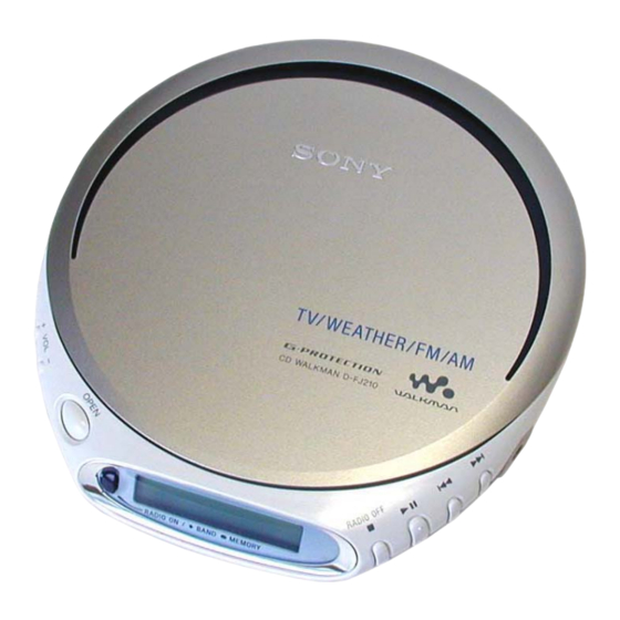
Photo : D-FJ210
Model Name Using Similar Mechanism D-EJ360
CD Mechanism Type
Optical Pick-up Type
Q Q
Power requirements
3
6 7
1 3
For the area code of the model you purchased, check the upper left side of
the bar code on the package.
• Two Sony NH-7WMAA rechargeable batteries: 1.2 V DC x 2
• Sony NH-WM2AA rechargeable batteries: 1.2 V DC x 2
• Two LR6 (size AA) batteries: 1.5 V x 2 DC
• AC power adaptor (DC IN 4.5 V jack):
US model: 120 V, 60 Hz
E13 model: 220 - 230 V, 50/60 Hz
Australian model: 240 V, 50 Hz
Hong Kong model: 230 V, 50 Hz
Chinese model: 220 V, 50 Hz
Dimensions (w/h/d) (without projecting parts and controls)
Approx. 136 x 26 x 150 mm (5
Mass (excluding accessories)
Approx. 205 g (7.3 oz)
Operating temperature
5°C - 35°C (41°F - 95°F)
Design and specifications are subject to change without notice.
FJ-210 :
Headphones/earphones with the remote control (1)
FM/AM PORTABLE CD PLAYER
u163
.
2 9
9 4
2 8
Australian Model
Chinese Model
1 5
0 5
8
2 9
9 4
3
⁄
x 1
1
⁄
x 6 in.)
8
16
Supplied Accessories
m
co
9 9
US Model
D-FJ210
E Model
D-FJ215
CDM-3325ER
DAX-25E
2 8
9 9
D-FJ210
D-FJ215
Advertisement
Table of Contents

Related Manuals for Sony D-FJ210


Summary of Contents for Sony D-FJ210
-
Page 1: Specifications
For the area code of the model you purchased, check the upper left side of the bar code on the package. Laser diode properties • Two Sony NH-7WMAA rechargeable batteries: 1.2 V DC x 2 Material: GaAlAs • Sony NH-WM2AA rechargeable batteries: 1.2 V DC x 2 Wavelength: λ... -
Page 2: Table Of Contents
PARTS LIST ARE CRITICAL TO SAFE OPERATION. (Caution: Some printed circuit boards may not come printed REPLACE THESE COMPONENTS WITH SONY PARTS WHOSE with the lead free mark due to their particular size.) PART NUMBERS APPEAR AS SHOWN IN THIS MANUAL OR IN SUPPLEMENTS PUBLISHED BY SONY. -
Page 3: Servicing Notes
CD player (front) Strap holes DC IN 4.5 V (external power OPEN input) jack . > i (headphones) jack • RADIO OFF (D-FJ210) x / CHG • RADIO OFF (D-FJ215) SOUN/AVLS Display P MODE/ F RADIO ON/BAND • MEMORY VOL +*/– HOLD *The button has a tactile dot. -
Page 4: Disassembly
D-FJ210/FJ215 SECTION 3 3 7 63 1515 0 DISASSEMBLY The equipment can be removed using the following procedure. MD ASSY “Motor ASSY (Sled) (M902)”, Optical pick-up (DAX-25E), Upper lid ASSY, “Motor ASSY, turn table (spindle) (M901)” Cabinet (upper) sub ASSY Main board Note : Follow the disassembly procedure in the numerical order given. -
Page 5: Md Assy, Main Board
D-FJ210/FJ215 3 7 63 1515 0 3-2. MD ASSY, MAIN BOARD 5 MD ASSY 1 CN601 2 Connector (CN401) 7 MAIN board 3 Connector (CN402) Cabinet (lower) sub ASSY L 13942296513 3-3. “MOTOR ASSY (SLED) (M902)”, OPTICAL PICK-UP (DAX-25E), “MOTOR ASSY, TURN TABLE (SPINDLE) (M901)”... -
Page 6: Electrical Adjustmens
D-FJ210/FJ215 SECTION 4 3 7 63 1515 0 ELECTRICAL ADJUSTMENTS • Repeat the procedures in each adjustment several times, and the TUNER SECTION 0 dB = 1µV frequency coverage and tracking adjustments should be finally AM section done by the trimmer capacitors. - Page 7 D-FJ210/FJ215 3 7 63 1515 0 Adjustment Location : Main board Frequency Coverage Adjustment Setting : digital voltmeter [MAIN BOARD] (DC range) (Side A) TJ1 (VT) TJ6 (TU GND) TJ304 J102 D306 C810 TAP1 VDR305 VDR302 (FM RF IN)
- Page 8 D-FJ210/FJ215 3 7 63 1515 0 RF Level Check CD SECTION Condition: The CD section adjustments are done automatically in this set. • Hold the set in horizontal state. Precautions for Check Connection: 1. Perform check in the order given.
-
Page 9: Diagrams
D-FJ210/FJ215 SECTION 5 DIAGRAMS 3 7 6 3 1 5 1 5 0 5-1. BLOCK DIAGRAM –CD SECTION– FJ210 FJ215 IC602 IC603 D-RAM(16M) D-RAM(4M) D0-3 A0-10 D0-3 A0-9 2,3,24,25 9-12,15-19,21,8 5 23 4 2,3,24,25 9-12,14-18,5 4 23 3 IC301... -
Page 10: Block Diagram -Tuner Section
D-FJ210/FJ215 3 7 6 3 1 5 1 5 0 5-2. BLOCK DIAGRAM –TUNER SECTION– TV/FM/AM FRONTEND, FM MPX FJ210 TV-RF TU_L SECTION FM-IF_I DET_O MPX_I FM/TV FM-MIX_O (Page 9) SECTION FM-RF TU_R (Page 9) FJ210 FM-IF TV-RF_O LPF2A... -
Page 11: Printed Wiring Boards (Fj215 Only) -Side A
D-FJ210/FJ215 3 7 6 3 1 5 1 5 0 5-3. PRINTED WIRING BOARDS –SIDE A– (FJ215 ONLY) • Refer to page 19 for Notes. : USES UNLEADED SOLDER. S802 S801 TJ202 S804 TJ304 TJ102 TJ304 MAIN BOARD TJ303... -
Page 12: Printed Wiring Boards (Fj215 Only) -Side B
D-FJ210/FJ215 3 7 6 3 1 5 1 5 0 PRINTED WIRING BOARDS –SIDE B– (FJ215 ONLY) • Refer to page 19 for Notes. : USES UNLEADED SOLDER. MAIN BOARD C323 (SIDE B) VDR303 D-FJ215 R308 C630 TP15 TP620... -
Page 13: Printed Wiring Boards (Fj210 Only) -Side A
D-FJ210/FJ215 3 7 6 3 1 5 1 5 0 5-4. PRINTED WIRING BOARDS –SIDE A– (FJ210 ONLY) • Refer to page 19 for Notes. : USES UNLEADED SOLDER. S802 S801 TJ202 S804 TJ304 TJ304 TJ102 MAIN BOARD TJ303... -
Page 14: Printed Wiring Boards (Fj210 Only) -Side B
D-FJ210/FJ215 3 7 6 3 1 5 1 5 0 PRINTED WIRING BOARDS –SIDE B– (FJ210 ONLY) • Refer to page 19 for Notes. : USES UNLEADED SOLDER. MAIN BOARD C323 (SIDE B) VDR303 (FJ210) R308 C630 TP15 TP620... -
Page 15: Schematic Diagram -Main Section (1/4)
D-FJ210/FJ215 3 7 6 3 1 5 1 5 0 5-5. SCHEMATIC DIAGRAM – MAIN SECTION (1/4) – • Refer to page 19 for Notes. 1 3 9 4 2 2 9 6 5 1 3 w w w u 1 6 3 http://www.xiaoyu163.com... -
Page 16: Schematic Diagram -Main Section (2/4)
D-FJ210/FJ215 3 7 6 3 1 5 1 5 0 5-6. SCHEMATIC DIAGRAM – MAIN SECTION (2/4) – • Refer to page 19 for Notes. 1 3 9 4 2 2 9 6 5 1 3 w w w u 1 6 3 http://www.xiaoyu163.com... -
Page 17: Schematic Diagram -Main Section (3/4)
D-FJ210/FJ215 3 7 6 3 1 5 1 5 0 5-7. SCHEMATIC DIAGRAM – MAIN SECTION (3/4) – • Refer to page 19 for Notes. • Refer to page 22 for IC Pin Function Description. 1 3 9 4 2 2 9 6 5 1 3... -
Page 18: Schematic Diagram -Main Section (4/4)
D-FJ210/FJ215 3 7 6 3 1 5 1 5 0 5-8. SCHEMATIC DIAGRAM – MAIN SECTION (4/4) – • Refer to page 19 for Notes. 1 3 9 4 2 2 9 6 5 1 3 w w w u 1 6 3 http://www.xiaoyu163.com... -
Page 19: Caution
D-FJ210/FJ215 3 7 63 1515 0 Note on schematic diagrams. Note on Printed Wiring Boards: • X : parts extracted from the component side. • All capacitors are in µF unless otherwise noted. pF: µµF 50 WV or •... - Page 20 D-FJ210/FJ215 3 7 63 1515 0 • IC BLOCK DIAGRAM TA2154FN (EL) BUFF FM/AM/TV PW SW 1/8 OR BUFF 1/16 IF BUFF LEVEL BUFF TV RF FM IF AM IF FM/TV FM MPX FM RF IC601 BU9354KV L 13942296513...
- Page 21 D-FJ210/FJ215 3 7 63 1515 0 IC403 BH6580KV 59 58 57 56 55 H BRIDGE H BRIDGE H BRIDGE 40 LATCH DCIN HVPROT 39 DATA REGB LEVEL CONTROLLER SHIFTER 38 CLOXK 37 WAKEUP DCIN_S XRST CHGB CHARGE VMMNT RESET_O...
-
Page 22: Ic Pin Function Description
D-FJ210/FJ215 3 7 63 1515 0 5-9. IC PIN FUNCTION DESCRINTION IC801 (SYSTEM CONTROL) T5AW6-Z7C Pin No. Pin name Description – Ground terminal System clock input XOUT Not used (OPEN) TEST Test mode terminal VCPU_2.0V – Power supply for CPU & I/O... - Page 23 D-FJ210/FJ215 3 7 63 1515 0 Pin No. Pin name Description PGM_SDTI – Not used (OPEN) PGM_SCK_O – Not used (OPEN) CD_ON CD ON signal output GFS_I Guard Frame Synchronous signal input FG_I FG signal input PGMSEL_O – Not used (OPEN)
-
Page 24: Exploded Views
D-FJ210/FJ215 SECTION 6 3 7 63 1515 0 EXPLODED VIEWS NOTE : • Hardware (# mark) list and accessories and • -XX, -X mean standardized parts, so they packing materials are given in the last of this The components identified by mark 0 may have some difference from the original parts list. -
Page 25: Optical Pick-Up Section (Cdm-3325Er)
D-FJ210/FJ215 3 7 63 1515 0 6-2. OPTICAL PICK-UP SECTION (CDM-3325ER) M902 M901 L 13942296513 The components identified by mark 0 or dotted line with mark 0 are critical for safety. Replace only with part number specified. Ref. No. -
Page 26: Electrical Parts List
D-FJ210/FJ215 SECTION 7 MAIN ELECTRICAL PARTS LIST 3 7 63 1515 0 NOTE : • Due to standardization, replacements in the • SEMICONDUCTORS The components identified by mark 0 parts list may be different from the parts In each case, u : µ , for example :... - Page 27 D-FJ210/FJ215 MAIN 3 7 63 1515 0 Ref. No. Part No. Description Remark Ref. No. Part No. Description Remark 1-162-915-11 CERAMIC CHIP 10PF 0.5PF C318 1-115-467-11 CERAMIC CHIP 0.22uF 1-117-863-11 CERAMIC CHIP 0.47uF 6.3V C319 1-162-968-11 CERAMIC CHIP 0.0047uF 10% 1-107-826-11 CERAMIC CHIP 0.1uF...
- Page 28 D-FJ210/FJ215 MAIN 3 7 63 1515 0 Ref. No. Part No. Description Remark Ref. No. Part No. Description Remark C612 1-162-970-11 CERAMIC CHIP 0.01uF D302 8-719-044-74 DIODE MA792WK-TX (FJ210) C613 1-162-970-11 CERAMIC CHIP 0.01uF D306 8-719-059-53 DIODE MA3J14700LSO C614 1-162-966-11 CERAMIC CHIP 0.0022uF 10%...
- Page 29 D-FJ210/FJ215 MAIN 3 7 63 1515 0 Ref. No. Part No. Description Remark Ref. No. Part No. Description Remark 1-414-398-11 INDUCTOR 10uH 1-216-853-11 METAL CHIP 470K 1/10W 1-412-006-31 INDUCTOR 10uH 1-216-833-11 METAL CHIP 1/10W 1-412-006-31 INDUCTOR 10uH 1-216-864-11 METAL CHIP...
- Page 30 D-FJ210/FJ215 MAIN 3 7 63 1515 0 Ref. No. Part No. Description Remark Ref. No. Part No. Description Remark 1-216-864-11 METAL CHIP 1/10W R414 1-216-864-11 METAL CHIP 1/10W 1-218-871-11 METAL CHIP 0.5% 1/10W R416 1-216-813-11 METAL CHIP 1/10W 1-218-871-11 METAL CHIP 0.5%...
- Page 31 D-FJ210/FJ215 MAIN 3 7 63 1515 0 Ref. No. Part No. Description Remark Ref. No. Part No. Description Remark R801 1-216-295-91 SHORT CHIP S806 1-786-211-21 SWITCH, KEYBOARD (x,RADIO OFF) R802 1-216-864-11 METAL CHIP 1/10W S807 1-786-211-21 SWITCH, KEYBOARD (.,PRESET/TUNE -)
- Page 32 D-FJ210/FJ215 3 7 63 1515 0 REVISION HISTORY Clicking the version allows you to jump to the revised page. Also, clicking the version at the upper right on the revised page allows you to jump to the next revised page.
Need help?
Do you have a question about the D-FJ210 and is the answer not in the manual?
Questions and answers