Sony D-FJ200 Service Manual
Fm/am portable cd player
Hide thumbs
Also See for D-FJ200:
- Service manual (34 pages) ,
- Operating instructions (2 pages) ,
- Specifications (2 pages)
Table of Contents
Advertisement
Quick Links
SERVICE MANUAL
Ver. 1.3 2005.12
System
Compact disc digital audio system
Laser diode properties
Material: GaAlAs
Wavelength: λ = 780 nm
Emission duration: Continuous
Laser output: Less than 44.6 µW (This output is the value
measured at a distance of 200 mm from the objective lens
surface on the optical pick-up block with 7 mm aperture.)
Frequency range (AEP, UK, CH, E13 models)
FM: 87.5 - 108.0 MHz
AM: 531 - 1 602 kHz
Frequency range (10k/9k)
• D-FJ200:US/FJ201
9 kHz step:
TV: 2 - 13 ch (US)
WB (Weather band): 1 - 7 ch (US)
FM: 87.5 - 108.0 MHz
AM: 531 - 1 710 kHz
10 kHz step:
TV: 2 - 13 ch (US)
WB (Weather band): 1 - 7 ch (US)
FM: 87.5 - 108.0 MHz
AM: 530 - 1 710 kHz
Sony Corporation
9-961-978-04
2005L02-1
Parsonal Audio Division
Published by Sony Engineering Corporation
© 2005.12
D-FJ200/FJ201
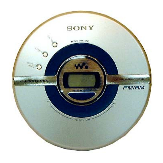
Photo : D-FJ200
SPECIFICATIONS
• Australian model
9 kHz step:
FM: 87.5 - 108.0 MHz
AM: 531 - 1 602 kHz
10 kHz step:
FM: 87.5 - 108.0 MHz
AM: 530 - 1 710 kHz
Power requirements
• Two Sony NH-7WMAA rechargeable batteries:
1.2 V DC x 2
• Two LR6 (size AA) batteries: 1.5 V DC x 2
• AC power adaptor (DC IN 4.5 V jack):
220 V, 50 Hz (Chinese)
120 V, 60 Hz (D-FJ201)
220-230V, 50/60 Hz (AEP, UK, EE, E13,HK)
240 V, 50Hz (Australian)
Dimensions (w/h/d) (without projecting parts and controls)
Approx. 135.8 x 24.3 x 135.8 mm (5
Mass (excluding accessories)
Approx. 191 g (6.8 oz.)
Operating temperature
5°C - 35°C (41°F - 95°F)
Design and specifications are subject to change without notice.
Australian Model
Chinese Model
Model Name Using Similar Mechanism New
CD Mechanism Type
Optical Pick-up Type
FM/AM PORTABLE CD PLAYER
US Model
AEP Model
UK Model
D-FJ200
E Model
D-FJ200/FJ201
CDM-3325ER
DAX-25E
3
1
3
⁄
x 3
⁄
x 5
⁄
in.)
8
32
8
Advertisement
Table of Contents

Related Manuals for Sony D-FJ200


Summary of Contents for Sony D-FJ200
-
Page 1: Specifications
200 mm from the objective lens Power requirements surface on the optical pick-up block with 7 mm aperture.) • Two Sony NH-7WMAA rechargeable batteries: 1.2 V DC x 2 Frequency range (AEP, UK, CH, E13 models) •... -
Page 2: Table Of Contents
MARK 0 ON THE SCHEMATIC DIAGRAMS AND IN THE PARTS the lead free mark due to their particular size.) LIST ARE CRITICAL TO SAFE OPERATION. REPLACE THESE COMPONENTS WITH SONY PARTS WHOSE PART NUMBERS APPEAR AS SHOWN IN THIS MANUAL OR IN SUPPLEMENTS : LEAD FREE MARK PUBLISHED BY SONY. -
Page 3: Servicing Notes
D-FJ200/FJ201 SECTION 1 SERVICING NOTES Laser Diode Checking Methods NOTES ON HANDLING THE OPTICAL PICK-UP BLOCK OR During normal operation of the equipment, emission of the laser diode BASE UNIT is prohibited unless the upper panel is closed while turning ON the S809(push switch type). -
Page 4: Disassembly
D-FJ200/FJ201 SECTION 3 DISASSEMBLY The equipment can be removed using the following procedure. Upper lid ASSY, Cabinet (upper) ASSY MD ASSY Motor ASSY (Sled) (M902), Optical pick-up (DAX-25E), Turn table motor ASSY (spindle) (M901) Cabinet (lower) ASSY Main board Note : Follow the disassembly procedure in the numerical order given. -
Page 5: Md Assy (Cdm-3325Er), Main Board
D-FJ200/FJ201 3-2. MD ASSY (CDM-3325ER), MAIN BOARD 5 MD assy (CDM-3325ER) 1 CN601 2 CN402 3 CN402 7 MAIN board HOW TO SET THE HARNESS IN ASSEMBLING CN401 CN402 harness... -
Page 6: Motor Assy (Sled) (M902), Optical Pick-Up (Dax-25E), Turn Table Motor Assy(Spindle) (M901)
D-FJ200/FJ201 3-3. MOTOR ASSY (SLED) (M902), OPTICAL PICK-UP (DAX-25E), TURN TABLE MOTOR ASSY (SPINDLE) (M901) 1 three screws (B1.7x4) 3 gear cover 8 three screws (B1.7x4) 5 motor assy (sled) (M902) 7 optical pick-up (DAX-25E) q; turn table motor assy... -
Page 7: Electrical Adjustments
D-FJ200/FJ201 SECTION 4 ELECTRICAL ADJUSTMENTS • Repeat the procedures in each adjustment several times, and the Adjustment Location : 0 dB = 1µV TUNER SECTION frequency coverage and tracking adjustments should be finally [MAIN BOARD] (SIDE B) CT1 : AM Tracking Adjustment AM section done by the trimmer capacitors. -
Page 8: Diagrams
D-FJ200/FJ201 SECTION 5 Ver. 1.3 DIAGRAMS 5-1. BLOCK DIAGRAM –CD SECTION– IC602 D-RAM(16M) D0-3 A0-10 2,3,24,25 9-12,15-19,21,8 5 23 4 IC301 PRE EQ AMP/EVR/ HADPHONE AMP IC601 TUNER TUNER TU_L VCC2 RF AMP,SERVO SECTION SECTION DIGITAL SIGNAL PROCESSOR TU_R OPTICAL... -
Page 9: Block Diagram -Tuner Section
D-FJ200/FJ201 Ver. 1.3 5-2. BLOCK DIAGRAM –TUNER SECTION– D-FJ200: US/FJ201 TV/FM/AM FRONTEND, FM MPX TV-RF TU_L SECTION FM-IF_I DET_O MPX_I FM/TV FM-MIX_O (Page 8) SECTION FM-RF TU_R (Page 8) FM-IF EXCEPT US FJ200:US TV-RF_O LPF2A TV/WB TU-VCC (TV RF) LPF2B... -
Page 10: Printed Wiring Boards -Main Section (Side A)
D-FJ200/FJ201 Ver. 1.3 5-3. PRINTED WIRING BOARDS – MAIN SECTION (SIDE A) – : Uses unleaded solder. FERRITE-BAR ANTENNA • Semiconductor C624 MAIN BOARD (SIDE A) R446 Location C7 C2 Ref. No. Location R612 X601 C633 D306 C630 R616 D400... -
Page 11: Printed Wiring Boards -Main Section (Side B)
D-FJ200/FJ201 Ver. 1.3 PRINTED WIRING BOARDS – MAIN SECTION (SIDE B) – : Uses unleaded solder. OPTICAL PICK-UP BLOCK DAX-25E • Semiconductor Location MAIN BOARD (SIDE B) Ref. No. Location IC602 D301 EXCEPT AEP,UK,EE D302 D403 C311 D408 D804 R314... -
Page 12: Schematic Diagram -Main Section (1/5)
D-FJ200/FJ201 Ver 1.2 5-4. SCHEMATIC DIAGRAM – MAIN SECTION (1/5) –... -
Page 13: Schematic Diagram -Main Section (2/5)
D-FJ200/FJ201 Ver. 1.3 5-5. SCHEMATIC DIAGRAM – MAIN SECTION (2/5) – EXCEPT AEP,UK,EE EXCEPT AEP,UK,EE EXCEPT AEP,UK,EE EXCEPT AEP,UK,EE EXCEPT AEP,UK,EE... -
Page 14: Schematic Diagram -Main Section (3/5)
D-FJ200/FJ201 Ver. 1.3 5-6. SCHEMATIC DIAGRAM – MAIN SECTION (3/5) – • See page 22 for IC Pin Function Description. EXCEPT AEP,UK,EE... -
Page 15: Schematic Diagram -Main Section (4/5)
D-FJ200/FJ201 Ver. 1.3 5-7. SCHEMATIC DIAGRAM – MAIN SECTION (4/5) – US,AEP,UK,EE,C&SA US,AEP,UK,EE,C&SA... -
Page 16: Schematic Diagram -Main Section (5/5)
D-FJ200/FJ201 Ver. 1.3 5-8. SCHEMATIC DIAGRAM – MAIN SECTION (5/5) – • See page 20 for IC Pin Function Description. - Page 17 D-FJ200/FJ201 Ver 1.2 For Schematic Diagrams. For Printed Wiring Boards: Note: Note: • All capacitors are in µF unless otherwise noted. pF: µµF 50 WV or • X : parts extracted from the component side. • : internal component. less are not indicated except for electrolytics and tantalums.
-
Page 18: Ic Block Diagram
D-FJ200/FJ201 • IC BLOCK DIAGRAM TA2154FN (EL) BUFF FM/AM/TV PW SW 1/8 OR BUFF 1/16 IF BUFF LEVEL BUFF TV RF FM IF AM IF FM/TV FM MPX FM RF IC601 BU9354CKV 99 98 97 96 95 94 93 92 91 90 88 87 86 85 84 83 82 81 80 79 78 77 76 AVDD1_2.0V... - Page 19 D-FJ200/FJ201 IC403 BH6580KV 59 58 57 56 55 H BRIDGE H BRIDGE H BRIDGE 40 POWER_LT_I DCIN HVPROT 39 XSDTO REGB LEVEL CONTROLLER SHIFTER 38 XSCK 37 WAKEUP_I DCIN_S XRST_I CHGB CHARGE VMMNT H_RESET SYNC CHGMNT PRE_GND BATM1 SOFT 10msec...
-
Page 20: Ic Pin Function Description
D-FJ200/FJ201 5-9. IC PIN FUNCTION DESCRINTION IC3 (DIGITAL TUNING, LCD DRIVER CONTROL TC9327AF-04CD) Pin No. Pin name Description 1 to 4 COM1 to 4 LCD common output 5 to 20 S1 to 16 LCD segment output AM-STEP_I Tuning frequency (9k/10k) step select signal input... - Page 21 D-FJ200/FJ201 Pin No. Pin name Description HOLD_I Not used (Fixed to L) NC (OT1) Not used (OPEN) – Ground NC (FM_I) Not used (OPEN) TV/FM/AM_I Tuner OSC frequency input VDD (1.8-2.2V) – Power supply RESET_I Reset signal input Crystal oscillator output (75kHz) Crystal oscillator input (75kHz) –...
- Page 22 D-FJ200/FJ201 IC801 (SYSTEM CONTROL) T5AW5-04CD Pin No. Pin name Description – Ground terminal System clock input Not used (OPEN) TEST Test mode terminal VCPU_2.0V – Power supply FOK_I Focus OK signal input XBUSY_I Auto sequencer status signal input from IC601...
- Page 23 D-FJ200/FJ201 Pin No. Pin name Description PGM_SDTI_I PGM serial data input PGM_SCK_O PGM clock output CD_ON_O CD ON signal output to IC3 GFS_I Guard Frame Synchronous signal input from IC601 FG_I FG signal input from IC403 PGM/SC_SEL_O PGM select signal output...
-
Page 24: Exploded Views
D-FJ200/FJ201 Ver. 1.3 SECTION 6 EXPLODED VIEWS NOTE : The components identified by • -XX, -X mean standardized parts, so they may • The mechanical parts with no reference number mark 0 or dotted line with mark have some difference from the original one. -
Page 25: Cabinet Section
D-FJ200/FJ201 Ver. 1.3 6-2. CABINET SECTION CDM-3325ER Ref. No. Part No. Description Remark Ref. No. Part No. Description Remark 3-261-238-01 KNOB (HOLD) 3-261-240-02 LEVER (DETECTION) 3-261-305-01 CABINET (LOWER) 3-261-239-01 KNOB (OPEN) A-4541-837-A MAIN BOARD, COMPLETE (FJ200:US) 3-254-070-11 SCREW A-4542-741-A MAIN BOARD, COMPLETE (FJ200:AEP,UK,EE) A-4542-745-A MAIN BOARD, COMPLETE (FJ201:C&SA) -
Page 26: Optical Pick-Up Section (Cdm-3325Er)
D-FJ200/FJ201 6-3. OPTICAL PICK-UP SECTION (CDM-3325ER) M902 M901 The components identified by mark 0 or dotted line with mark 0 are critical for safety. Replace only with part number specified. Ref. No. Part No. Description Remark Ref. No. Part No. -
Page 27: Electrical Parts List
D-FJ200/FJ201 Ver. 1.3 SECTION 7 MAIN ELECTRICAL PARTS LIST NOTE: The components identified by • Due to standardization, replacements in the • RESISTORS mark 0 or dotted line with mark parts list may be different from the parts All resistors are in ohms. - Page 28 D-FJ200/FJ201 Ver. 1.3 MAIN Ref. No. Part No. Description Remarks Ref. No. Part No. Description Remarks 1-107-826-11 CERAMIC CHIP 0.1uF C325 1-162-970-11 CERAMIC CHIP 0.01uF 1-162-919-11 CERAMIC CHIP 22PF C330 1-216-864-11 METAL CHIP 1/10W 1-162-910-11 CERAMIC CHIP 0.25PF 50V C400 1-117-720-11 CERAMIC CHIP 4.7uF...
- Page 29 D-FJ200/FJ201 Ver. 1.3 MAIN Ref. No. Part No. Description Remarks Ref. No. Part No. Description Remarks C631 1-164-156-11 CERAMIC CHIP 0.1uF 1-216-864-11 METAL CHIP 1/10W C632 1-107-826-11 CERAMIC CHIP 0.1uF (EXCEPT US) C633 1-164-156-11 CERAMIC CHIP 0.1uF 1-414-760-21 FERRITE (FJ200:US)
- Page 30 D-FJ200/FJ201 Ver. 1.3 MAIN Ref. No. Part No. Description Remarks Ref. No. Part No. Description Remarks 1-412-006-31 INDUCTOR 10uH 1-216-821-11 METAL CHIP 1/10W L301 1-400-389-21 INDUCTOR 10uH 1-216-829-11 METAL CHIP 4.7K 1/10W L302 1-400-681-21 INDUCTOR 0uH (FJ200:US) (FJ200:US/FJ201:C&SA) 1-216-864-11 METAL CHIP...
- Page 31 D-FJ200/FJ201 Ver. 1.3 MAIN Ref. No. Part No. Description Remarks Ref. No. Part No. Description Remarks 1-218-903-11 METAL CHIP 220K 0.5% 1/10W R203 1-216-829-11 METAL CHIP 4.7K 1/10W (EXCEPT AEP,UK,EE) (EXCEPT AEP,UK,EE) R204 1-216-829-11 METAL CHIP 4.7K 1/10W 1-218-855-11 METAL CHIP 2.2K...
- Page 32 D-FJ200/FJ201 Ver. 1.3 MAIN Ref. No. Part No. Description Remarks Ref. No. Part No. Description Remarks R608 1-216-789-11 METAL CHIP 1/10W R862 1-216-837-11 METAL CHIP 1/10W R609 1-216-845-11 METAL CHIP 100K 1/10W R863 1-216-821-11 METAL CHIP 1/10W R610 1-216-845-11 METAL CHIP...
- Page 33 D-FJ200/FJ201 Ver. 1.3 Ref. No. Part No. Description Remarks 3-262-448-71 MANUAL,INSTRUCTION (ENGLISH, SIMPLIFIED CHINESE) (FJ200:CH) 3-262-448-81 MANUAL,INSTRUCTION (ENGLISH, TRADITIONAL CHINESE) (FJ200:E13,HK) 3-265-928-11 MANUAL,INSTRUCTION (ENGLISH, RUSSIAN)(EE) 3-265-928-21 MANUAL,INSTRUCTION (HUNGARIAN, POLISH)(EE) 3-265-928-31 MANUAL,INSTRUCTION (CZECH, SLOVAKIAN)(EE) 8-954-007-93 RECEVER, EAR (MDR-027LP) (FJ200:US) 8-954-008-90 RECEIVER, EAR MDR-E808SP...
-
Page 34: Revision History
Also, clicking the version at the upper right on the revised page allows you to jump to the next revised page. Ver. Date Description of Revision 2004.01 2004.02 Additon of D-FJ200 (EE) and D-FJ201 (E13) models. (ENG-04004) 2004.03 Addition of D-FJ200 HK model. (ENG-04007) 2005.12 Addition of charge function and remotecontrol for D-FJ200 E13 and AUS model. (ECA-00874)
Need help?
Do you have a question about the D-FJ200 and is the answer not in the manual?
Questions and answers