Table of Contents
Advertisement
Quick Links
SERVICE MANUAL
MICRO Hi-Fi COMPONENT SYSTEM
This Service Manual is "Revision Piblishing" and replaces "Simple Manual"
(S/M Code No. 09-032-365-9T2).
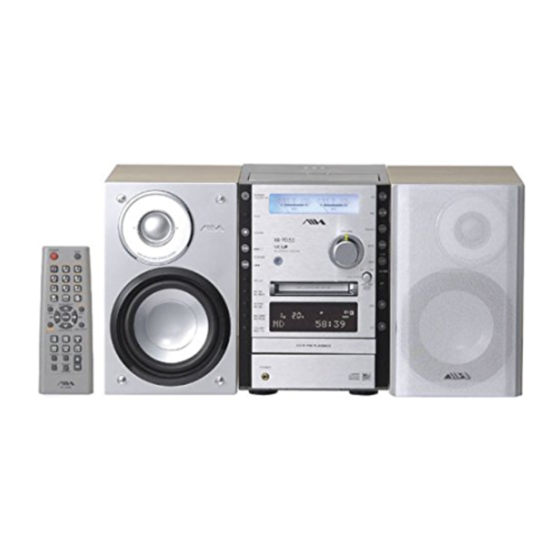
SYSTEM
XR-FD55
XR-FD55
BASIC TAPE MECHANISM : BZM-1 AR2NC
BASIC CD MECHANISM : 3ZG-3 E14NC
BASIC MD MECHANISM : MDM-16QA
CENTER UNIT
CX-LFD55
S/M Code No. 09-032-365-9R2
REMOTE
SPEAKER
CONTROLLER
SX-LFD55
RC-CAS20
CEK
Advertisement
Table of Contents

Subscribe to Our Youtube Channel
Related Manuals for Aiwa XR-FD55


Summary of Contents for Aiwa XR-FD55
- Page 1 XR-FD55 SERVICE MANUAL BASIC TAPE MECHANISM : BZM-1 AR2NC MICRO Hi-Fi COMPONENT SYSTEM BASIC CD MECHANISM : 3ZG-3 E14NC BASIC MD MECHANISM : MDM-16QA This Service Manual is “Revision Piblishing” and replaces “Simple Manual” (S/M Code No. 09-032-365-9T2). REMOTE CENTER UNIT...
-
Page 2: Table Of Contents
TABLE OF CONTENTS -1/1 PRECAUTION TO REPLACE OPTICAL BLOCK ............................. 3 SPECIFICATIONS ....................................4 ACCESSORIES PARTS LIST .................................. 5 ELECTRICAL PARTS LIST ................................6 ~ 21 TRANSISTOR ILLUSTRATION ................................21 BLOCK DIAGRAM -1/1 (LEVEL SECTION) ............................22 SCHEMATIC DIAGRAM -1/10 (MAIN-1/3 SECTION) ........................... 23 SCHEMATIC DIAGRAM -2/10 (MAIN-2/3 MD AMP SECTION) ...................... -
Page 3: Precaution To Replace Optical Block
PRECAUTION TO REPLACE OPTICAL BLOCK (PXR-104X-BP-0101) Body or clothes electrostatic potential could ruin laser diode in the optical block. Be sure ground body and workbench, and use care the clothes do not touch the diode. 1) After the connection, remove solder shown in right figure. -
Page 4: Specifications
SPECIFICATIONS -1/1 MAIN UNIT CX-LFD55 TUNER FM tuning range 87.5 MHz to 108 MHz FM usable sensitivity (IHF) 16.8 dBf 75 Ω (unbalanced) FM antenna terminal AM tuning range 531 kHz to 1602 kHz 350 µV/m AM usable sensitivity AM antenna Loop antenna AMPLIFIER Rated: 24 W + 24 W (6 Ω, T.H.D.1%, 1 kHz/DIN 45500) -
Page 5: Accessories Parts List
Components marked X and R are not designated as spare parts for after sales service, and will not be stocked at the spare parts centers. UNIT-NAME ! C REF-NO PARTS-NO PARTS-NAME SUFFIX&MODEL XR-FD55 O AS1001 8C-CJE-909-010 IB,K(E)BF XR-FD55 O AS1002 87-A92-150-110 ANT,LOOP AM NO-CONT O AS1003 87-A92-346-110 ANT,WIRE FM(FASTEN) O AS1004 8C-CJE-701-010 RC UNIT,RC-CAS20... -
Page 6: Electrical Parts List - 1/16
Components marked X and R are not designated as spare parts for after sales service, and will not be stocked at the spare parts centers. UNIT-NAME ! C REF-NO PARTS-NO PARTS-NAME SUFFIX&MODEL XR-FD55 0597 87-010-831-080 C-CAP,U 0.1-16 Z F GRM 0598 87-010-831-080 C-CAP,U 0.1-16 Z F GRM 0601 87-012-277-080 C-CAP,U 1800P-50 K B GRM 0602 87-012-277-080 C-CAP,U 1800P-50 K B GRM 0603 87-A13-163-080 CAP,E 0.33-50 M FG... - Page 7 Components marked X and R are not designated as spare parts for after sales service, and will not be stocked at the spare parts centers. UNIT-NAME ! C REF-NO PARTS-NO PARTS-NAME SUFFIX&MODEL XR-FD55 0630 87-A30-670-040 C-TR,SBT5551 0683 87-A30-162-010 FET,2SK2937 0684 87-A30-162-010 FET,2SK2937 0685 87-A30-076-040 C-TR,2SC3052F...
- Page 8 Components marked X and R are not designated as spare parts for after sales service, and will not be stocked at the spare parts centers. UNIT-NAME ! C REF-NO PARTS-NO PARTS-NAME SUFFIX&MODEL XR-FD55 0682 88-118-222-080 C-RES,S 2.2K-1/10W J 0684 88-118-102-080 C-RES,S 1K-1/10W J 0685 88-108-332-080 C-RES,U 3.3K-1/16W J 0686 88-118-222-080 C-RES,S 2.2K-1/10W J...
- Page 9 Components marked X and R are not designated as spare parts for after sales service, and will not be stocked at the spare parts centers. UNIT-NAME ! C REF-NO PARTS-NO PARTS-NAME SUFFIX&MODEL XR-FD55 0671 87-A13-118-080 CAP,E 47-16 M RA 6.3X5L 0672 87-010-831-080 C-CAP,U 0.1-16 Z F GRM 0673 87-010-831-080 C-CAP,U 0.1-16 Z F GRM 0674 87-A13-116-080 CAP,E 10-35 M RA 5X5L...
- Page 10 Components marked X and R are not designated as spare parts for after sales service, and will not be stocked at the spare parts centers. UNIT-NAME ! C REF-NO PARTS-NO PARTS-NAME SUFFIX&MODEL XR-FD55 0608 88-108-473-080 C-RES,U 47K-1/16W J 0610 88-108-123-080 C-RES,U 12K-1/16W J 0611 88-108-102-080 C-RES,U 1K-1/16W J 0612 88-108-000-080 C-JUMPER,U...
- Page 11 Components marked X and R are not designated as spare parts for after sales service, and will not be stocked at the spare parts centers. UNIT-NAME ! C REF-NO PARTS-NO PARTS-NAME SUFFIX&MODEL XR-FD55 0105 87-010-408-040 CAP,E 47-50 M 11L SME 0106 87-A12-317-080 C-CAP,U 0.1-50 Z F 0114 87-015-699-040 CAP,E 10-50 M 7L SRA 0115 87-012-274-080 C-CAP,U 1000P-50 K B GRM 0117 87-012-286-080 C-CAP,U 0.01-25 K B GRM...
- Page 12 Components marked X and R are not designated as spare parts for after sales service, and will not be stocked at the spare parts centers. UNIT-NAME ! C REF-NO PARTS-NO PARTS-NAME SUFFIX&MODEL XR-FD55 0130 87-010-831-080 C-CAP,U 0.1-16 Z F GRM 0131 87-010-831-080 C-CAP,U 0.1-16 Z F GRM 0136 87-010-831-080 C-CAP,U 0.1-16 Z F GRM 0138 87-010-831-080 C-CAP,U 0.1-16 Z F GRM...
- Page 13 Components marked X and R are not designated as spare parts for after sales service, and will not be stocked at the spare parts centers. UNIT-NAME ! C REF-NO PARTS-NO PARTS-NAME SUFFIX&MODEL XR-FD55 MAIN 0462 87-012-158-080 C-CAP,S 390P-50 J CH GRM MAIN 0463 87-010-831-080 C-CAP,U 0.1-16 Z F GRM...
- Page 14 Components marked X and R are not designated as spare parts for after sales service, and will not be stocked at the spare parts centers. UNIT-NAME ! C REF-NO PARTS-NO PARTS-NAME SUFFIX&MODEL XR-FD55 MAIN 0007 87-A40-455-080 DIODE,RL203 GW MAIN 0008 87-A40-455-080 DIODE,RL203 GW...
- Page 15 Components marked X and R are not designated as spare parts for after sales service, and will not be stocked at the spare parts centers. UNIT-NAME ! C REF-NO PARTS-NO PARTS-NAME SUFFIX&MODEL XR-FD55 MAIN 0621 87-A30-494-080 TR,2SA1980G MAIN 0622 87-A30-288-040 C-TR,DTC114YKA MAIN 0001 88-130-159-080 RES,1.5-1/4W J...
- Page 16 Components marked X and R are not designated as spare parts for after sales service, and will not be stocked at the spare parts centers. UNIT-NAME ! C REF-NO PARTS-NO PARTS-NAME SUFFIX&MODEL XR-FD55 MAIN 0248 88-130-100-080 RES,10-1/4W J MAIN 0249 88-121-100-080 RES,10-1/8W J...
- Page 17 Components marked X and R are not designated as spare parts for after sales service, and will not be stocked at the spare parts centers. UNIT-NAME ! C REF-NO PARTS-NO PARTS-NAME SUFFIX&MODEL XR-FD55 MAIN 0668 88-121-120-080 RES,12-1/8W J MAIN 0672 88-108-103-080 C-RES,U 10K-1/16W J...
- Page 18 Components marked X and R are not designated as spare parts for after sales service, and will not be stocked at the spare parts centers. UNIT-NAME ! C REF-NO PARTS-NO PARTS-NAME SUFFIX&MODEL XR-FD55 MICON 0135 87-012-174-080 C-CAP,U 12P-50 J CH GRM MICON 0137 87-012-274-080 C-CAP,U 1000P-50 K B GRM MICON 0139 87-010-831-080 C-CAP,U 0.1-16 Z F GRM...
- Page 19 Components marked X and R are not designated as spare parts for after sales service, and will not be stocked at the spare parts centers. UNIT-NAME ! C REF-NO PARTS-NO PARTS-NAME SUFFIX&MODEL XR-FD55 MICON 0152 88-108-392-080 C-RES,U 3.9K-1/16W J MICON 0153 88-108-562-080 C-RES,U 5.6K-1/16W J...
- Page 20 Components marked X and R are not designated as spare parts for after sales service, and will not be stocked at the spare parts centers. UNIT-NAME ! C REF-NO PARTS-NO PARTS-NAME SUFFIX&MODEL XR-FD55 ! O PT 0081 8B-MA6-675-010 PT,SUB BMA E (VRK) ! O RY 0081 87-A91-418-010 RELAY,AC 12V G5PA-1-M 0081 8C-CJE-608-010 WIRE ASSY,140 BLACK FASTON 0703 87-015-689-040 CAP,E 10-35 M 7L SRA...
-
Page 21: Transistor Illustration
ELECTRICAL PARTS LIST - 16/16 • Regarding connectors, they are not stocked as they are not the initial order items. The connectors are available after they are supplied from connector manufacturers upon the order is received. CHIP RESISTOR PART CODE Chip Resistor Part Coding Figure Resistor Code... -
Page 22: Block Diagram -1/1 (Level Section)
BLOCK DIAGRAM - 1/1 (LEVEL SECTION) IC101 MAIN C.B IC602 J203 SPEAKERS IC601 AMP C.B -22-... -
Page 23: Schematic Diagram -1/10 (Main-1/3 Section)
SCHEMATIC DIAGRAM - 1/10 (MAIN -1/3 SECTION) MAIN C.B 1/3 TO TUNER PACK VIA FFC604 C669 560P 50V KB C676 TO MAIN C.B 2/3 0.1 16V ZF (MD AMP SECTION) 3A-7A C670 560P 50V KB DIGITAL IN (OPTICAL) TO MAIN C.B 3/3 TO USB C.B CN701 VIA FFC607 (LEVEL METER SECTION) 2B-9B... -
Page 24: Schematic Diagram -2/10 (Main-2/3 Md Amp Section)
SCHEMATIC DIAGRAM -2/10 (MAIN-2/3 MD AMP SECTION) MAIN C.B 2/3 (MD AMP SECTION) :AUDIO (PB) SIGNAL -24-... -
Page 25: Schematic Diagram -3/10 (Main-3/3 Level Meter Section)
SCHEMATIC DIAGRAM -3/10 (MAIN-3/3 LEVEL METER SECTION) MAIN C.B 3/3 (LEVEL METER SECTION) -25-... -
Page 26: Schematic Diagram -4/10 (Hp Section)
SCHEMATIC DIAGRAM -4/10 (HP SECTION) HP C.B PHONES :AUDIO (PB) SIGNAL -26-... -
Page 27: Wiring -1/8 (Main C.b, Hp C.b)
WIRING - 1/8 (MAIN C.B/HP C.B) TO TUNER PACK TO USB C.B CN701 TO CD C.B CN602 TO MICON C.B CN115 TO HEAD C.B CNA302 MAIN C.B FB603 R043 R045 R044 CN604 CN602 R685 R616 CN607 R686 R698 C636 C634 D632 R696 R626... -
Page 28: Schematic Diagram -5/10 (Amp Section)
SCHEMATIC DIAGRAM - 5/10 (AMP SECTION) Q603,605,607,609 Q611,615 Q613,627 Q617,619 Q623 DIFFERENTIAL AMP CURRENT TO VOLTAGE AMP BIAS CIRCUIT POWER AMP OVERLOAD DET AMP C.B Q613,627 C609 100P 50V J CH MUTE Q615 SBT5551 MUTE MUTE Q614,628 C610 100P 50V J CH Q626,630 HOLD Q624... -
Page 29: Wiring -2/8 (Amp C.b)
WIRING - 2/8 (AMP C.B) AMP C.B Q627 Q628 Q620 C617 R672 R671 Q619 C618 R676 Q617 R675 Q618 TH602 R673 R674 TH601 Q614 Q613 R637 Q623 D650 R633 R638 R631 R635 R634 D607 R630 R629 C611 R560 R636 D605 R632 R625 Q624... -
Page 30: Schematic Diagram -6/10 (Usb Section)
SCHEMATIC DIAGRAM -6/10 (USB SECTION) USB C.B FB708 USB DAC -30-... -
Page 31: Wiring -3/8 (Usb C.b)
WIRING - 3/8 (USB C.B) USB C.B R741 Q703 C725 R704 J701 D703 Q702 J701 C703 R740 C717 FFC607 R711 C715 FB707 R737 R708 C720 FB705 CN701 C719 R709 R710 R707 C706 X701 IC701 FB706 C705 C727 R738 R716 JR710 C711 C713 C718... -
Page 32: Schematic Diagram -7/10 (Micon/Deck Section)
SCHEMATIC DIAGRAM - 7/10 (MICON/DECK SECTION) TO METER C.B CN109 VIA FFC112 TO KEY C.B CN108 VIA FFC114 TO MAIN C.B 1/3 CN608 VIA FFC115 MICON C.B PIN2 C806 (GND) 8.2P (CLK) IC102 R137 LC8752B2A-50Y2 C805 C803 8.2P 8.2P C804 8.2P DECK C.B DN6851... -
Page 33: Schematic Diagram -8/10 (Key/Meter/Led Section)
SCHEMATIC DIAGRAM - 8/10 (KEY/METER/LED SECTION) KEY C.B (DISPLAY) METER C.B (LEVEL METER) MULTI JOG PUSH ENTER /DEMO LED C.B D105,106 GROUP / PRESET (LEVEL METER LIGHTING) VOLUME IC103 (REMOTO SENSOR) C122 100P 50V J CH -33-... -
Page 34: Wiring -4/8 (Micon C.b/Key C.b/Meter C.b/Led C.b)
WIRING - 4/8 (MICON C.B/KEY C.B/METER C.B/LED C.B) LED C.B D106 METER C.B MICON C.B R274 R272 D105 R275 Q114 JR101 R188 R187 JR102 R273 R271 R198 R186 TO DECK C.B CN1 TO CD C.B CN603 Q106 Q104 CN109 CN106 Q115 D105,106 R283... -
Page 35: Wiring -5/8 (Deck C.b/Head C.b)
WIRING -5/8 (DECK C.B/HEAD C.B) DECK C.B TO MICON C.B CN116 FFC116 CRD1 RPH/EH HEAD C.B CNA302 TO MAIN C.B CN302 -35-... -
Page 36: Schematic Diagram -9/10 (Cd Section)
SCHEMATIC DIAGRAM - 9/10 (CD SECTION) CD C.B 470P 4.7M C697 3.3P C696 C695 C699 3.3P 3.3P 0.22 2SA1981Y FB602 FB601 470P F-BEAD F-BEAD BL02RN2 BL02RN2 1200P C694 W602 3.3K TO CHASSIS 50V J CH CON2 CON3 (OPEN) CD DRIVE C.B CD TRAY C.B -36-... -
Page 37: Wiring -6/8 (Cd C.b)
WIRING - 6/8 (CD C.B) TO PICK UP ASSY CD C.B C519 R503 TO CHASSIS C504 C515 R557 FFC502 CN601 C614 C513 W602 C506 C501 R501 JR601 C685 FFC110 CN602 R504 C503 C684 C551 C683 Q601 C682 C554 FFC602 C603 R601 C681 R602... -
Page 38: Wiring -7/8 (Cd Drive C.b/Cd Tray C.b)
WIRING - 7/8 (CD DRIVE C.B/CD TRAY C.B) TO CD C.B CN502 CD DRIVE C.B FFC502 CON2 CD TRAY C.B CON3 FFC503 TO CD C.B CN503 -38-... -
Page 39: Schematic Diagram -10/10 (Pt Section)
SCHEMATIC DIAGRAM -10/10 (PT SECTION) PT C.B PT,K CCJ-E PT,SUB BMA E (VRK) AC230V,50Hz -39-... -
Page 40: Wiring -8/8 (Pt C.b)
WIRING - 8/8 (PT C.B) TO MAIN C.B 1/3 WH001 PT C.B D081 RY081 CN081 AC230V,50Hz PR081 C086 C087 D085 C081 D083 D082 D084 PT081 JW086 JW087 JW088 JW085 CN082 PR082 C085 W081 TO SHASSIS -40-... -
Page 41: Electrical Adjustment
ELECTRICAL ADJUSTMENT -1/5 <DECK Section> MAIN C.B (PATTERN SIDE) SFR452 SFR451 MOTOR SFR DECK MOTOR -41-... -
Page 42: Deck Section
ELECTRICAL ADJUSTMENT -2/5 <DECK SECTION> Make the following preparations for DECK adjustment. Preparations • Measuring instruments: Audio signal oscillator/Attenuator/Wow-Flutter meter (frequency counter)/Oscilloscope/Millivoltmeter/Dummy resistance (6Ω) • Test Tape: TTA-100 / TTA-330/ TTA-200 / TTA-602 (or equivalent test tape for play/record) 1. Tape Speed Adjustment and Check Requirements Measuring instruments: Wow-flutter meter (frequency counter) Test tape: TTA-100 (3 kHz) - Page 43 ELECTRICAL ADJUSTMENT -3/5 5. Playback Sensitivity Check Requirements Measuring instrument: Millivoltmeter Test tape: TTA-200 (400 Hz) Test point: TP8 (Rch), TP9 (Lch) (1) Connect the CH1 of millivoltmeter to TP9 (Lch) and the CH2 to TP8 (Rch). (2) Insert the test tape (TTA-200) to DECK to playback. (3) Check that the output level is ranged within 145 mV ±...
- Page 44 ELECTRICAL ADJUSTMENT -4/5 <FRONT Section> MICON C.B (PARTS SIDE) JW150 L102 JW149 PIN2 (CLK) (GND) <FRONT SECTION> 8. Clock Adjustment Requirement Measuring instrument: Frequency counter Test point: TP1 (CLK), PIN2 (GND) Adjustment point: L102 (1) While pressing and holding down the POWER button and the TUNER button, insert the AC plug. (2) Adjust L102 so that the frequency counter indicates 176.83 ±...
-
Page 45: Electrical Adjustment
ELECTRICAL ADJUSTMENT -5/5 CD C.B (PATTERN SIDE) IC501 IC505 R515 IC601 <CD AAdjustment> • Adjust and check at test mode. • Keep at a level CD Mechanism. • Equipment Measure: Oscilloscope (using probe 10:1) Digital Multimeter (using at DCV range) Jitter Meter (KIKUSUI 6235) Test Disc: TCD-782/ATD-001 1. -
Page 46: Cd Test Mode
CD TEST MODE -1/1 1. Starting CD Test Mode While pressing and holding down the CD FUNCTION button, insert the AC plug to outlet. When test mode starts, the message, CD TEST appears on the display, and all indicators light. 2. -
Page 47: Fl Display (15-Bt-89Gink)
FL DISPLAY -1/1 <15-BT-89GINK> GRID ASSIGNMENT ANODE CONNECTION PIN CONNECTION -47-... -
Page 48: Ic Block Diagram
IC BLOCK DIAGRAM -1/3 IC, M61518FP PB-N(L) REC-O(L) PB-P(L) REC-N(L) REC-N(R) PB-P(R) REC-O(R) PB-N(R) C-IN(R) C-IN(L) B-IN(R) PB-OUT(R) B-IN(L) PB-OUT(L) A-IN(R) VOL-IN(L) A-IN(L) VOL-IN(R) OUT(L) OUT(R) TRE-I(L) TRE-O(L) TRE-I(R) BASS-O(R) TRE-O(R) MID-I(L) BASS-I(R) BASS-O(L) MID-O(L) MID-I(R) BASS-I(L) MID-O(R) CONT -48-... - Page 49 IC BLOCK DIAGRAM -2/3 IC, PCM2702E/2K 25 24 17 18 Packet Audio Data Data Low-Pass Multi- Filter FIFO Level Delta- wrclk Digital Filter Sigma Modulator Low-Pass DGNDU Filter mclk System Clock Audio Clock Clock SpAct Generator Generator DGNDC Crystal Power Supply DGNDP AGND DGND...
-
Page 50: Ic Block Diagram
IC BLOCK DIAGRAM -3/3 IC, PCM1742KE Audio LRCK Output Amp and Serial Port Low-Pass Filter 4x/8x DATA Enhanced Oversampling Multilevel Digital Filter Delta-Sigma with Modulator Function MLAT Controller Output Amp and Serial Control MCLK Low-Pass Filter Port MDATA System Clock System Clock Power Supply Zero Detect... -
Page 51: Ic Description
IC DESCRIPTION -1/2 (LC8752B2A-50Y2) -1/3 Pin No. Pin Name Description O-CDT CLOSE CD tray close output O-CDT OPEN CD tray open output O-CD-RESET CD reset output I-CD-BLKCK CD sub-code clock input I-CD-SENSE CD sense input ________ O-CDX4 – Not used I-RMC Remote control sensor data input _______... - Page 52 IC DESCRIPTION -1/2 (LC8752B2A-50Y2) -2/3 Pin No. Pin Name Description I-AS Pulse input for TAPE couter I-HEAD Input of detection in TAPE head position O-PL TAPE plunger control output O-MOTOR TAPE motor power supply ON/OFF control output O-LED1(BLUE) FL back-light control output O-LED2(RED) FL back-light control output O-SI(FL)
- Page 53 IC DESCRIPTION -1/2 (LC8752B2A-50Y2) -3/3 Pin No. Pin Name Description O-PLL DO TUNER data output I-TU SELECT1 Detection in TUNER force I-TU SELECT2 Detection in TUNER force VSS3 – Ground VDD3 – Power supply – Not connected (CLK) – Not connected (DATA) –...
- Page 54 IC DESCRIPTION -2/2 (MN6627482WA) -1/2 Pin No. Pin Name Description BCLK Bit clock output for SRDATA LRCK Distinction L and R signal output SRDATA Serial data output DVDD1 Power supply for digital circuit DVSS1 GND for digital circuit Digital audio interface output signal MCLK Microcomputer command clock input (Data is latched at starting edge) MDATA...
-
Page 55: Ic Description
IC DESCRIPTION -2/2 (MN6627482WA) -2/2 Pin No. Pin Name Description TOFS – Not connected WVEL – Not connected RF signal input IREF Standard current input terminal Bias singal for DSL DSLF Roop filter signal for DSL PLLF Roop filter signal for PLL VCOF Roop filter signal for VCO AVDD2... -
Page 56: Disassembly
DISASSEMBLY -1/5 1. PLATE, L/R 1) Release 4 screws (BVT2+3-8 SILVER) of PLATE, R. 2) Remove PLATE, R with sliding to rear side. 3) Remove PLATE,L with same way. PLATE, R 2. PANEL, TOP ASSY (DECK MECHANISM) 1) Remove the wirer of DECK. 2) Release one screw (BVT2+3-8 SILVER) of PANEL,TOP ASSY. - Page 57 DISASSEMBLY -2/5 3. CABI, REAR ASSY 1) Remove TUNER PACK and FFC of USB UNIT. 2) Release 8 screws (BVT2+3-8 BLACK) of CABI, REAR ASSY. CABI, REAR ASSY 4. MAIN C.B 1) Remove 3 FFCs and one connector of MAIN C.B. 2) Release 2 screws (BVT2+3-10) of MAIN C.B.
- Page 58 DISASSEMBLY -3/5 5. CABI, FRONT ASSY 1) Remove 2 FFCs of CABI, FRONT ASSY. 2) Release 2 screws (QT2+3-10, BVT2+3-6) from the bottom of CABI, FRONT ASSY. 3) Release 4 screws (QT2+3-6) from the side of CABI, FRONT ASSY. 4) Push CAM,SLIDE to the left side of CD Mechanism. 5) Pull CAM,SLIDE from the right side of CD Mechansim, and then CD tray appears.
- Page 59 DISASSEMBLY -4/5 6. MICON C.B 1) Remove FFC of MD Mechansim and FFC of CD C.B, and remove connector. 2) Release 4 screws (BVT2+3-10) of MICON C.B. MICON C.B CONNECTOR CD C.B MICON C.B 7. MD MECHANISM 1) Release 2 screws (BVTT+3-8) of CHAS, MD. MD Mechanism 8.
-
Page 60: Disassembly
DISASSEMBLY -5/5 9. SERVICE POSITION OF MDMECHANSIM 1) Remove MD MEHCANISM with referring to the disassembly procedure form 1 to 4 and from 6 to 7. 2) Set up with keeping MD MECHANISM is removed. 3) Connect MICON C.B to MD MECHANISM with extension FFC. Parts No. -
Page 61: Mechanical Exploded View
MECHANICAL EXPLODED VIEW -1/1 -61-... -
Page 62: Mechanical Parts List
Components marked X and R are not designated as spare parts for after sales service, and will not be stocked at the spare parts centers. UNIT-NAME ! C REF-NO PARTS-NO PARTS-NAME SUFFIX&MODEL XR-FD55 O MC1001 8C-CJE-003-010 PANEL,TOP O MC1002 8C-CJE-004-010 PANEL,L... -
Page 63: Color Name Table
Components marked X and R are not designated as spare parts for after sales service, and will not be stocked at the spare parts centers. UNIT-NAME ! C REF-NO PARTS-NO PARTS-NAME SUFFIX&MODEL XR-FD55 X MC1079 8C-CJE-634-010 PWB,HP O MC1A 87-067-703-010 BVT2+3-10 W/0 SL0T... -
Page 64: Tape Mechanism Exploded View
TAPE MECHANISM EXPLODED VIEW -1/1 <BZM-1 AR2NC> -64-... -
Page 65: Tape Mechanism Parts List
TAPE MECHANISM PARTS LIST -1/2 <BZM-1 AR2NC> = ! SAFTY PARTS = Components marked All components used on this model at the production line are shown in this service manual. However, please note that not all components will be available as spare parts for after-sales service. Components marked S and O are designated as spare parts for service and will be stocked at the spare parts centers. - Page 66 TAPE MECHANISM PARTS LIST -2/2 <BZM-1 AR2NC> = ! SAFTY PARTS = Components marked All components used on this model at the production line are shown in this service manual. However, please note that not all components will be available as spare parts for after-sales service. Components marked S and O are designated as spare parts for service and will be stocked at the spare parts centers.
-
Page 67: Cd Mechanism Exploded View <3Zg-3 E14Nc
CD MECHANISM EXPLODED VIEW -1/2 <3ZG-3 E14NC> -67-... -
Page 68: Cd Mechanism Parts List <3Zg-3 E14Nc
CD MECHANISM PARTS LIST -1/2 <3ZG-3 E14NC> = ! SAFTY PARTS = Components marked All components used on this model at the production line are shown in this service manual. However, please note that not all components will be available as spare parts for after-sales service. Components marked S and O are designated as spare parts for service and will be stocked at the spare parts centers. -
Page 69: Cd Mechanism Exploded View
CD MECHANISM EXPLODED VIEW -2/2 <CZG-8 YA1NC> -69-... -
Page 70: Cd Mechanism Parts List
CD MECHANISM PARTS LIST -1/1 <CZG-8 YA1NC> = ! SAFTY PARTS = Components marked All components used on this model at the production line are shown in this service manual. However, please note that not all components will be available as spare parts for after-sales service. Components marked S and O are designated as spare parts for service and will be stocked at the spare parts centers. -
Page 71: General Speaker Disassembly Instructions (For Reference)
GENERAL SPEAKER DISASSEMBLY INSTRUCTIONS (FOR REFERENCE) -1/1 Type.1 Type.4 Insert a flat-bladed screwdriver into the position indicated by the TOOLS arrows and remove the panel. Remove the screws of each speaker Plastic head hammer unit and then remove the speaker units. ) flat head screwdriver Cut chisel How to Remove the PANEL, FR... -
Page 72: Speaker Parts List (Sx-Lfd55)
Components marked X and R are not designated as spare parts for after sales service, and will not be stocked at the spare parts centers. UNIT-NAME ! C REF-NO PARTS-NO PARTS-NAME SUFFIX&MODEL SX-SLFD55 X SP1001 8C-CPE-851-010 CTN,ASSY TTC X SP1002 8C-CPE-029-010 BADGE,AIWA 25 NEW X SP1003 8C-CP2-013-010 BOSS,CATCHER X SP1004 8C-CPE-002-010 CABI,M O SP1005 8C-CPE-033-010 CORD,SPKR 2.5M X SP1006 8C-CPE-013-010 FASTENER,CL... -
Page 73: Other Parts List
Components marked X and R are not designated as spare parts for after sales service, and will not be stocked at the spare parts centers. UNIT-NAME ! C REF-NO PARTS-NO PARTS-NAME SUFFIX&MODEL XR-FD55 87-B40-057-010 BAG,PP 0.03-150-200 87-B40-095-010 BAG,PV 0.04-500-550 PL 8C-CJE-851-010 CUSHION,FRONT C 8C-CJE-852-010 CUSHION,REAR C 93-324-066-010 SH,FOAMED-MAT 0.31-500-300... -
Page 74: Md Mechanism (Mdm-16Qa)
MD-MECHANISM (MDM-16QA) SERVICE MANUAL MD MECHANISM BASIC MD MECHANISM : MDM-16QA -74-... -
Page 75: Protection Eyes From Laser Beam During Servicing
PROTECTION EYES FROM LASER BEAM DURING SERVICING -1/1 Precaution to replace Optical block Body or clothes electrostatic potential could ruin laser diode in the optical block. Be sure ground body and workbench, and use care the clothes do not touch the diode. 1) After pulling out the flexible board for optical pickup from the connector, cover the tip of flexible board with conductive aluminum foil, etc., in order to prevent static electricity from damaging the pickup. -
Page 76: Disassembly Instruction
DISASSEMBLY INSTRUCTIONS -1/3 Disassembly Cautions before disassembly: When disassembling this unit and reassembling it after repair, be careful of the following to ensure safety and reliable performance: 1. Remove the mini-disc from this unit. 2. Take great care not to use screws of greater lengths when installing MD mechanism block (screws that secure components to be installed in MD block mechanism chassis): A longer screw will contact the optical pickup, which could result in no operation. - Page 77 DISASSEMBLY INSTRUCTIONS -2/3 (37)x2 ø2x3mm SHIELD COVER, TOP (25) PLATE, EARTH(3)x1 INSULATORS(27)x2 MD MECHANISM Soldered (2*) SPRING, EARTH MD MAIN C.B pointsx2 (15)x1 Soldered pointsx2 Soldered pointsx4 Main C.B Pull out Pull out Soldered Flexible Board for pointsx5 (38)x2 (38)x1 Optical Pickup (*1) ø...
-
Page 78: Disassembly Instruction
DISASSEMBLY INSTRUCTIONS -3/3 Step Item Tool Caution (2) Procedure up to spindle motor removal 1) Removing SPINDLE MOTOR (M903) (Fig. 3-1) Remove 3 screws (34). Screwdriver Remove SPINDLE MOTOR (M903). (3) Procedure up to loading motor removal 1) Removing LOADING MOTOR (M902) (Fig. 3-2) Remove screw (36) holding ANGLE, LD MOTOR (2). - Page 79 ELECTRICAL PARTS LIST -1/4 = ! SAFTY PARTS = Components marked All components used on this model at the production line are shown in this service manual. However , please note that not all components will be available as spare parts for after-sales service. Components marked S and O are designated as spare parts for service and will be stocked at the spare parts centers.
-
Page 80: Electrical Parts List
ELECTRICAL PARTS LIST -2/4 = ! SAFTY PARTS = Components marked All components used on this model at the production line are shown in this service manual. However , please note that not all components will be available as spare parts for after-sales service. Components marked S and O are designated as spare parts for service and will be stocked at the spare parts centers. - Page 81 ELECTRICAL PARTS LIST -3/4 = ! SAFTY PARTS = Components marked All components used on this model at the production line are shown in this service manual. However , please note that not all components will be available as spare parts for after-sales service. Components marked S and O are designated as spare parts for service and will be stocked at the spare parts centers.
-
Page 82: Transistor Illustration
ELECTRICAL PARTS LIST -4/4 • Regarding connectors, they are not stocked as they are not the initial order items. The connectors are available after they are supplied from connector manufacturers upon the order is received. CHIP RESISTOR PART CODE Chip Resistor Part Coding Figure Resistor Code Value of resistor... -
Page 83: Block Diagram -1/1
BLOCK DIAGRAM -1/1 TO MICON C.B 1 2 3 4 5 6 7 8 9 10 11 12 13 14 15 16 17 18 19 20 21 22 23 24 25 26 27 28 CN1501 MAIN C.B HEAD MECH AN ISM 4.75~5.25V 4.75~5.25V MECHANISM... -
Page 84: Schematic Diagram -1/1
SCHEMATIC DIAGRAM -1/1 MAIN C.B C1205 C1114 0.033 C1117 C1118 0.47 C1113 C1115 0.033 C1119 : WAVEFORMS No. R1119 0.47 220K 0.7 1.1 1.3 1.3 1234 VCC1 C1201 EFMAGC DADATA C1123 DCNF ADDATA EFMO EFMI ADDATA R1211 & C1211 0.1 DFCK ADAGI C1121... -
Page 85: Wiring -1/2
WIRING -1/2 (MAIN C.B) MAIN C.B (Top view) MAIN C.B (Bottom view) To MICON C.B CN1501 FL1524 FL1523 C1536 R1540 C1563 R1530 C1534 FL1518 C1508 FL1525 HEAD C1540 C1538 C1611 C1304 IC1302 R1516 R1616 D1300 R1300 CW901 R1716 M902 L1300 C1340 LOADING CW902... -
Page 86: Wiring -2/2
WIRING - 2/2 (LOADING C.B/LEAD IN C.B) LOADING C.B SW1933 (REC) SW1934 SW1934 (PLAY) SW1933 SW1932 SW1932 (LOAD) To MAIN (Bottom view) C.B CW1931 CW1932 CW1933 LEAD IN C.B CW1935 CW1934 R1932 R1931 SW1930 SW1930 (WRITE PRO) SW1936 SW1936 (LEAD IN) -86-... -
Page 87: Waveforms
WAVEFORMS -1/2 TOC READ (low-reflection disc) POWER ON Stopped (500ms/div) CH1=5.0V CH2=2.0V CH3=2.0V CH4=2.0V 10:1 10:1 10:1 10:1 TP1122 TP1509 (F+) (DVDD) TP1800 TP1207 (3.2V) (TEMON) TP1603 TP1518 (SP+) (RESET) TP1602 TP1511 (SP-) (PCONT0) TOC READ (high-reflection disc) TOC READ (low-reflection disc) TP1122 TP1122 (F+) -
Page 88: Waveforms
WAVEFORMS -2/2 PLAY (low-reflection disc) TP1201 (EFMMON) TP1300 (REC HEAD) TP1207 (TEMON) TP1302 (EFMO) TP1121 (T+) TP1105 (LDVAR) TP1421 (CIN) TP1113 (R/P) PLAY (high-reflection disc) Analog REC TP1201 (EFMMON) IC1201 (DFCK) TP1207 (TEMON) IC1201 (ADDATA) TP1121 (T+) IC1201 (BCLK) TP1421 (CIN) IC1201 (LRCK) -
Page 89: Adjustment
ADJUSTMENT -1/13 MD Adjustment Depending on the content of repair, such as when the new mechanism, pickup and MD C.B. are combined, the test mode must be set, and various adjustments may be required. The adjustment procedure is as follows: (1) Set to the test mode and perform the adjustment and check listed below depending on the component replaced. - Page 90 ADJUSTMENT -2/13 2. Test mode Setting to test mode: 1. While holding down the MD key, plug the power cord into AC outlet. 2. Load disc 1 for playback (high-reflection disc) or a disc for recording (low-reflection disc) (will enter the (D) status). (A) EJECT : EJECT status (B) tsm26...
- Page 91 ADJUSTMENT -3/13 1. EJECT mode Step No. Setting method Remarks Display Test mode EJECT status Pressing STOP button will return to step 1 from each other step. [ _ _ _ _ _ E J E C T _ _ _ _ _ ] [ p p w _ _ _ _ _ _ _ _ _ _ _ _ ] Press SP/LP button Playback power output status...
- Page 92 ADJUSTMENT -4/13 2. AUTO main adjustment mode Use disc for main adjustment (MDW-74/GA-1). Step No. Setting method Remarks Display [tsm26 Test mode STOP status Press CD SYNC button AUTO adjustment menu [AUTO_AJST_] [_AUT_YOBI_] Press CD SYNC button AUTO preliminary adjustment menu [ *********** ] Press ENTER (MULTI JOG) •...
- Page 93 ADJUSTMENT -5/13 5. EEPROM setting mode (when writing data to EEPROM, press the POWER button before resetting.) a) Focus setting Step No. Setting method Display [ t s m 2 6 Test mode STOP status [ E E P R O M _ S E T ] Press CD SYNC button 3 times Press ENTER button [ _ _ F o c u s _ _ _ ]...
- Page 94 ADJUSTMENT -6/13 [TG2______ Press CD SYNC button [TF0______ Press CD SYNC button Press CD SYNC button [TF02_____ [TF1______ Press CD SYNC button Press CD SYNC button [TF12_____ Press CD SYNC button [TF2______ Press CD SYNC button [TF22_____ Press CD SYNC button [FT3______ Press CD SYNC button [SVCNT4__...
- Page 95 ADJUSTMENT -7/13 e) TEMP setting Step No. Setting method Display [ _ _ _ E J E C T _ _ _ ] EJECT status (or in no mechanism status) Press REC START button [TEMP_ • : Setting value; : Measured value f) CONTROL setting Step No.
- Page 96 ADJUSTMENT -8/13 g) ADJUST setting Step No. Setting method Display [tsm26 Test mode STOP status [ E E P R O M _ S E T ] Press CD SYNC button 3 times Press ENTER button [ _ _ F o c u s _ _ _ ] [ _ A D J S E T _ _ _ ] Press CD SYNC button 6 times Press ENTER button...
- Page 97 ADJUSTMENT -9/13 6. TEST-PLAY mode (Used to check playback performance with designated address) Step No. Setting method Remarks Display Test mode STOP status [ t s m 2 6 [ T E S T _ P L A Y _ ] Press REC START button TEST-PLAY menu [ A D R E S _ 0 0 3 2 _ ]...
- Page 98 ADJUSTMENT -10/13 Lead-in switch position measurement mode Load TDYS-1 high-reflection test disc. Note: Adjust the lead-in switch position so that the value measured in INNER mode is FF85–FFD8. 1. Loosen the screw (36) holding the mechanism switch C.B. 2. If the lead-in switch position is FF85 or lower before the screw is loosened, tighten the screw while pushing the C.B. in the direction of A;...
- Page 99 ADJUSTMENT -11/13 Mechanism adjustment 1. Optical pickup grating adjustment Oscilloscope IC1201 pin 88 GND (TP1201) 100K IC1201 pin 11 EIN (TP1253) 470p GND CH1 CH2 470p IC1201 pin 12 FIN (TP1254) 100K Lissajou's figure a:b = Within 5:1 Fig. 14-1 Optical Pickup Grating Drift Measurement Method After performing auto adjustment in AUTO test mode using the TDYS-1 high-reflection disc (COMPLETE displayed), the TEST-PLAY mode will be entered: Adjust the Lissajou's figure...
- Page 100 ADJUSTMENT -12/13 Procedure for writing data to EEPROM 1. Reference temperature setting method (Perform this setting quickly with C.B. unheated at room temperature 21-29°C.) Step Details of work Display After replacing EEPROM, wait until the mechanism cools down. Connect the unassembled main C.B. to the system unit. Set to the test mode.
-
Page 101: Adjustment
ADJUSTMENT -13/13 List of data in EEPROM (version 01) Focus setting Slide setting Item display Setting value Item display Setting value [SLG______ [FG_______ [FG2______ [SL2______ [ F F 0 _ _ _ _ _ _ [SLDLIM__ [ F F 0 2 _ _ _ _ _ [SLDLEV__ [ S L K L V k _ _ [ F F 1 _ _ _ _ _ _... -
Page 102: Ic Block Diagram
IC BLOCK DIAGRAM -1/2 IC, IX2960AF Timimg Generator Timimg Generator Write Clock Data Input Generator Buffer Internal Refresh Address Counter Control Clock DQ1~DQ4 Row Address Memory Row Decoder Word Driver Buffer Cell Row Address Column Decoder Sense Amp. Buffer On ChipVBB Data Output Generator Selection... - Page 103 IC BLOCK DIAGRAM -2/2 IC, CPH5608 IC, MCH6616 IC, UDA1345TS V ref(A) V DDA(ADC) V SSA(ADC) V ADCP V ADCN 0dB/6dB VINL VINR switch V DDD DECMATION FILTER UDA1347 V SSD DC-CANCELLATION FILTER DATAO DIGITAL L3-BUS INTERFACE INTERFACE DATAI SYSCLK DSP FEATURES INTERPOLATION FILTER NOISE SHAPER...
-
Page 104: Ic Description
IC DESCRIPTION -1/3 (IX0520AW -1/3) Pin No. Pin Name Description Not Use Not Use LDVAR Laser power control output ADJS Automatic adjustment step output Track count signal input Not Use UNLOCK Unlock of Monitor PLL BYTE CNVss At usually, the time (L)/At the time of serial writing (H) DFS0 DFS0 output DFS1... - Page 105 IC DESCRIPTION -1/3 (IX0520AW -2/3) Pin No. Pin Name Description REC/PLAY change output LDON Laser diode-on output FLASH H At the time of flash writing (H) SGAIN SGAIN output DISC DISC output HFON High frequency superposition output 4M/16M DRAM selection input Unit type discernment input SYRS MDLSI register selection signal output...
- Page 106 IC DESCRIPTION -1/3 (IX0520AW -3/3) Pin No. Pin Name Description TEST1 Special mode setting input 1 TEST0 Special mode setting input 0 AVCK3 Motor driver power supply monitor input AVCK2 ADC/DAC power supply monitor input AVCK1 Head circuit power supply monitor input DTEMP Temperature sensor in-and-out power MINF...
- Page 107 IC DESCRIPTION -2/3 (IR3R58M -1/2) Pin No. Pin Name Description RF signal input terminal 1 RF signal output of a pickup is inputted. RF signal input terminal 2 RF signal output of a pickup is inputted. RF signal input terminal 3 RF signal output of a pickup is inputted. RF signal input terminal 4 RF signal output of a pickup is inputted.
- Page 108 IC DESCRIPTION -2/3 (IR3R58M -2/2) Pin No. Pin Name Description PITG It is a grounding terminal at the time of a pit. It is the resistance addition output terminal of RF3 and RF4 at the time of a groove. RF signal AGC amplifier reversed input terminal It is the resistance addition output terminal of RF1 and RF2 at the time of a groove.
- Page 109 IC DESCRIPTION -3/3 (LR37816A -1/3) Pin No. Pin Name Description EFMMON EFM monitor output AVCC1 Analog power supply (EFM system 8AD and for 8DA) EFMI The EFM signal input from RF amplifier AGND1 Analog GND AVCC2 Analog power supply (for servo system and ADIP system 1bit AD) VREF The standard voltage input of RF amplifier ADIP wobble signal...
- Page 110 IC DESCRIPTION -3/3 (LR37816A -2/3) Pin No. Pin Name Description RAWEX The data write enable signal output to external D-RAM RAD1 Data input and output with Exterior D-RAM. D1 RAD0 Data input and output with Exterior D-RAM. D0 (LSB ) RAA11 ADR11 (MSB 64Mbit) ACRCER...
-
Page 111: Ic Description
IC DESCRIPTION -3/3 (LR37816A -3/3) Pin No. Pin Name Description VDD2 The power supply for interfaces DGND Digital GND RSTX Chip reset input. It resets by active Lo. SYD0 The data bus terminal of a system control interface. (LSB) SYD1 The data bus terminal of a system control interface. -
Page 112: Mechanism Exploded View
MECHANISM EXPLODED VIEW -1/1 -112-... -
Page 113: Mechanism Parts List
MECHANISM PARTS LIST -1/1 = ! SAFTY PARTS = Components marked All components used on this model at the production line are shown in this service manual. However , please note that not all components will be available as spare parts for after-sales service. Components marked S and O are designated as spare parts for service and will be stocked at the spare parts centers. -
Page 114: Other Parts List
OTHER PARTS LIST -1/1 = ! SAFTY PARTS = Components marked All components used on this model at the production line are shown in this service manual. However , please note that not all components will be available as spare parts for after-sales service. Components marked S and O are designated as spare parts for service and will be stocked at the spare parts centers.
Need help?
Do you have a question about the XR-FD55 and is the answer not in the manual?
Questions and answers