Aiwa XR-M88 Service Manual
Compact disc stereo system
Hide thumbs
Also See for XR-M88:
- Operating instructions manual (76 pages) ,
- Service manual (58 pages) ,
- Service manual (58 pages)
Table of Contents
Advertisement
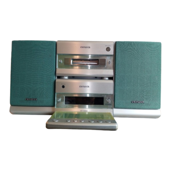
SERVICE MANUAL
COMPACT DISC STEREO SYSTEM
SYSTEM
XR-M88
XR-M89
This Service Manual is the "Revision Publishing" and replaces "Simple Manual"
(S/M Code No.09-996-333-3T2).
• BASIC TAPE MECHANISM : TN-708C-128R
• BASIC CD MECHANISM : KSM-620AAA
RECEIVER
RX-LM88
RX-LM89
S/M Code No. 09-996-333-3R2
XR-M88
XR-M89
CD/
SPEAKER
CASSETTE
FD-LM88
SX-LM200
FD-LM89
SX-LM200
K(S)
EZ(S)
Advertisement
Table of Contents


Need help?
Do you have a question about the XR-M88 and is the answer not in the manual?
Questions and answers