Table of Contents
Advertisement
Quick Links
SERVICE MANUAL
Ver 1.0 2001. 02
HCD-CL5MD is the tuner, deck, CD, MD and
amplifier section in CHC-CL5MD.
Amplifier section
AEP model:
DIN power output (Rated): 40 + 40 watts
Continuous RMS power output (Reference):
Music power output (Reference):
Other models:
DIN power output (Rated): 40 + 40 watts
Continuous RMS power output (Reference):
Inputs
VIDEO (AUDIO) IN (phono jacks):
Sony Corporation
9-929-583-11
2001B1600-1
Audio Entertainment Group
© 2001.2
General Engineering Dept.
HCD-CL5MD
Model Name Using Similar Mechanism
CD Mechanism Type
CD
SECTION
Base Unit Type
Optical Pick-up Type
Model Name Using Similar Mechanism
MD
MD Mechanism Type
SECTION
Optical Pick-up Type
Model Name Using Similar Mechanism
TAPE DECK
SECTION
Tape Transport Mechanism Type
SPECIFICATIONS
(6 ohms at 1 kHz, DIN)
50 + 50 watts
(6 ohms at 1 kHz, 10%
THD)
95 + 95 watts
(6 ohms at 1 kHz, 10%
THD)
(6 ohms at 1 kHz, DIN)
50 + 50 watts
(6 ohms at 1 kHz, 10%
THD)
voltage 250 mV,
impedance 47 kilohms
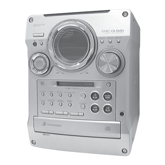
MICRO HiFi COMPONENT SYSTEM
Australian Model
CD DIGITAL IN (Supported sampling frequencies:
32 kHz, 44.1 kHz and 48 kHz)
Outputs
PHONES (stereo minijack):
accepts headphones of
8 ohms or more.
SPEAKER:
accepts impedance of 6 to
16 ohms.
CD player section
System
Compact disc and digital
audio system
Laser
Semiconductor laser
(λ=780 nm)
Emission duration:
continuous
Max. 44.6 µW*
Laser output
* This output is the value
measured at a distance
of 200 mm from the
objective lens surface on
the Optical Pick-up
Block with 7 mm
aperture.
Frequency response
20 Hz – 20 kHz (±0.5 dB)
AEP Model
UK Model
E Model
NEW
CDM63B
BU-30BD61
A-MAX.3
HCD-ZX50MD
MDM-7B
KMS-260B/K1NP
NEW
TCM-230ASR41CL
— Continued on next page —
Advertisement
Table of Contents

Subscribe to Our Youtube Channel
Related Manuals for Sony HCD-CL5MD


Summary of Contents for Sony HCD-CL5MD
- Page 1 HCD-CL5MD SERVICE MANUAL AEP Model UK Model Ver 1.0 2001. 02 E Model Australian Model HCD-CL5MD is the tuner, deck, CD, MD and amplifier section in CHC-CL5MD. Model Name Using Similar Mechanism CD Mechanism Type CDM63B SECTION Base Unit Type...
- Page 2 4-track 2-channel stereo AEP model: 100 watts Frequency response 40 – 13,000 Hz (±3 dB), 0.5 watts (at the Power using Sony TYPE I Saving Mode) cassettes Other models: 100 watts Dimensions (w/h/d) incl. projecting parts and controls Amplifier/Tuner/Tape/MD/CD section: Approx.
- Page 3 To solve the problem cReplace the MD. refer to the following list. If any problem cErase all the recorded contents of the MD using persists, consult your nearest Sony dealer. the All Erase function (Refer to Operating C11/Protected Instruction on page 27).
- Page 4 HCD-CL5MD ITEMS OF ERROR HISTORY MODE ITEMS AND CONTENTS Selecting the Test Mode Display History op rec tm Displays the total recording time. When the total recording time is more than 1 minute, displays the hour and minute When less than 1 minute, displays “Under 1 min”...
- Page 5 HCD-CL5MD Table of Error Codes Error Code Description Could not load Loading switches combined incorrectly Timed out without reading the top of PTOC Could read top of PTOC, but detected error Timed out without accessing UTOC Timed out without reading UTOC...
-
Page 6: Table Of Contents
HCD-CL5MD TABLE OF CONTENTS 1. SERVICING NOTES 7-2. Block Diagram ······················································· 7 CD Section ·································································· 47 MD Section ································································· 48 2. GENERAL ·········································································· 9 Syscon Section ···························································· 49 Main Section ······························································· 50 3. DISASSEMBLY 7-3. Printed Wiring Board Main Section ··························· 51 3-1. -
Page 7: Servicing Notes
Use of controls or adjustments or performance of procedures LIST ARE CRITICAL TO SAFE OPERATION. REPLACE THESE other than those specified herein may result in hazardous radiation COMPONENTS WITH SONY PARTS WHOSE PART NUMBERS exposure. APPEAR AS SHOWN IN THIS MANUAL OR IN SUPPLEMENTS PUBLISHED BY SONY. - Page 8 HCD-CL5MD JIG FOR CHECKING BD (MD) BOARD WAVEFORM The special jig (J-2501-196-A) is useful for checking the waveform of the BD (MD) board. The names of terminals and the checking items to be performed are shown as follows. GND : Ground...
-
Page 9: General
HCD-CL5MD SECTION 2 This section is extracted GENERAL from instruction manual. 1 2 3 4 BASS/TREBLE wf (40) PHONES jack qd CHECK 8 (11, 15) NAME EDIT/CHARACTER ws CD 1 – 3 qj (11) PLAY MODE/DIRECTION wa CLEAR qs (11, 15) (12, 25, 36) CD 1 –... -
Page 10: Setting The Time
HCD-CL5MD Setting the time Saving the power in standby mode Turn on the system. Press CLOCK/TIMER SET on the Press DISPLAY repeatedly when the remote. system is off. Each time you press the Proceed to step 5 when you set the clock for button, the system switches cyclically as the first time. -
Page 11: Disassembly
HCD-CL5MD SECTION 3 DISASSEMBLY • The equipment can be removed using the following procedure. Top panel, Side panel Cassette mechanism Front panel Back panel, Main board Panel board Amp board, CD mechanism Power transformer MD mechanism Relay board Over light head (HR901),... -
Page 12: Cassette Mechanism
HCD-CL5MD 3-2. CASSETTE MECHANISM 5 TC board 4 Two screws 7 Flat cable (9 core) (+BVTP 3 × 8) 9 Two screws 8 Cassette mechanism deck 1 Connector 6 Screw (+BVTP 2.6 × 8) 6 Two screws 3 Bracket (+BVTP 2.6 × 8) -
Page 13: Panel Board
HCD-CL5MD 3-4. PANEL BOARD 3 Two screws (+BVTP 3 × 8) 4 Shield (MD) 8 Six screws (+BVTP 2.6 × 8) 7 Four screws (+BVTP 2.6 × 8) 9 Panel board 1 Two screws (+BVTP 2.6 × 8) q; Two screws (+BVTP 2.6 ×... -
Page 14: Over Light Head (Hr901), Bd (Md) Board
HCD-CL5MD 3-6. OVER LIGHT HEAD (HR901), BD (MD) BOARD 2 Screw (P 1.7 × 6) 3 Over light head (HR901) 4 Remove the solder (four portions). 8 BD (MD) board 1 Connector (CN104) 7 Flexible board (CN101) 4 Remove the solder (five portions). -
Page 15: Loading Motor Assy (M103)
HCD-CL5MD 3-8. LOADING MOTOR ASSY (M103) 1 Belt (loading) 2 Two screws (+PWH1.7 × 3.5) 3 Loading motor assy (M103) 3-9. SLED MOTOR ASSY (M102) 6 Claw 4 Slider (EJ) 5 Lever (head) 7 Slider 2 Guide (L) 1 Two screws (CZN2 × 6) 9 Two screws (+PWH1.7 ×... -
Page 16: Md Optical Pick-Up (Kms-260B/K1Np)
HCD-CL5MD 3-10. MD OPTICAL PICK-UP (KMS-260B/K1NP) MD Optical pick-up (KMS-260B/K1NP) Main shaft 1 Flexible PWB SL base 9 Screw (+P1.7 × 6) 6 Two screws (+KPT2 × 6) 4 Screw (CZN2 × 6) Base (BU-A) Gear (SD) 2 Screw (M1.7, TAPPING) 3-11. -
Page 17: Back Panel, Main Board
HCD-CL5MD 3-12. BACK PANEL, MAIN BOARD 2 Two screws 3 Blacket (Heat sink) (+BVTP 3 × 8) 5 Back panel 7 Tuner 1 Flat cable (15 core) (CN502) Main board 6 Two screws (+BVTP 3 × 8) 4 Thirteen screws (+BVTP 3 ×... -
Page 18: Cd Mechanism
HCD-CL5MD 3-14. CD MECHANISM 5 CD mechanism deck (CDM63B) 3 Chassis assy 2 Two screws (+BVTP 3 × 8) 1 Three screws (+BVTP 3 × 8) 4 Four screws (+BVTP 3 × 8) Note: When installing the CD mechanism, the four bosses must be aligned with the specified positions. -
Page 19: Cd Base Unit (Bu-30Bd61)
HCD-CL5MD 3-16. CD BASE UNIT (BU-30BD61) Insulator 9 Cone coil spring CD base unit 8 Floating screw (DIA.12) (BU-30BD61) Two Insulators Insulator 4 Two coil springs (Insulators) 7 Coil spring (Insulator) 6 Washer 3 Two stoppers 5 Floating screw (PTPWH M2.6) 1 Flat cable (22 core) ×... -
Page 20: Bd (Cd) Board
HCD-CL5MD 3-18. BD (CD) BOARD 4 Gear (LA) 5 Gear (LB) 1 Flat cable (16 core) (CN102) 3 BD (CD) board 2 Remove the solder (four portions). 3-19. DRIVER BOARD 3 DRIVER board 1 Connector (CN703) 1 Connector (CN704) 1 Connector (CN702) 2 Screw (BTTP M2.6) -
Page 21: Fitting Base (Stabilizer) Assy, Tray Assy
HCD-CL5MD 3-20. FITTING BASE (STABILIZER) ASSY, TRAY ASSY 1 Two screws (+BTTP M2.6) 4 Fitting base (STABILIZER) assy 1 Two screws (+BTTP M2.6) 5 Tray assy 3 Three bosses 3 Three bosses 3-21. TRAY SENSOR BOARD 6 HOLDER (SENSOR) 2 Two screws (+BTTP M2.6) -
Page 22: Slider (Loading), Gear (Slider)
HCD-CL5MD 3-22. SLIDER (LOADING), GEAR (SLIDER) 3 Two screws (+BTTP M2.6) 4 Bracket (retainer) 2 Bracket (retainer) 1 Two screws (+BTTP M2.6) 6 Slider (LOADING) 8 Two gears (SLIDER) 5 Floating screw 7 Two floating screws 3-23. STOCKER ASSY 3 Stocker assy 1 Screw (+BTTP M2.6) -
Page 23: Disc Sensor Board
HCD-CL5MD 3-24. DISC SENSOR BOARD 2 CD base unit assy 4 DISC SENSOR board 3 Two screws (+BTTP M2.6) 3-25. IN OUT SW BOARD Two screws (+BTTP M2.6) IN OUT SW board Connector (CN704) -
Page 24: Motor Assy (M721), Motor Board
HCD-CL5MD 3-26. MOTOR ASSY (M721), MOTOR BOARD Belt Connector (CN702) Motor board bottom view Motor assy (M721) Remove two solders. Two screws (+BTTP M2.6) Motor board... -
Page 25: Test Mode
HCD-CL5MD SECTION 4 TEST MODE [CD Ship Mode] When x button is pressed to stop recording, the Tape (Deck) B is selected and tape is rewound using the m button, tape • This mode moves the optical pick-up to the position durable to vibration. - Page 26 HCD-CL5MD 4-1. PRECAUTIONS FOR USE OF TEST MODE • As loading related operations will be performed regardless of the test mode operations being performed, be sure to check that the disc is stopped before setting and removing it. Even if the Z button is pressed while the disc is rotating during continuous playback, continuous recording, etc., the disc will not stop rotating.
- Page 27 HCD-CL5MD 4-5. SELECTING THE TEST MODE There are 26 types of test modes as shown below. The groups can be switched by moving ./> . After selecting the group to be used, press the ENTER/YES button. After setting a certain group, move the multi-stick to switche between these modes.
- Page 28 HCD-CL5MD 4-5-1. Operating the Continuous Playback Mode 1. Entering the continuous playback mode 1 Set the disc in the unit. (Whichever recordable discs or discs for playback only are available.) 2 Move ./> and display “CPLAY1MODE”(C34). 3 Press the ENTER/YES button to change the display to “CPLAY1MID”.
- Page 29 HCD-CL5MD 4-7. MEANINGS OF OTHER DISPLAYS Contents Display When Lit When Off Servo ON Servo OFF Tracking servo OFF Tracking servo ON (LED) Recording mode ON Recording mode OFF SYNC CLV low speed mode CLV normal mode LEVEL-SYNC ABCD adjustment completed...
-
Page 30: Mechanical Adjustments
HCD-CL5MD SECTION 5 SECTION 6 MECHANICAL ADJUSTMENTS ELECTRICAL ADJUSTMENTS Precaution DECK SECTION 0 dB=0.775V 1. Clean the following parts with a denatured alcohol-moistened swab: 1. Demagnetize the record/playback head with a head demagnetizer. record/playback heads pinch rollers 2. Do not use a magnetized screwdriver for the adjustments. - Page 31 HCD-CL5MD Record Bias Adjustment 3. Mode: Playback test tape Procedure: P-4-A100 main board (10kHz, –10dB) CN301 Pin 1 (L-ch) oscilloscope INTRODUCTION When set to the test mode performed in Tape Speed Adjust- Pin 2 (GND) ment, when the tape is rewound after recording, the “REC memory mode”...
- Page 32 HCD-CL5MD Record Level Adjustment CD SECTION Procedure: Note : 1. CD Block is basically designed to operate without adjustment. INTRODUCTION Therefore, check each item in order given. When set to the test mode performed in Tape Speed Adjust- 2. Use YEDS-18 disc (3-702-101-01) unless otherwise indicated.
- Page 33 HCD-CL5MD Note: Clear RF signal waveform means that the shape “◊” can be Adjustment Location : clearly distinguished at the center of the waveform. [ BD (CD) BOARD ] — SIDE B — RF signal waveform VOLT/DIV : 200mV TIME/DIV : 500ns level : 1.1 ±...
- Page 34 HCD-CL5MD MD SECTION 6-1. PARTS REPLACEMENT AND ADJUSTMENT If malfunctions caused by Optical pick-up such as sound skipping are suspected, follow the following check. Check before replacement Start 6-6-2. Laser Power Check (See page 37) 6-6-3. Iop Compare (See page 37) 6-6-4.
- Page 35 HCD-CL5MD Adjustment flow • Abbreviation Start OP: Optical pick-up After turning off and then on the power, initialize the EEPROM Replace IC195 For details, refer to 4-11. WHEN MEMORY NG IS DISPLAYED (See page 29) 6-7. INITIAL SETTING OF ADJUSTMENT VALUE...
- Page 36 HCD-CL5MD 6-2. PRECAUTIONS FOR CHECKING LASER DIODE EMISSION To check the emission of the laser diode during adjustments, never view directly from the top as this may lose your eye-sight. 6-3. PRECAUTIONS FOR USE OF OPTICAL PICK- UP (KMS-260B) As the laser diode in the optical pick-up is easily damaged by static electricity, solder the laser tap of the flexible board when using it.
- Page 37 HCD-CL5MD 6-5. USING THE CONTINUOUSLY RECORDED DISC Checking Procedure: 1. Set the laser power meter on the objective lens of the optical * This disc is used in focus bias adjustment and error rate check. pick-up. (If cannot set properly, press the m or M button The following describes how to create a continuous recording and move the optical pick-up.)
- Page 38 HCD-CL5MD 6-6-4. Auto Check 6. Observe the waveform of the oscilloscope, and check that the specified value is satisfied. Do not move ./> . This test mode performs CREC and CPLAY automatically for mainly checking the characteristics of the optical pick-up. To (Read power traverse checking) perform this test mode, the laser power must first be checked.
- Page 39 HCD-CL5MD 6-6-8. C PLAY Check 16. Observe the waveform of the oscilloscope, and check that the specified value is satisfied. Do not move ./> . MO Error Rate Check (Traverse Waveform) Checking Procedure : 1. Load a continuously recorded test disc (MDW-74/GA-1).
- Page 40 HCD-CL5MD 6-7. INITIAL SETTING OF ADJUSTMENT VALUE Adjusting Procedure : 1. Move ./> and display “TEMP ADJUS” (C03). 2. Press the ENTER/YES button and select the “TEMP ADJUS” Note: (C03) mode. Mode which sets the adjustment results recorded in the non-vola- 3.
- Page 41 HCD-CL5MD 7. Then, move ./> and display “LDPWR CHECK” (C13). 6-12. TRAVERSE ADJUSTMENT 8. Press the ENTER/YES button once and display “LD 0.9 mW $ Connection : ”. Check that the reading of the laser power meter become Oscilloscope 0.85 to 0.91 mW.
- Page 42 HCD-CL5MD 11. Move ./> until the waveform of the oscilloscope moves 6-13. FOCUS BIAS ADJUSTMENT closer to the specified value. Adjusting Procedure : In this adjustment, waveform varies at intervals of approx. 2%. 1. Load a test disk (MDW-74/GA-1). Adjust the waveform so that the specified value is satisfied as 2.
- Page 43 HCD-CL5MD 6-14. ERROR RATE CHECK 6-16. AUTO GAIN CONTROL OUTPUT LEVEL 6-14-1. CD Error Rate Check ADJUSTMENT Checking Procedure : Be sure to perform this adjustment when the Optical pick-up is re- 1. Load a check disc (MD) TDYS-1. placed.
- Page 44 HCD-CL5MD 6-17. ADJUSTING POINTS AND CONNECTING POINTS [BD (MD) BOARD] (SIDE A) CN101 D101 [BD (MD) BOARD] (SIDE B) IC101 CN105 IC102 NOTE IC151 IC190 IC195 1 27 CN103 CN102 NOTE:It is useful to use the jig. for checking the waveform. (Refer...
-
Page 45: Diagrams
HCD-CL5MD SECTION 7 DIAGRAMS 7-1. CIRCUIT BOARDS LOCATION VOL SEL board THERMAL board TRANS board TC board MAIN board AMP board BACK LIGHT board RING SW board PANEL board TRAY SENSOR board IN OUT SW board DIGITAL board SUB POWER board... - Page 46 HCD-CL5MD THIS NOTE IS COMMON FOR PRINTED WIRING • Indication of transistor BOARDS AND SCHEMATIC DIAGRAMS. (In addition to this, the necessary note is printed in each block.) These are omitted. For schematic diagrams. Note: • All capacitors are in µF unless otherwise noted. pF: µµF 50 WV or less are not indicated except for electrolytics and tantalums.
-
Page 47: Block Diagram
HCD-CL5MD 7-2. BLOCK DIAGRAMS CD SECTION • Signal Path : CD (DIGITAL) :DIGITAL IN (OPTICAL) IC503 IC551 SELECTOR DIGITAL (OPTICAL) SECTION Q102 OPTICAL PICK-UP IC101 BLOCK DIGITAL SERVO IC103 (A-MAX.3) DIGITAL SIGNAL PROC. RF AMP D OUT RFAC RFAC RFDC... -
Page 48: Md Section
HCD-CL5MD MD SECTION IC151 (1/2) OVER WRITE EFMO ADDT HEAD DRIVE IC181, Q181, 182 DADTI FILI DADTI SAMPLING HR901 SCTX RATE XBCKI OVER WRITE HEAD XBCKI CONVERTER DIGITAL SIGNAL PROCESSOR, CLTV LRCKI LRCKI EFM/ACIRC ENCODER/DECODER, SHOCK PROOF MEMORY CONTROLLER, FILO... -
Page 49: Syscon Section
HCD-CL5MD SYSCON SECTION IC401(2/3) MASTER CONTROL IC702 REMOTE SIRCS SENSOR XC-IN PC POWER CN551 IC552 X401 PC LINK I2C BUS BUFFER Q551 32.768kHz S701 XC-OUT VREF I2C-CLK POWER KEY IIC-CLK S707 Q552 X-IN DISPLAY KEY DISPLAY DATA DATA I2C-DATA X402... -
Page 50: Main Section
HCD-CL5MD MAIN SECTION CDMD-L • R-CH is omitted due to same as L-CH. IC201 SECTION • Signal Path SOUND PROCESSOR : FM REC-L : CD IC801 RY801 POWER AMP TM801 : PB : REC Q203 SPEAKER Q881,882 – R-CH MUTING... -
Page 51: Printed Wiring Board Main Section
HCD-CL5MD 7-3. PRINTED WIRING BOARD MAIN SECTION • See page 45 for Circuit Boards Location. There are a few cases that the part printed on this diagram isn’t mounted in this model. • Semiconductor (Page 65) (Page 73) Location Ref. No. Location... -
Page 52: Schematic Diagram Main Section (1/2)
HCD-CL5MD • See page 85 for IC Block Diagrams. 7-4. SCHEMATIC DIAGRAM MAIN SECTION (1/2) RV301 REC LEVEL IC B/D IC B/D... -
Page 53: Schematic Diagram Main Section (2/2)
HCD-CL5MD 7-5. SCHEMATIC DIAGRAM MAIN SECTION (2/2) • See page 74 for Wavefoms. • See page 83 for IC Pin Function Description. • See page 85 for IC Block Diagrams. IC B/D... -
Page 54: Schematic Diagram Cd Section
HCD-CL5MD • See page 74 for Wavefoms. 7-6. SCHEMATIC DIAGRAM CD SECTION • See page 75 for IC Pin Function Description. (A-MAX. 3) -
Page 55: Printed Wiring Board Cd Section
HCD-CL5MD 7-7. PRINTED WIRING BOARD CD SECTION • See page 45 for Circuit Boards Location. There are a few cases that the part printed on this diagram isn’t mounted in this model. IC102 IC104 IC101 IC103 (Page 69) (A-MAX.3) • Semiconductor Location Ref. -
Page 56: Schematic Diagram Driver Section
HCD-CL5MD • See page 86 for IC Block Diagrams. 7-8. SCHEMATIC DIAGRAM DRIVER SECTION IC B/D... -
Page 57: Printed Wiring Board Driver Section
HCD-CL5MD 7-9. PRINTED WIRING BOARD DRIVER SECTION • See page 45 for Circuit Boards Location. There are a few cases that the part printed on this diagram isn’t mounted in this model. IC731 IC732 IC733 IC701 MAIN BOARD (Page 51) -
Page 58: Schematic Diagram Md Section (1/2)
HCD-CL5MD • See page 74 for Wavefoms. 7-10. SCHEMATIC DIAGRAM MD SECTION (1/2) • See page 77 for IC Pin Function Description. • See page 86, 87 for IC Block Diagrams. IC B/D IC B/D... -
Page 59: Schematic Diagram Md Section (2/2)
HCD-CL5MD 7-11. SCHEMATIC DIAGRAM MD SECTION (2/2) • See page 74 for Wavefoms. • See page 78 for IC Pin Function Description. • See page 87 for IC Block Diagrams. IC B/D... -
Page 60: Printed Wiring Board Md Section
HCD-CL5MD • See page 45 for Circuit Boards Location. 7-12. PRINTED WIRING BOARD MD SECTION There are a few cases that the part printed on this diagram isn’t mounted in this model. DIGITAL DIGITAL BOARD BOARD (Page 61) (Page 61) -
Page 61: Printed Wiring Board Digital Section
HCD-CL5MD 7-13. PRINTED WIRING BOARD DIGITAL SECTION • See page 45 for Circuit Boards Location. There are a few cases that the part printed on this diagram isn’t mounted in this model. IC1006 I C 1 1 0 2 IC1002... -
Page 62: Schematic Diagram Digital Section (1/2)
HCD-CL5MD • See page 88 for IC Block Diagrams. 7-14. SCHEMATIC DIAGRAM DIGITAL SECTION (1/2) R1077 R1024 IC B/D IC B/D... -
Page 63: Schematic Diagram Digital Section (2/2)
HCD-CL5MD 7-15. SCHEMATIC DIAGRAM DIGITAL SECTION (2/2) • See page 74 for Wavefoms. • See page 81 for IC Pin Function Description. • See page 88 for IC Block Diagrams. IC B/D... -
Page 64: Schematic Diagram Tc Section
HCD-CL5MD • See page 88 for IC Block Diagrams. 7-16. SCHEMATIC DIAGRAM TC SECTION IC B/D... -
Page 65: Printed Wiring Board Tc Section
HCD-CL5MD 7-17. PRINTED WIRING BOARD TC SECTION • See page 45 for Circuit Boards Location. There are a few cases that the part printed on this diagram isn’t mounted in this model. (Page 51) • Semiconductor Location Ref. No. Location... -
Page 66: Schematic Diagram Amp Section
HCD-CL5MD 7-18. SCHEMATIC DIAGRAM AMP SECTION... -
Page 67: Printed Wiring Board Amp Section
HCD-CL5MD 7-19. PRINTED WIRING BOARD AMP SECTION • See page 45 for Circuit Boards Location. There are a few cases that the part printed on this diagram isn’t mounted in this model. (Page 51) (Page 71) (Page 51) • Semiconductor Location Ref. -
Page 68: Schematic Diagram Panel Section
HCD-CL5MD 7-20. SCHEMATIC DIAGRAM PANEL SECTION... -
Page 69: Printed Wiring Board Panel Section
HCD-CL5MD 7-21. PRINTED WIRING BOARD PANEL SECTION • See page 45 for Circuit Boards Location. There are a few cases that the part printed on this diagram isn’t mounted in this model. • Semiconductor Location Ref. No. Location D701 D702... -
Page 70: Schematic Diagram Trans Section
HCD-CL5MD 7-22. SCHEMATIC DIAGRAM TRANS SECTION SUB POWER BOARD VOL SEL BOARD (Page 72) -
Page 71: Printed Wiring Board Trans Section
HCD-CL5MD 7-23. PRINTED WIRING BOARD TRANS SECTION • See page 45 for Circuit Boards Location. There are a few cases that the part printed on this diagram isn’t mounted in this model. (Page 67) • Semiconductor Location Ref. No. Location... -
Page 72: Schematic Diagram Power Section
HCD-CL5MD 7-24. SCHEMATIC DIAGRAM POWER SECTION... -
Page 73: Printed Wiring Board Power Section
HCD-CL5MD 7-25. PRINTED WIRING BOARD POWER SECTION • See page 45 for Circuit Boards Location. There are a few cases that the part printed on this diagram isn’t mounted in this model. • Semiconductor Location Ref. No. Location D911 D912... - Page 74 HCD-CL5MD • WAVEFORMS – BD (MD) SECTION – – BD (CD) SECTION – – MAIN SECTION – – MD DIGITAL SECTION – IC101 eh (RF) IC401 qa IC1001 w; IC101 t; XOUT RFAC 1.3Vp-p 1.3Vp-p 3.5Vp-p 10.0MHz 3.0Vp-p 32.768kHz IC101 ef (FE)
-
Page 75: Ic Pin Functions
HCD-CL5MD 7-26. IC PIN FUNCTIONS • IC101 DIGITAL SIGNAL PROCESSOR (CXD3068Q) (BD (CD) Board) Pin No. Pin Name Function DVDD0 — Digital power supply XRST System reset MUTE Muting selection pin DATA Serial data input, supplied from CPU XLAT Latch input, supplied from CPU... - Page 76 HCD-CL5MD Pin No. Pin Name Function Tracking error signal input Center servo analog input RFDC RF signal input ADI0 Test pin (Not used) AVSS0 — Analog ground IGEN Power supply pin operational amplifiers AVDD — Analog power supply ASYO EFM full swing output...
- Page 77 HCD-CL5MD • IC101 CXA2523AR RF Amplifier (BD (MD) BOARD) Pin No. Pin Name Function I-V converted RF signal I input I-V converted RF signal J input Middle point voltage (+1.5V) generation output 4 to 9 A to F Signal input from the optical pick-up detector...
- Page 78 HCD-CL5MD • IC151 CXD2662R Digital Signal Processor, Digital Servo Signal Processor (BD (MD) BOARD) Pin No. Pin Name Function FOK signal output to the system control (monitor output) MNT0 (FOK) “H” is output when focus is on MNT1 (SHCK) Track jump detection signal output to the system control (monitor output)
- Page 79 HCD-CL5MD Pin No. Pin Name Function Data input/output for DRAM 50, 51 D2, D3 MVCI I (S) Clock input from an external VCO (Fixed at “L”) ASYO Playback EFM duplex signal output ASYI I (A) Playback EFM comparator slice level input AVDD —...
- Page 80 HCD-CL5MD Pin No. Pin Name Function Tracking servo drive PWM output (+) TFDR +3V power supply (Digital) — DVDD Focus servo drive PWM output (+) FFDR Focus servo drive PWM output (–) FRDR 176.4 kHz clock signal output (X’tal) (Not used) Sled servo drive PWM output (–)
- Page 81 HCD-CL5MD • IC1001 M30805MG-205GP SYSTEM CONTROL (DIGITAL BOARD) Pin No. Pin Name Function — Not used. — Not used. LVLI — Not used. LVLO — Not used. (TXD3) — Not used. (RXD3) — Not used. (CLK3) — Not used. MUTE Line out muting output.
- Page 82 HCD-CL5MD Pin No. Pin Name Function — Not used. — Not used. Not used. MNT2 (XBUSY) In the state of executive command from the CXD2662R VSS2 — Ground. MNT1 (SHCK) Track jump signal input from the CXD2662R VCC2 — Power supply. (+3.3V) EEP-WP EEP-ROM write protect signal output.
- Page 83 HCD-CL5MD • IC401 M30622MGA-A33FP MASTER CONTROL (MAIN BOARD) Pin No. Pin Name Description LED 2 LED control signal output LED 3 LED control signal output LED 4 LED control signal output SIRCS Remote control receiver data signal input LCD DATA...
- Page 84 HCD-CL5MD Pin No. Pin Name Description FAN CNT Fan control signal output DISC-SENS Detection input signal from DISC SENSOR BOARD B TRG B deck trigger control signal output AMS-IN AMS signal input (L=ON,H=OFF) CAPM-CNT1 Capstan motor REV/FWD/STOP control signal output...
-
Page 85: Ic Block Diagrams
HCD-CL5MD 7-27. IC BLOCK DIAGRAMS – MAIN BOARD – IC502 M62016L IC552 P82B715TD.118 INTERRUPT SIGNAL – GENERATING BLOCK BUFFER RESET SIGNAL BUFFER – GENERATING BLOCK RESET IC201 M62428AFP600C AVDD VREF REF AMP AGND – VREFI VREFO SUR R SURROUND SW... - Page 86 HCD-CL5MD – DRIVER BOARD – IC701 BA6956AN CONTROL LOGIC – BD (MD) BOARD – IC101 CXA2523AR 43 42 USROP – RF AGC – USRC RFA1 BPF3T RFA2 RFA3 PEAK3T – HLPT –1 – – –2 – OFST PTGR TEMP PEAK –...
- Page 87 HCD-CL5MD IC141 BH6511FS-E2 INTERFACE INTERFACE CHARGE PREDRIVE PREDRIVE PUMP. PREDRIVE PREDRIVE INTERFACE INTERFACE IC151 CXD2662R 100 99 98 97 96 95 94 93 92 91 90 89 88 87 86 85 84 83 82 81 80 79 78 77 76...
- Page 88 HCD-CL5MD – DIGITAL BOARD – IC1004 LB1641 IC1005 UDA1360TS T.S.D O.C.P VDDA VSSA MOTOR MOTOR DRIVE DRIVE VINL (Σ∆) VREF DECIMATION FILTER FWD/REV/STOP FSEL CONTROL LOGIC VINR (Σ∆) VREF(N) VREF(P) DATAO DC-CANCELLATION DIGITAL FILTER INTERFACE SFOR PWON VSSD CLOCK VDDD...
-
Page 89: Exploded Views
HCD-CL5MD SECTION 8 EXPLODED VIEWS NOTE: • Abbreviation • -XX, -X mean standardized parts, so they may • The mechanical parts with no reference number AUS : Australian model have some differences from the original one. in the exploded views are not supplied. -
Page 90: Front Panel Section
HCD-CL5MD 8-2. FRONT PANEL SECTION not supplied MD MECHANISM supplied supplied Ref. No. Part No. Description Remarks Ref. No. Part No. Description Remarks 4-231-633-01 LID (CD) 4-231-637-01 SHEET, DIFFUSION 4-231-670-01 SPRING (CD) 4-231-636-01 HOLDER, LCD 4-231-646-01 KNOB, VOLUME 1-679-981-11 BACK LIGHT BOARD... -
Page 91: Chassis Section
HCD-CL5MD 8-3. CHASSIS SECTION supplied T901 CD MECHANISM supplied supplied Ref. No. Part No. Description Remarks Ref. No. Part No. Description Remarks 1-773-214-11 WIRE (FLAT TYPE) (25 CORE) 0 109 1-790-226-11 CORD, POWER (UK) 1-680-256-11 TRANS BOARD * 110 3-703-244-00 BUSHING (2104), CORD... -
Page 92: Md Mechanism Deck Section-1
HCD-CL5MD 8-4. MD MECHANISM DECK SECTION-1 supplied supplied Ref. No. Part No. Description Remarks Ref. No. Part No. Description Remarks * 301 4-996-267-01 BASE (BU-D) 4-227-190-02 PLATE (HOLDER) ASSY, RETAINER 4-231-319-01 SCREW (2X6) CZN, +B (P) TRI 4-227-013-01 SPRING (EJ), TENSION... -
Page 93: Md Mechanism Deck Section-2
HCD-CL5MD 8-5. MD MECHANISM DECK SECTION-2 HR901 supplied S102 M101 M102 supplied M103 Ref. No. Part No. Description Remarks Ref. No. Part No. Description Remarks A-4725-473-A BD(MD)BOARD, COMPLETE 4-227-023-01 SPRING (SPINDLE), TORSION 4-231-319-01 SCREW (2X6) CZN, +B (P) TRI 4-227-004-01 GEAR (LC) -
Page 94: Cd Mechanism Deck Section-1
HCD-CL5MD 8-6. CD MECHANISM DECK SECTION-1 not supplied not supplied not supplied not supplied not supplied not supplied supplied not supplied not supplied not supplied Ref. No. Part No. Description Remarks Ref. No. Part No. Description Remarks 4-218-253-01 SCREW (M2.6), +BTTP... -
Page 95: Cd Mechanism Deck Section-2
HCD-CL5MD 8-7. CD MECHANISM DECK SECTION-2 BASE UNIT not supplied supplied supplied M721 Ref. No. Part No. Description Remarks Ref. No. Part No. Description Remarks 4-985-672-01 SCREW (+PTPWH M2.6), FLOATING X-4952-971-2 MOTOR ASSY 4-229-002-02 GEAR (SLIDER) 4-228-999-02 LEVER (MAIN.L) 4-218-254-21 SCREW (M2.6), +PTPWH 4-229-000-02 LEVER (MAIN.R) -
Page 96: Base Unit Section
HCD-CL5MD 8-8. BASE UNIT SECTION not supplied not supplied not supplied Ref. No. Part No. Description Remarks Ref. No. Part No. Description Remarks 0 601 A-4735-059-A CD OPTICAL PICK-UP (A-MAX.3) 4-233-832-01 GEAR (LB) 1-782-817-11 WIRE (FLAT TYPE) (16 CORE) 7-627-853-28 SCREW, PRECISION +P 2X3 TYPE3... -
Page 97: Electrical Parts List
HCD-CL5MD SECTION 9 ELECTRICAL PARTS LIST NOTE: • Due to standardization, replacements in the • RESISTORS • Abbreviation parts list may be different from the parts All resistors are in ohms. AUS : Australian model specified in the diagrams or the components... - Page 98 HCD-CL5MD BACK LIGHT Ref. No. Part No. Description Remarks Ref. No. Part No. Description Remarks < TRANSISTOR > R863 1-249-437-11 CARBON 1/4W R864 1-249-437-11 CARBON 1/4W Q801 8-729-119-78 TRANSISTOR 2SC2785TP-HFE R865 1-249-433-11 CARBON 1/4W Q831 8-729-119-78 TRANSISTOR 2SC2785TP-HFE R866 1-215-889-00 METAL OXIDE...
- Page 99 HCD-CL5MD BD (CD) Ref. No. Part No. Description Remarks Ref. No. Part No. Description Remarks A-4725-528-A BD(CD) BOARD, COMPLETE < FERRITE BEAD > ********************** FB101 1-500-445-11 FERRITE < CAPACITOR > < IC > C101 1-163-133-00 CERAMIC CHIP 470PF C102 1-107-826-11 CERAMIC CHIP 0.1uF...
- Page 100 HCD-CL5MD BD (CD) BD (MD) Ref. No. Part No. Description Remarks Ref. No. Part No. Description Remarks R229 1-216-057-00 METAL CHIP 2.2K 1/10W C158 1-162-927-11 CERAMIC CHIP 100PF R230 1-216-295-11 SHORT C159 1-162-927-11 CERAMIC CHIP 100PF R240 1-216-295-11 SHORT C160...
- Page 101 HCD-CL5MD BD (MD) DIGITAL Ref. No. Part No. Description Remarks Ref. No. Part No. Description Remarks L143 1-412-029-11 INDUCTOR CHIP 10uH R136 1-216-302-00 METAL CHIP 1/10W L144 1-412-032-11 INDUCTOR CHIP 100uH R138 1-216-833-11 METAL CHIP 1/16W L145 1-412-032-11 INDUCTOR CHIP 100uH...
- Page 102 HCD-CL5MD DIGITAL DISK SENSOR Ref. No. Part No. Description Remarks Ref. No. Part No. Description Remarks C1016 1-163-038-11 CERAMIC CHIP 0.1uF R1010 1-216-025-11 RES-CHIP 1/10W C1017 1-163-038-11 CERAMIC CHIP 0.1uF R1011 1-216-073-00 METAL CHIP 1/10W C1018 1-163-038-11 CERAMIC CHIP 0.1uF...
- Page 103 HCD-CL5MD DRIVER IN OUT SW MAIN Ref. No. Part No. Description Remarks Ref. No. Part No. Description Remarks 1-678-460-11 DRIVER BOARD C125 1-126-964-11 ELECT 10uF 20.00% 50V C126 1-126-964-11 ELECT 10uF 20.00% 50V ************* C127 1-126-964-11 ELECT 10uF 20.00% 50V <...
- Page 104 HCD-CL5MD MAIN Ref. No. Part No. Description Remarks Ref. No. Part No. Description Remarks C322 1-126-964-11 ELECT 10uF 20.00% 50V C710 1-164-156-11 CERAMIC CHIP 0.1uF C351 1-126-960-11 ELECT 20.00% 50V C717 1-126-382-11 ELECT 100uF 20.00% 10V C353 1-136-165-00 FILM 0.1uF 5.00% 50V...
- Page 105 HCD-CL5MD MAIN Ref. No. Part No. Description Remarks Ref. No. Part No. Description Remarks FB507 1-414-772-11 FERRITE Q183 8-729-027-23 TRANSISTOR DTA114EKA-T146 FB508 1-414-772-11 FERRITE Q201 8-729-107-43 TRANSISTOR 2SC3624-T1L1718 FB511 1-414-772-11 FERRITE Q203 8-729-107-43 TRANSISTOR 2SC3624-T1L1718 FB512 1-414-772-11 FERRITE Q251 8-729-107-43 TRANSISTOR...
- Page 106 HCD-CL5MD MAIN Ref. No. Part No. Description Remarks Ref. No. Part No. Description Remarks R312 1-218-745-11 RES-CHIP 160K 1/16W R431 1-216-833-11 METAL CHIP 1/16W R314 1-216-821-11 METAL CHIP 1/16W R432 1-216-833-11 METAL CHIP 1/16W R315 1-216-833-11 METAL CHIP 1/16W R433...
- Page 107 HCD-CL5MD MAIN MOTOR PANEL Ref. No. Part No. Description Remarks Ref. No. Part No. Description Remarks R497 1-216-814-11 METAL CHIP 1/16W C708 1-162-282-31 CERAMIC 100PF R499 1-216-833-11 METAL CHIP 1/16W C710 1-162-306-11 CERAMIC 0.01uF 30.00% 16V R500 1-216-864-11 SHORT C711 1-164-159-11 CERAMIC 0.1uF...
- Page 108 HCD-CL5MD PANEL RELAY RING SW SUB POWER Ref. No. Part No. Description Remarks Ref. No. Part No. Description Remarks < RESISTOR > S728 1-762-875-21 SWITCH, KEYBOARD (SYNCRHO MODE) S729 1-762-875-21 SWITCH, KEYBOARD (STOP) R701 1-249-417-11 CARBON 1/4W F S730 1-762-875-21 SWITCH, KEYBOARD (CD PLAY)
- Page 109 HCD-CL5MD SUB POWER THERMAL Ref. No. Part No. Description Remarks Ref. No. Part No. Description Remarks D921 8-719-911-19 DIODE 1SS133T-72 < COIL > D922 8-719-911-19 DIODE 1SS133T-72 L301 1-410-780-11 INDUCTOR 27MH < IC > L351 1-410-780-11 INDUCTOR 27MH IC911 8-759-158-62 IC TA78057S <...
- Page 110 HCD-CL5MD TRANS TRAY SENSOR VOL SEL Ref. No. Part No. Description Remarks Ref. No. Part No. Description Remarks 1-680-256-11 TRANS BOARD 1-680-258-11 VOL SEL BOARD (HK) ************ ***************** 1-533-217-31 HOLDER, FUSE < CONNECTOR > < CAPACITOR > CN941 1-568-106-11 PIN, CONNECTOR 4P...
- Page 111 HCD-CL5MD MEMO...
- Page 112 HCD-CL5MD REVISION HISTORY Clicking the version allows you to jump to the revised page. Also, clicking the version at the upper right on the revised page allows you to jump to the next revised page. Ver. Date Description of Revision...
Need help?
Do you have a question about the HCD-CL5MD and is the answer not in the manual?
Questions and answers