Table of Contents
Advertisement
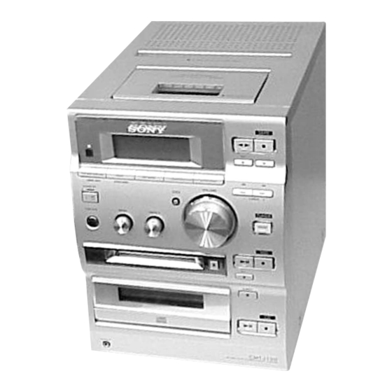
HCD-CP500K/CP500MD
SERVICE MANUAL
Ver 1.0 2001. 06
HCD-CP500K/CP500MD is the Amplifier,
MD deck, CD player, Tape player and Tuner
section in CMT-CP500K/CP500MD.
Amplifier section
For the U.S. model
AUDIO POWER SPECIFICATIONS
POWER OUTPUT AND TOTAL
HARMONIC DISTORTION:
With 6-ohm loads, both channels driven, from
70 - 20,000 Hz; rated 18 watts per channel
minimum RMS power, with no more than 0.9%
total harmonic distortion from 250 milliwatts to
rated output.
US, Canadian model:
Continuous RMS power output (reference):
Total harmonic distortion: less than 0.07% (6 ohms at
1 kHz, 18 W)
Sony Corporation
9-873-216-01
2001F1600-1
Home Audio Company
© 2001.6
Shinagawa Tec Service Manual Production Group
CD
Section
MD
Section
Tape deck
Section
SPECIFICATIONS
AEP, UK model:
DIN power output (rated): 30 + 30 W
Continuous RMS power output (reference):
Music power output (reference):
Other models:
The following measured at 230 V AC, 60 Hz
DIN power output (rated): 30 + 30 W
Continuous RMS power output (reference):
35 + 35 W
The following measured at 220 V AC, 60 Hz
(6 ohms at 1 kHz, 10%
DIN power output (rated): 24 + 24 W
THD)
Continuous RMS power output (reference):
MICRO HI-FI COMPONENT SYSTEM
Canadian Model
Australian Model
Model Name Using Similar Mechanism
CD Mechanism Type
Base Unit Type
Optical Pick-up Type
Model Name Using Similar Mechanism
MD Mechanism Type
Optical Pick-up Type
Model Name Using Similar Mechanism
Tape Transport Mechanism Type
(6 ohms at 1 kHz, DIN)
35 + 35 W
(6 ohms at 1 kHz, 10%
THD)
85 + 85 W
(6 ohms at 1 kHz, DIN)
35 + 35 W
(6 ohms at 1 kHz, 10%
THD)
(6 ohms at 1 kHz, DIN)
27 + 27 W
(6 ohms at 1 kHz, 10%
THD)
US Model
AEP Model
UK Model
E Model
Chinese Model
HCD-CP500MD
Korea Model
HCD-CP500K
New
CDM55F-K4BD43
BU-K4BD43
KSM-213DHAP
New
MDM-7B
KMS-260B
New
Mech deck
— Continued on next page —
Advertisement
Table of Contents

Related Manuals for Sony HCD-CP500MD


Summary of Contents for Sony HCD-CP500MD
- Page 1 Canadian Model Ver 1.0 2001. 06 AEP Model UK Model E Model Australian Model Chinese Model HCD-CP500MD Korea Model HCD-CP500K/CP500MD is the Amplifier, HCD-CP500K MD deck, CD player, Tape player and Tuner section in CMT-CP500K/CP500MD. Model Name Using Similar Mechanism...
- Page 2 Design and specifications are subject to change Recording system 4-track 2-channel stereo without notice. Frequency response 50 – 13,000 Hz (±3 dB), using a Sony TYPE I cassette ±0.15% W. Peak (IEC) Wow and flutter 0.1% W. RMS (NAB) ±0.2% W. Peak (DIN)
-
Page 3: Table Of Contents
···························· 26 refer to the following list. If any problem 6. ELECTRICAL ADJUSTMENTS ······························ 26 persists, consult your nearest Sony dealer. 7. DIAGRAMS 7-1. CIRCUIT BOARDS LOCATIONS ··································· 41 7-2. BLOCK DIAGRAM – CD SECTION – ··························· 42 BLOCK DIAGRAM – MAIN SECTION – ······················ 43 BLOCK DIAGRAM –... -
Page 4: Servicing Notes
DIAGRAMMES SCHÉMATIQUES ET LA LISTE DES PIÈCES SONT CRITIQUES POUR LA SÉCURITÉ DE FONCTIONNEMENT. NE REMPLACER CES COMPOSANTS QUE PAR DES PIÈSES SONY Notes on chip component replacement DONT LES NUMÉROS SONT DONNÉS DANS CE MANUEL OU • Never reuse a disconnected chip component. - Page 5 HCD-CP500K/CP500MD DRAWING OUT THE TRAY DURING POWER OUT Tray Move the cam block in the direction of the arrow with a finger. CLEANING THE OPTICAL PICK-UP (CD PLAYER) CD mechanism deck Floating screw Optical pick-up block Clean the lens block with applicator.
- Page 6 HCD-CP500K/CP500MD SERVICE POSITION OF THE MD MECHANISM DECK MD mechanism deck MAIN board (MDM-7B) CN304 MD DIGITAL board CN1001 BD board CN301 CN801 SERVICE POSITION OF THE CD MECHANISM DECK MAIN board CN308 LOADING board CD mechanism deck CN302 (CDM55F-K4BD43) CD board CN101...
- Page 7 HCD-CP500K/CP500MD SERVICE POSITION OF THE TAPE MECHANISM DECK Tape mechanism deck CN303 CN301...
- Page 8 HCD-CP500K/CP500MD JIG FOR CHECKING BD (MD) BOARD WAVEFORM The special jig (J-2501-196-A) is useful for checking the waveform of the BD (MD) board. The names of terminals and the checking items to be performed are shown as follows. GND : Ground I+3V : For measuring IOP (Check the deterioration of the optical pick-up laser) IOP : For measuring IOP (Check the deterioration of the optical pick-up laser) : TRK error signal (Traverse adjustment)
-
Page 9: General
HCD-CP500K/CP500MD SECTION 2 GENERAL BASS wd (40) PHONES jack wa TREBLE ws (40) CD EJECT Z qh (8, 9, 16, 50) PLAY MODE DIRECTION wj TUNER BAND qs (34, 35, 50) (9, 10, 13 – 15, 24, 37 – 39) CD x qj (9, 10, 17, 38) TUNING MODE wj (34, 35) PUSH OPEN/CLOSE Z 6 (37) -
Page 10: Setting The Time
HCD-CP500K/CP500MD Setting the time Turn on the system. Press CLOCK/TIMER SET on the remote. If you are setting the clock for the first time, go to step 5. Press . or > on the remote repeatedly until “CLOCK SET?” appears in the display. Press ENTER/YES on the remote. -
Page 11: Disassembly
HCD-CP500K/CP500MD SECTION 3 DISASSEMBLY • The equipment canbe removed using the following procedure. Upper cover and case (L), (R) (Page 11) Tape mechanism deck Front panel section Back panel and MAIN board (Page 12) (Page 12) (Page 14) CD mechanism deck Panel section MD mechanism POWER board... - Page 12 HCD-CP500K/CP500MD 3-2. TAPE MECHANISM DECK Top panel Tape mechanism deck 1 Flat cable 5 Four screws (12 core) (CN302) (+BTP 3 x 8) 3 Connector (CN301) 4 TC board 2 Three screws (+BVTT 2.6 x 5) 3-3. FRONT PANEL SECTION 3 Flat cable (25 core) (CN301) 1 Two screws...
- Page 13 HCD-CP500K/CP500MD 3-4. PANEL SECTION 4 Three screws (+BTP 3 x 8) 5 MD cover 6 Two screws (+BTP 3 x 8) qa MD-INDICATE board ql CONTROL board q; Screw (+BVTP 2.6 x 8) qj Eighteen screws 7 MD block (+BVTP 2.6 x 8) 8 Connector (CN806) qf CD-PRISM...
- Page 14 HCD-CP500K/CP500MD 3-5. BACK PANEL AND MAIN BOARD 5 Eight screws (+BTP 3 x 8) 2 Connector (CN551) qa OPTICAL board 0 Optical retainer board 9 Screw (+BTP 3 x 8) 1 Connector (CN902) 6 Back panel 7 Two screws (+BTP 3 x 12) 8 MAIN board 3 Connector (CN308)
- Page 15 HCD-CP500K/CP500MD 3-7. MD MECHANISM DECK SECTION 1 Flat cable (17 core) (CN103) 3 Two screws (+BTP 3 x 8) 2 Flat cable (27 core) 4 DIGITAL board (CN102) 6 MD cover 8 MD mechanism deck 7 MD cover 5 Two screws (+BTP 3 x 8) 3-8.
- Page 16 HCD-CP500K/CP500MD 3-9. BD BOARD Remove the solders (Two portion) Remove the solders (SLED motor) (Two portion) (SPINDLE motor) 6 Flexible board M102 (CN101) M101 Remove the solders (Two portion) M103 (LOADING motor) S102 Remove the solders (Three portion) 7 Connector (CN104) 5 Two screws 8 BD board (+BTP2 x 6)
- Page 17 HCD-CP500K/CP500MD 3-11. OVER WRITE HEAD (HR901) 1 Screw (P 1.7 x 6) 2 Over write head (HR901) 3-12. OPTICAL PICK-UP (MD) 8 Optical pick-up (for MD) 6 Main shaft 3 Screw (+BTP 2 x 6) 7 Flexible board 4 Base (BU-A) 5 Screw (+KTP2 x 6) 1 Screw (+BTP 2 x 6) 2 Base (BU-D)
- Page 18 HCD-CP500K/CP500MD 3-13. CD MECHANISM DECK SECTION 1 Two screws 2 MPEG braket (+BTP 3 x 8) 3 Screw (+BTP 3 x 8) 5 Connector (CN1) 6 CD mechanism deck (Two claws) 4 Flat cable (22core) (CN101) 3-14. TRY, GEAR AND D CAM SECTION (CDM55) 4 Belt (CDM55) 5 Spacer (55) 6 Pulley (LDG)
- Page 19 HCD-CP500K/CP500MD 3-15. CD BASE UNIT (CDM55) 2 Remove the HOLDER (BU) 1 Floating screw assembly in the direction (PTPWH M2.6) of the arrow A . 3 Chassis (F) 3-16. OPTICAL PICK-UP (CD) BLOCK SECTION (KSM-213DHAP) 2 Two screws (+PTPWH M2.6) qs Optical pick-up (CD) block (KSM-213DHAP) 8 Two insulators...
-
Page 20: Test Mode
HCD-CP500K/CP500MD SECTION 4 TEST MODE Note 1: About “R” As this unit has only a few buttons, some operations require the use of remote commander (RM-SCP500/provided with unit: 1-476-754-11) buttons. These operations are indicated as “R” in this manual. [MENU/NO] Example: ...Press the button of the remote commander. - Page 21 HCD-CP500K/CP500MD MD SECITON 1. PRECAUTIONS FOR USE OF TEST MODE • As operations related to loading will be performed regardless of the test mode operations being performed, be sure to check that the disc is stopped before setting and removing it. Even if the Z (MD) button is pressed while the disc is rotating during continuous playback, continuous recording, etc., the disc will not stop rotating.
- Page 22 HCD-CP500K/CP500MD 5. SELECTING THE TEST MODE There are 26 types of test modes as shown below. The groups can be switched by pressing the > button. After selecting the “R” “R” group to be used, press the ENTER/YES “R” button. After setting a certain group, pressing the >...
- Page 23 HCD-CP500K/CP500MD 5-1. Operating the Continuous Playback Mode 1. Entering the continuous playback mode (1) Set the disc in the unit. (Whichever recordable discs or discs for playback only are available) (2) Press the . “R” > “R” button to display “CPLAY 1MODE” (C34). (3) Press the ENTER/YES “R”...
- Page 24 HCD-CP500K/CP500MD 8. AUTOMATIC SELF-DIAGNOSIS FUNCTION This test mode performs CREC and CPLAY automatically for mainly checking the characteristics of the optical pick-up. To perform this test mode, the laser power must first be checked. Perform AUTO CHECK after the laser power check and Iop Compare. Procedure: Press the button to display “AUTO CHECK”...
- Page 25 HCD-CP500K/CP500MD 11. WHEN MEMORY NG IS DISPLAYED If the nonvolatile memory data is abnormal, “E001 MEMORY NG” will be displayed so that the MD deck does not continue operations. In this case, set the test mode promptly and perform the following procedure. Procedure: 1.
-
Page 26: Mechanical Adjustments
HCD-CP500K/CP500MD SECTION 5 SECTION 6 MECHANICAL ADJUSTMENTS ELECTRICAL ADJUSTMENTS Precaution DECK SECTION 0 dB=0.775V Clean the following parts with a denatured alcohol-moistened swab: Demagnetize the record/playback head with a head demagnetizer. record/playback heads pinch rollers Do not use a magnetized screwdriver for the adjustments. erase head rubber belts After the adjustments, apply suitable locking compound to the... - Page 27 HCD-CP500K/CP500MD Sample Value of Wow and flutter Mode: Playback W.RMS (JIS) less than 0.35% (test tape: WS-48B) test tape P-4-A100 SJ301 Record Level Check (10kHz, –10dB) SPEAKER Output Terminal oscilloscope Procedure: Press FUNCTION button to select ANALOG IN. (This step 6 Ω...
- Page 28 HCD-CP500K/CP500MD RF PLL Free-run Frequency CD SECTION Procedure : Note : 1. CD Block is basically designed to operate without adjustment. Connect frequency counter to TP (XPCK) with lead wire. Therefore, check each item in order given. 2. Use YEDS-18 disc (3-702-101-01) unless otherwise indicated. frequency counter CD BOARD 3.
- Page 29 HCD-CP500K/CP500MD MD SECTION Note 1:About “R” As this unit has only a few buttons, some operations require the use of remote commander (RM-SCP500/provided with unit: 1-476-754-11) buttons. These operations are indicated as “R” in this manual. [MENU/NO] Example: ...Press the button of the remote commander.
- Page 30 HCD-CP500K/CP500MD 2. PRECAUTIONS FOR CHECKING LASER DIODE 4. PRECAUTIONS FOR ADJUSTMENTS EMISSION 1. When replacing the following parts, perform the adjustments and checks with the mark in the order shown in the following To check the emission of the laser diode during adjustments, never table.
- Page 31 HCD-CP500K/CP500MD 5. USING THE CONTINUOUSLY RECORDED DISC Procedure: 1. Set the laser power meter on the objective lens of the optical * This disc is used in focus bias adjustment and error rate check. pick-up. (When it cannot be set properly, press the m “R”...
- Page 32 HCD-CP500K/CP500MD 6-4. Auto Check 6-6. Traverse Check This test mode performs CREC and CPLAY automatically for mainly checking the characteristics of the optical pick-up. To perform Note 1:Data will be erased during MO reading if a recorded disc is used in this adjustment. this test mode, the laser power must first be checked.
- Page 33 HCD-CP500K/CP500MD 6-7. Focus Bias Check 9. Press the ENTER/YES “R” button to display “EFB = P”. Change the focus bias and check the focus tolerance amount. Then, the optical pick-up moves to the pit area automatically Procedure: and servo is imposed. 1.
- Page 34 HCD-CP500K/CP500MD 7. INITIAL SETTING OF ADJUSTMENT VALUE Procedure: 1. Press the . “R” > “R” button to display “TEMP ADJUST” (C03). Note: Mode which sets the adjustment results recorded in the non-volatile 2. Press the ENTER/YES “R” button to select the “TEMP memory to the initial setting value.
- Page 35 HCD-CP500K/CP500MD 11. Iop NV SAVE 6. Press the . “R” > “R” button so that the reading of the laser power meter becomes the specified value, press the Write the reference values in the nonvolatile memory to perform ENTER/YES “R” button to save it.
- Page 36 HCD-CP500K/CP500MD 8. Press the . “R” > “R” button so that the waveform of 18. Press the ENTER/YES “R” button, display “EFB = SAVE” the oscilloscope becomes the specified value. for a moment and save the adjustment results in the non-volatile (When the .
- Page 37 HCD-CP500K/CP500MD 14. ERROR RATE CHECK 16. AUTO GAIN CONTROL OUTPUT LEVEL ADJUSTMENT 14-1. CD Error Rate Check Be sure to perform this adjustment when the optical pick-up is Procedure: replaced. 1. Load the check disc (TDYS-1). If the adjustment results becomes “Adjust NG!”, the optical pick- 2.
- Page 38 HCD-CP500K/CP500MD Adjustment and checking Loacation: – BD (MD) BOARD (Component Side) – – BD (MD) BOARD (Conductor Side) – D101 IC101 CN105 1. I+3V CN101 2. IOP 3. GND 4. TE 5. FE 6. VC 7. RF IC151 IC190 Note: It is useful to use the jig for checking the waveform. (Refer to Ser- vicing Notes on page 8)
- Page 39 HCD-CP500K/CP500MD MEMO...
-
Page 40: Diagrams
HCD-CP500K/CP500MD SECTION 7 DIAGRAMS 7-1. CIRCUIT BOARDS LOCATION TC board CONTROL board MD-INDICATE board CD-PRISM board MAIN board HEAD PHONE board POWER board OPTICAL board DIGITAL board BD board LOADING board CD board... -
Page 41: Circuit Boards Locations
HCD-CP500K/CP500MD • Waveforms THIS NOTE IS COMMON FOR PRINTED WIRING • Indication of transistor BOARDS AND SCHEMATIC DIAGRAMS. IC101 us XTAO IC1001 w; XOUT IC309 qf X-O (In addition to this, the necessary note is printed in each block.) 4.6 Vp-p 3.4 Vp-p 4 Vp-p These are omitted. -
Page 42: Block Diagram - Cd Section
HCD-CP500K/CP500MD 7-2. BLOCK DIAGRAM – CD SECTION – IC503 IC551 SELECTOR DIGITAL OPTICAL SECTION Q102 (Page 44) SWITCH IC101 OPTICAL PICK-UP DIGITAL SERVO, IC103 BLOCK DIGITAL SIGNAL PROCESSOR RF AMP D OUT RFAC RFAC RFDCO RFDC IC306(1/3) MASTER CONTROL CTRL1(1-2) Q101 XTSL XTSL... -
Page 43: Block Diagram - Main Section
HCD-CP500K/CP500MD BLOCK DIAGRAM – MAIN SECTION – MD-L • R-CH is omitted due to same as L-CH. SECTION IC301 • Signal Path (Page 44) SOUND PROCESSOR : FM LINEOUT1 REC-L : CD IC101 POWER AMP VOL1 29 : PB SJ301 OUT1 : REC Q101... -
Page 44: Block Diagram - Md Section
HCD-CP500K/CP500MD BLOCK DIAGRAM – MD SECTION – IC151 (1/2) IC181, Q181 182 EFMO ADDT OVER WRITE HEAD DRIVE DADTI FILI DADTI SAMPLING HR901 SCTX RATE XBCKI OVER WRITE HEAD XBCKI CONVERTER IC151 (1/2) CLTV LRCKI LRCKI DIGITAL SIGNAL PROCESSOR, EFM/ACIRC ENCODER/DECODER, FILO SHOCK PROOF MEMORY CONTROLLER, ATRAC ENCODER/DECODER... -
Page 45: Block Diagram - Panel Section
HCD-CP500K/CP500MD BLOCK DIAGRAM – PANEL SECTION – IC306(2/3) LCD801 MASTER CONTROL IC801 LIQUID CRYSTAL DISPLAY UNIT REMOTE SIRCS SENSOR XC-IN PC POWER J302 LCD-DATA X801 PC LINK Q302 32.768kHz XC-OUT I2C-CLK LCD-SCK SWITCH IIC-CLK S825 POWER KEY LCD-CS Q301 X-IN I2C-DATA X802 LCD-RS... -
Page 46: Printed Wiring Board - Cd Board
HCD-CP500K/CP500MD • See page 30 for Circuit Boards Location. 7-3. PRINTED WIRING BOARD – CD BOARD – S101 (LIMIT IN) IC702 (DVC1.65V) (TE) (XPCK) IC101 (RFAC) IC103 CN302 (Page 51) • Semiconductor Location Ref. No. Location D101 IC101 IC103 IC702 Q101 Q102 Q103... -
Page 47: Schematic Diagram - Cd Board
HCD-CP500K/CP500MD 7-4. SCHEMATIC DIAGRAM – CD BOARD – (Page 52) -
Page 48: Printed Wiring Board - Bd Board
HCD-CP500K/CP500MD • See page 30 for Circuit Boards Location. 7-5. PRINTED WIRING BOARD – BD BOARD – DIGITAL BOARD DIGITAL BOARD CN1003 CN1004 (Page 56) (Page 56) IC181 IC195 IC190 IC151 IC102 IC101 • Semiconductor • Semiconductor Location Location SIDE A SIDE B Ref. -
Page 49: Schematic Diagram - Bd Board (1/2)
HCD-CP500K/CP500MD 7-6. SCHEMATIC DIAGRAM – BD BOARD (1/2) – (Page 50) (Page 50) (Page 50) -
Page 50: Schematic Diagram - Bd Board (2/2)
HCD-CP500K/CP500MD 7-7. SCHEMATIC DIAGRAM – BD BOARD (2/2) – (Page 49) (Page 57) (Page 49) (Page 57) (Page 49) -
Page 51: Printed Wiring Boards - Audio Section
HCD-CP500K/CP500MD 7-8. PRINTED WIRING BOARDS – AUDIO SECTION – • See page 30 for Circuit Boards Location. CN801 (Page 58) (AEP,UK) (AEP,UK) IC306 (AEP,UK) IC309 IC307 CN304 (Page 58) IC302 CN1001 (Page 56) • Semiconductor Location CN551 (Page 58) Ref. No. Location Ref. -
Page 52: Schematic Diagram - Audio Section (1/2)
HCD-CP500K/CP500MD 7-9. SCHEMATIC DIAGRAM – AUDIO SECTION (1/2) – (Page 55) (Page 47) (Page 59) (Page 57) (Page 59) IC B/D (Page 53) -
Page 53: Schematic Diagram - Audio Section (2/2)
HCD-CP500K/CP500MD 7-10. SCHEMATIC DIAGRAM – AUDIO SECTION (2/2) – (Page 52) (Page 59) IC B/D IC B/D (Page 60) IC B/D IC B/D... -
Page 54: Printed Wiring Board - Tc Board
HCD-CP500K/CP500MD • See page 30 for Circuit Boards Location. 7-11. PRINTED WIRING BOARD – TC BOARD – CN303 (Page 51) IC401 IC402 • Semiconductor HEAD Location Ref. No. Location D401 IC401 IC402 Q401 Q402 Q403 Q406 Q407 Q413 Q414... -
Page 55: Schematic Diagram - Tc Board
HCD-CP500K/CP500MD 7-12. SCHEMATIC DIAGRAM – TC BOARD – IC B/D (Page 52) -
Page 56: Printed Wiring Board - Digital Board
HCD-CP500K/CP500MD • See page 30 for Circuit Boards Location. 7-13. PRINTED WIRING BOARD – DIGITAL BOARD – IC1006 IC1005 CN301 (Page 51) IC1001 IC1004 • Semiconductor Location CN103 CN102 Ref. No. Location (Page 48) (Page 48) IC1001 IC1004 IC1005 IC1006 Q1001 Q1002 Q1003... -
Page 57: Schematic Diagram - Digital Board
HCD-CP500K/CP500MD 7-14. SCHEMATIC DIAGRAM – DIGITAL BOARD – (Page 50) (Page 50) IC B/D IC B/D (Page 52) IC B/D... -
Page 58: Printed Wiring Boards - Control Section
HCD-CP500K/CP500MD • See page 30 for Circuit Boards Location. 7-15. PRINTED WIRING BOARDS – CONTROL SECTION – CN306 (Page 51) IC801 CN503 (Page 51) IC551 S801,802,804-806,809, 810,815,817-825 S803,811-814 • Semiconductor Location Ref. No. Location Ref. No. Location D801 D828 CN304 D802 (Page 51) D803... -
Page 59: Schematic Diagram - Control Board
HCD-CP500K/CP500MD 7-16. SCHEMATIC DIAGRAM – CONTROL SECTION – (Page 53) (Page 52) (Page 52) -
Page 60: Printed Wiring Board - Power Board
HCD-CP500K/CP500MD 7-17. PRINTED WIRING BOARD – POWER BOARD – 7-18. SCHEMATIC DIAGRAM – POWER BOARD – • See page 30 for Circuit Boards Location. CNP307 (Page 51) (EXCEPT CP500MD:E51,HK,TW) (EXCEPT CP500MD:E51,HK,TW) F905 (CP500MD:E51,HK,TW) (EXCEPT CP500MD:E51,HK,TW) (CP500MD:E51,HK,TW) S901 VOLTAGE SELECTOR 220V-240V 110V-120V (CP500MD:E51,HK,TW) •... -
Page 61: Ic Block Diagrams
HCD-CP500K/CP500MD 7-19. IC BLOCK DIAGRAMS IC101, 201 TDA7296 IC307 KA3082 THERMAL BIPOLAR SHUTDOWN DRIVER OUT TRANSCONDACTANCE INPUT STAGE MOS GAIN & SHORT – LEVEL SHIFTING OUTPUT CIRCUIT STAGE STAGE PROTECTION PRE DRIVER STANDBY/ MUTE LOGIC BOOST- SWITCH STRAP 8 9 10 14 15 IC309 BU1924F IC308 M62016L... - Page 62 HCD-CP500K/CP500MD IC1004 BA6209N FORWARD /REVERSE MOTOR MOTOR CONTROL DRIVE DRIVE 7 8 9 IC1005 µDA1360TS VDDA VSSA 14 FSEL VINL CLOCK – CONTROL VREF CANCELLATION DECIMATION FILTER FILTER 13 DATAO DIGITAL VINR – 12 WS INTERFACE 11 BCK VREF (N) VREF (P) 10 VSSD SFOR...
-
Page 63: Ic Pin Function Description
HCD-CP500K/CP500MD 7-20. IC PIN FUNCTION • IC101 CXA2523AR RF AMPLLFLER (BD BOARD) Pin No. Pin Name Description I-V converted RF signal I input I-V converted RF signal J input Middle point voltage (+1.5V) generation output 4 to 9 A to F Signal input from the optical pick-up detector Light amount monitor input Laser APC output... - Page 64 HCD-CP500K/CP500MD • IC151 CXD2662R DIGITAL SIGNAL PROCESSOR, DIGITAL SERVO SIGNAL PROCESSOR (BD BOARD) Pin No. Pin Name Description Function FOK signal output to the system control (monitor output) MNT0 (FOK) “H” is output when focus is on (Not used) MNT1 (SHCK) Track jump detection signal output to the system control (monitor output) MNT2 (XBUSY) Monitor 2 output to the system control (monitor output)
- Page 65 HCD-CP500K/CP500MD Pin No. Pin Name Description Data input/output for DRAM 50, 51 D2, D3 MVCI I (S) Clock input from an external VCO (Fixed at “L”) ASYO Playback EFM duplex signal output ASYI I (A) Playback EFM comparator slice level input AVDD —...
- Page 66 HCD-CP500K/CP500MD Pin No. Pin Name Description TFDR Tracking servo drive PWM output (+) DVDD — +3V power supply (Digital) FFDR Focus servo drive PWM output (+) FRDR Focus servo drive PWM output (–) 176.4 kHz clock signal output (X’tal) (Not used) SRDR Sled servo drive PWM output (–) SFDR...
- Page 67 HCD-CP500K/CP500MD • IC306 M30622MGA-A44FP MASTER CONTROL (MAIN BOARD) Pin No. Pin Name Description AC-CUT AC CUT ON/OFF check signal input (L=ON,H=OFF) POWER-ON Power relay ON/OFF signal output (H=ON,L=OFF) XTSL XTSL signal output for IC101 SIRCS Remote control receiver data signal input DA_MUTE D/A (MD) muting control signal output SOL_CON...
- Page 68 HCD-CP500K/CP500MD Pin No. Pin Name Description H/P_CHECK Headphone detect signal input H/P_MUTE Headphone muting control signal output AMP_MUTE Power amplifier muting control signal output (L=ON,H=OFF) VOL_CLK Volume clock signal output VOL_DATA Volume data signal output STK_POWER Power amplifier ON/OFF signal output (H=ON,L=OFF) LINE-MUTE Line muting control signal output (H=ON,L=OFF) —...
- Page 69 HCD-CP500K/CP500MD • IC1001 M30805MG-205GP SYSTEM CONTROL (DIGITAL BOARD) Pin No. Pin Name Description — — Not used — — Not used LVLI — Not used LVL0 — Not used (TXD3) — Not used (RXD3) — Not used (CLK3) — Not used MUTE Line out muting output L: Muting DARST...
- Page 70 HCD-CP500K/CP500MD Pin No. Pin Name Description — — Not used — — Not used — — Not used — Not used MNT2 (XBUSY) In the state of executive command from the CXD2662R VSS2 — Ground MNT1 (SHCK) Track jump signal input from the CXD2662R VCC2 —...
-
Page 71: Exploded Views
HCD-CP500K/CP500MD SECTION 8 EXPLODED VIEWS NOTE: • -XX, -X mean standardized parts, so they may • Abbreviation The components identified by mark ! or have some differences from the original one. : Australian model dotted line with mark ! are critical for safety. •... - Page 72 HCD-CP500K/CP500MD 8-2. FRONT PANEL SECTION LCD801 not supplied supplied Supplied with RV801 Ref. No. Part No. Description Remarks Ref. No. Part No. Description Remarks 4-232-471-01 WINDOW, CD 4-217-319-21 PLATE, LCD LIGHT 4-232-441-01 KNOB (VOL) 4-234-566-01 LCD SHIEET 4-234-573-01 KNOB (TIBASS) A-2056-914-A MD-INDICATE BOARD, COMPLETE 4-234-562-01 WINDOW (LCD) A-2056-914-A CD-PRISM BOARD, COMPLETE...
-
Page 73: Chassis Section
HCD-CP500K/CP500MD 8-3. CHASSIS SECTION not supplied not supplied T902 CDM55F-K4BD43 not supplied not supplied not supplied Ref. No. Part No. Description Remarks Ref. No. Part No. Description Remarks 4-232-434-01 LID, CD 1-757-943-11 WIRE (FLAT TYPE) (22CORE) 4-234-551-01 BRACKET,MPEG 4-217-354-11 BUSHING, INSULATING A-4725-836-A POWER BOARD, COMPLETE A-4725-837-A MAIN BOARD, COMPLETE (CP500MD:AEP,UK) (CP500K/CP500MD:AEP,UK,AUS,CH,TH) - Page 74 HCD-CP500K/CP500MD 8-4. MD MECHANISM DECK SECTION-1 (MDM-7B) not supplied supplied not supplied Ref. No. Part No. Description Remarks Ref. No. Part No. Description Remarks ∗ 151 4-996-267-01 BASE (BU-D) 4-227-012-01 SPRING (HOLDER), TENSION 4-231-319-01 SCREW (+BTP) (2X6) A-4680-638-B PLATE (HOLDER) ASSY, RETAINER 4-226-994-01 GUIDE (L) 4-226-995-01 SLIDER (EJ) A-4735-075-A HOLDER ASSY...
- Page 75 HCD-CP500K/CP500MD 8-5. MD MECHANISM DECK SECTION-2 (MDM-7B) HR901 S102 M101 M102 M103 Ref. No. Part No. Description Remarks Ref. No. Part No. Description Remarks 4-231-319-01 SCREW (+BTP) (2X6) 4-226-992-01 BASE, SL 3-372-761-01 SCREW (M1.7), TAPPING 4-227-023-01 SPRING (SPINDLE), TORSION 4-227-008-01 GEAR (SC) 4-227-004-01 GEAR (LC) 4-227-009-01 GEAR (SD) 4-227-005-01 GEAR (LD)
- Page 76 HCD-CP500K/CP500MD 8-6. CD MECHANISM DECK SECTION-1 (CDM55F-K4BD43) M901 not supplied BU-K4BD43 Ref. No. Part No. Description Remarks Ref. No. Part No. Description Remarks 4-925-315-31 DAMPER 4-220-234-01 PULEY (LDG) 4-224-894-01 TRAY 4-220-237-01 GEAR (A) 1-676-599-11 LOADING BOARD 4-221-815-01 ROLLER 4-220-229-01 LEVER (SW) 4-231-779-01 CHASSIS (F) 4-220-239-01 SPRING,TORSION A-4735-082-A MAGNET ASSY...
-
Page 77: Cd Mechanism Deck Section
HCD-CP500K/CP500MD 8-7. CD MECHANISM DECK SECTION-2 (BU-K4BD43) Ref. No. Part No. Description Remarks Ref. No. Part No. Description Remarks 4-221-817-02 SHAFT (BU) 1-757-055-11 WIRE (FLAT TYPE) (16 CORE) 4-231-780-01 HOLDER (BU) 4-229-005-01 INSULATOR (213) 4-229-004-01 SPRING (213), COMPRESSION 4-985-672-01 SCREW (+PTPWHM2.6), FLOATING A-4476-973-A CD BOARD, COMPLETE 0 308 A-4735-357-A BASE ASSY, OP (KSM-213DHAP/Z-NP) -
Page 78: Electrical Parts List
HCD-CP500K/CP500MD SECTION 9 ELECTRICAL PARTS LIST NOTE: • Due to standardization, replacements in the • COILS uH: µH When indicating parts by reference number, parts list may be different from the parts please include the board name. specified in the diagrams or the components •... - Page 79 HCD-CP500K/CP500MD Ref. No. Part No. Description Remarks Ref. No. Part No. Description Remarks IC181 8-759-481-17 IC MC74ACT08DTR2 R111 1-216-833-11 METAL CHIP 1/16W IC190 8-759-677-64 IC L88M35T R112 1-216-829-11 METAL CHIP 4.7K 1/16W IC195 8-759-640-41 IC BR24C08F-E2 R113 1-216-833-11 METAL CHIP 1/16W R114 1-216-827-11 METAL CHIP...
- Page 80 HCD-CP500K/CP500MD Ref. No. Part No. Description Remarks Ref. No. Part No. Description Remarks < VIBRATOR > C245 1-126-204-11 ELECT CHIP 47uF C247 1-164-227-11 CERAMIC CHIP 0.022uF X171 1-781-569-21 OSCILLATOR, CRYSTAL (90MHz) C248 1-164-227-11 CERAMIC CHIP 0.022uF ∗∗∗∗∗∗∗∗∗∗∗∗∗∗∗∗∗∗∗∗∗∗∗∗∗∗∗∗∗∗∗∗∗∗∗∗∗∗∗∗∗∗∗∗∗∗∗∗∗∗∗∗∗∗∗∗∗∗∗∗ C249 1-164-360-11 CERAMIC CHIP 0.1uF A-4476-973-A CD BOARD, COMPLETE <...
- Page 81 HCD-CP500K/CP500MD CD-PRISM CONTROL Ref. No. Part No. Description Remarks Ref. No. Part No. Description Remarks R212 1-216-813-11 METAL CHIP 1/16W < CAPACITOR > R213 1-216-864-11 METAL CHIP 1/16W R214 1-216-864-11 METAL CHIP 1/16W C841 1-124-259-11 ELECT 4.7uF 20.00% 16V R215 1-216-864-11 METAL CHIP 1/16W C842...
- Page 82 HCD-CP500K/CP500MD CONTROL DIGITAL Ref. No. Part No. Description Remarks Ref. No. Part No. Description Remarks R808 1-216-819-11 METAL CHIP 1/16W S813 1-571-760-11 SWITCH, KEY BOARD (REPEAT) R809 1-216-820-11 METAL CHIP 1/16W S814 1-571-760-11 SWITCH, KEY BOARD R810 1-216-822-11 METAL CHIP 1.2K 1/16W (PLAY MODE/DIRECTION)
- Page 83 HCD-CP500K/CP500MD DIGITAL HEAD PHONE Ref. No. Part No. Description Remarks Ref. No. Part No. Description Remarks C1048 1-126-933-11 ELECT 100uF 20.00% 16V R1067 1-216-833-11 METAL CHIP 1/16W C1049 1-162-974-11 CERAMIC CHIP 0.01uF R1068 1-216-833-11 METAL CHIP 1/16W C1050 1-162-974-11 CERAMIC CHIP 0.01uF R1073 1-216-073-00 RES-CHIP...
- Page 84 HCD-CP500K/CP500MD HEAD PHONE LOADING MAIN Ref. No. Part No. Description Remarks Ref. No. Part No. Description Remarks < RESISTOR > C107 1-115-467-11 CERAMIC CHIP 0.22uF 10.00% 10V (CP500MD:E51,HK) R128 1-216-801-11 METAL CHIP 1/16W C108 1-115-467-11 CERAMIC CHIP 0.22uF 10.00% 10V R139 1-216-829-11 METAL CHIP 4.7K...
- Page 85 HCD-CP500K/CP500MD MAIN Ref. No. Part No. Description Remarks Ref. No. Part No. Description Remarks C206 1-104-664-11 ELECT 47uF 20.00% 16V C305 1-104-664-11 ELECT 47uF 20.00% 16V (CP500MD:AEP,UK) (CP500MD:AEP,UK) C206 1-126-963-11 ELECT 4.7uF 20.00% 50V C306 1-126-964-11 ELECT 10uF 20.00% 50V (CP500MD:E51,HK) (EXCEPT CP500MD:AEP,UK,E51,HK) C207...
- Page 86 HCD-CP500K/CP500MD MAIN Ref. No. Part No. Description Remarks Ref. No. Part No. Description Remarks C348 1-107-826-11 CERAMIC CHIP 0.1uF 10.00% 16V < CONNECTOR > C349 1-107-826-11 CERAMIC CHIP 0.1uF 10.00% 16V C350 1-124-903-11 ELECT 20.00% 50V CN301 1-794-470-11 CONNECTOR, FFC/FPC 25P C351 1-107-826-11 CERAMIC CHIP 0.1uF...
- Page 87 HCD-CP500K/CP500MD MAIN Ref. No. Part No. Description Remarks Ref. No. Part No. Description Remarks FB322 1-410-993-11 INDUCTOR CHIP 1uH Q319 8-729-034-51 TRANSISTOR KTC3875 FB323 1-216-864-11 METAL CHIP 1/16W Q320 8-729-202-56 TRANSISTOR 2SA950-Y-TPE2 FB324 1-216-864-11 METAL CHIP 1/16W Q321 8-729-055-94 TRANSISTOR SRC1202S FB325 1-216-864-11 METAL CHIP...
- Page 88 HCD-CP500K/CP500MD MAIN Ref. No. Part No. Description Remarks Ref. No. Part No. Description Remarks R133 1-216-833-11 METAL CHIP 1/16W R234 1-218-272-11 RES-CHIP 5.1K 1/16W (CP500MD:AEP,UK,E51,HK) (CP500MD:E51,HK) R134 1-216-829-11 METAL CHIP 4.7K 1/16W R235 1-216-825-11 METAL CHIP 2.2K 1/16W (EXCEPT CP500MD:AEP,UK,E51,HK) R236 1-216-833-11 METAL CHIP 1/16W...
- Page 89 HCD-CP500K/CP500MD MAIN Ref. No. Part No. Description Remarks Ref. No. Part No. Description Remarks R355 1-216-821-11 METAL CHIP 1/16W R439 1-216-821-11 METAL CHIP 1/16W R356 1-216-821-11 METAL CHIP 1/16W R440 1-216-821-11 METAL CHIP 1/16W R357 1-216-821-11 METAL CHIP 1/16W R441 1-216-821-11 METAL CHIP 1/16W R358...
- Page 90 HCD-CP500K/CP500MD MAIN MD-INDICATE OPTICAL POWER Ref. No. Part No. Description Remarks Ref. No. Part No. Description Remarks < VIBRATOR > A-4725-836-A POWER BOARD, COMPLETE (CP500K/CP500MD:AEP,UK,AUS,CH,TH) X301 1-579-242-41 VIBRATOR, CRYSTAL (4.332Hz) A-4725-843-A POWER BOARD, COMPLETE (CP500MD:AEP,UK) (CP500MD:US,CND) X801 1-567-098-41 VIBRATOR, CRYSTAL (32.768MHz) A-4725-850-A POWER BOARD, COMPLETE X802 1-781-107-21 VIBRATOR, SERAMIC (10MHz)
- Page 91 HCD-CP500K/CP500MD POWER Ref. No. Part No. Description Remarks Ref. No. Part No. Description Remarks D919 8-719-991-33 DIODE 1SS133T-77 < TRANSFORMER > D920 8-719-991-33 DIODE 1SS133T-77 0 T901 1-437-251-11 TRANSFORMER, POWER < FUSE > (CP500K/CP500MD:AEP,UK,AUS,CH,TH) 0 T901 1-437-253-11 TRANSFORMER, POWER 0 F901 1-533-466-11 FUSE, GLASS TUBE (DIA.
- Page 92 HCD-CP500K/CP500MD Ref. No. Part No. Description Remarks Ref. No. Part No. Description Remarks < IC > R442 1-216-825-11 METAL CHIP 2.2K 1/16W IC401 8-759-242-58 IC TA8189N < TRANSFORMER > IC402 8-759-508-69 IC BA3126N T401 1-433-372-11 TRANSFORMER, BIAS OSCILLATION < TRANSISTOR > T402 1-419-080-11 COIL T403...
- Page 93 HCD-CP500K/CP500MD MEMO...
- Page 94 HCD-CP500K/CP500MD REVISION HISTORY Clicking the version allows you to jump to the revised page. Also, clicking the version at the upper right on the revised page allows you to jump to the next revised page. Ver. Date Description of Revision 2001.06...
Need help?
Do you have a question about the HCD-CP500MD and is the answer not in the manual?
Questions and answers
How do I fix mini disc ejection failure
To fix MiniDisc ejection failure on the Sony HCD-CP500MD, you should check and possibly replace the loading mechanism belt. This belt is a common failure point in similar Sony MiniDisc decks. Replacing it with a compatible new belt can restore proper disc load/eject functions. Make sure to open the cassette door before reassembling the top panel to avoid damaging the mechanism. After replacement, test the unit to confirm the mechanism opens and closes correctly.
This answer is automatically generated
Il cd nn esce
The CD is not ejecting from the Sony HCD-CP500MD likely due to a faulty or worn drive belt in the loading mechanism. This issue can prevent the tray from opening or moving properly, and accessing it may require disassembling the unit to reach and replace the belt.
This answer is automatically generated