Table of Contents
Advertisement
Quick Links
SERVICE MANUAL
Ver 1.1 2003. 05
HCD-CP505 is the Amplifier, CD player, MD
deck, Tape player and Tuner section in
CMT-CP505MD.
Amplifier section
European model:
DIN power output (rated): 30 + 30 W
(6 ohms at 1 kHz, DIN)
Continuous RMS power output (reference):
35 + 35 W
(6 ohms at 1 kHz, 10%
THD)
Music power output (reference):
70 + 70 W
Other models:
The following measured at 230 V AC, 60 Hz
DIN power output (rated): 25 + 25 W
(6 ohms at 1 kHz, DIN)
Continuous RMS power output (reference):
30 + 30 W
(6 ohms at 1 kHz, 10%
THD)
The following measured at 220 V AC, 60 Hz
DIN power output (rated): 22 + 22 W
(6 ohms at 1 kHz, DIN)
Continuous RMS power output (reference):
28 + 28 W
(6 ohms at 1 kHz, 10%
THD)
Sony Corporation
9-874-070-02
Home Audio Company
2003E16-1
Published by Sony Engineering Corporation
© 2003.05
HCD-CP505
Model Name Using Similar Mechanism
CD
CD Mechanism Type
Section
Base Unit Type
Optical Pick-up Type
Model Name Using Similar Mechanism
MD
MD Mechanism Type
Section
Optical Pick-up Type
Tape deck
Model Name Using Similar Mechanism
Section
Tape Transport Mechanism Type
SPECIFICATIONS
Inputs
ANALOG IN:
Sensitivity 250 mV,
(phono jacks)
impedance 47 kilohms
DIGITAL OPTICAL IN (supported sampling
frequencies: 32 kHz, 44.1 kHz and 48 kHz)
Outputs
PHONES:
Accepts headphones with
an impedance of 8 ohms
or more
SPEAKER:
accepts impedance of 6 to
16 ohms.
CD player section
System
Compact disc and digital
audio system
Laser
Semiconductor laser
(λ=780 nm)
Emission duration:
continuous
Frequency response
2 Hz – 20 kHz
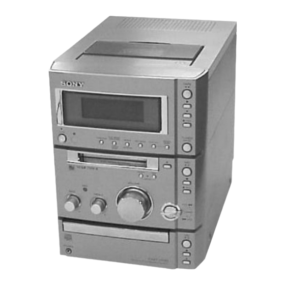
MICRO HI-FI COMPONENT SYSTEM
AEP Model
UK Model
E Model
Chinese Model
NEW
CDM55G-30BBD61B
BU-30BBD61B
A-MAX. 3
NEW
MDM-7S2C
KMS-262E
NEW
CMAL1Z-221A
MD deck section
System
Minidisc digital audio
system
Laser
Semiconductor laser
(λ=780 nm)
Emission duration:
continuous
Sampling frequency
44.1 kHz
Frequency response
5 Hz – 20 kHz
Tape deck section
Recording system
4-track 2-channel stereo
Frequency response
50 – 13,000 Hz (±3 dB),
using Sony TYPE I
cassettes
— Continued on next page —
Advertisement
Table of Contents

Related Manuals for Sony HCD-CP505


Summary of Contents for Sony HCD-CP505
- Page 1 HCD-CP505 SERVICE MANUAL AEP Model UK Model Ver 1.1 2003. 05 E Model Chinese Model HCD-CP505 is the Amplifier, CD player, MD deck, Tape player and Tuner section in CMT-CP505MD. Model Name Using Similar Mechanism CD Mechanism Type CDM55G-30BBD61B Section...
- Page 2 Intermediate frequency 10.7 MHz selector FM lead antenna (1) AM tuner section Power consumption Optional accessories Sony PC connection kit Tuning range European model: See the name plate (See the catalogue and European model: 531 - 1,602 kHz 0.3 watts (at the Power...
-
Page 3: Table Of Contents
LIST ARE CRITICAL TO SAFE OPERATION. REPLACE THESE Ordinary soldering irons can be used but the iron tip has to be COMPONENTS WITH SONY PARTS WHOSE PART NUMBERS applied to the solder joint for a slightly longer time. APPEAR AS SHOWN IN THIS MANUAL OR IN SUPPLEMENTS Soldering irons using a temperature regulator should be set to PUBLISHED BY SONY. - Page 4 No component is connected to the DIGITAL the problem refer to the following list. If any OPTICAL IN jack, or you tried to record from the problem persists, consult your nearest Sony digital component which is not connected dealer. correctly.
- Page 5 HCD-CP505 Messages Incomplete! Adjustment of the recording level after recording One of the following messages may appear or or Fade-in and Fade-out procedures have failed flash in the display during operation. since the system was either subject to vibration or there is a damaged or dirty disc in the tray.
- Page 6 HCD-CP505 Self-diagnosis display (continued) No Disc There is no CD in the player. Smart Space OVER The signal was input again after silence continued You have reached the end of the CD while turning for 3 or more but less than 30 seconds during...
- Page 7 HCD-CP505 Note 1: About “R” As this unit has only a few buttons, some operations require the use of remote commander (RM-SCP500/provided with unit) buttons. These operations are indicated as “R” in this manual. Example: MENU/NO “R” ...Press the MENU/NO button of the remote commander.
- Page 8 HCD-CP505 Items of Error History Mode Items and Contents Selecting the Test Mode Display History op rec tm Displays the accumulated recording time. When the accumulated recording time is more than 1 minute, displays the hour and minute When less than 1 minute, displays “Under 1 min”...
- Page 9 HCD-CP505 Table of Error Codes Error Code Description Could not perform loading The changer error occurred Loading switches combined incorrectly Timed out without reading the top of PTOC Could read top of PTOC, but detected error Timed out without accessing UTOC...
-
Page 10: Servicing Notes
HCD-CP505 SECTION 1 SERVICING NOTE Jig For Checking BD (MD) Board Waveform The special jig (J-2501-196-A) is useful for checking the waveform of the BD board. The names of terminals and the checking items to be performed are shown as follows. - Page 11 HCD-CP505 Iop DATA RECORDING AND DISPLAY WHEN OPTICAL PICK-UP AND NON-VOLATILE MEMORY (IC195 OF BD BOARD) ARE REPLACED The Iop value labeled on the optical pick-up can be stored in the non-volatile memory. By storing the value, it will eliminate the need to look at the value on the label of the optical pick-up.
-
Page 12: General
HCD-CP505 SECTION 2 This section is extracted GENERAL from instruction manual. Main unit BUTTON DESCRIPTIONS ALPHABETICAL ORDER ?/1 (power) e; A – G M – V m/M ql BASS wh (47) MD slot wk (13) l/L ql CD NX qh (9, 10, 22) -
Page 13: Remote Control
HCD-CP505 Remote Control BUTTON DESCRIPTIONS ALPHABETICAL ORDER @/1 (power) 1 A – F M – V BASS/TRE 4 (47) MD wf (15, 24, 25, 28, 29, 31– X qf 37, 39, 40) x qa CD wd (10–13) MENU/NO qg (12, 13, 23–26,... -
Page 14: Setting The Clock
HCD-CP505 Setting the clock Press ?/1 to turn on the system. Press CLOCK/TIMER SET on the remote. Press . or > on the remote repeatedly to set the hour. Press ENTER/YES or CURSORt on the remote. Press . or > on the remote repeatedly to set the minute. -
Page 15: Disassembly
HCD-CP505 SECTION 3 DISASSEMBLY • The equipment can be removed using the following procedure. TOP PANEL SECTION BACK PANEL SECTION FRONT PANEL, CASSETTE MECHANISM DECK MD MECHANISM DECK BLOCK (INCLUDING OPTICAL BOARD, OPTICAL RETAINER BOARD) MD MECHANISM DECK SWITCH BOARD, JACK BOARD... -
Page 16: Top Panel Section
HCD-CP505 Note: Follow the disassembly procedure in the numerical order given. 3-1. Top Panel Section 0 Remove the top cover in the 7 two screws direction of the arrow. (BTP 3 × 8) 2 screw (BTP 3 × 8) 3 Remove the panel side (L) in the direction of the arrow. -
Page 17: Front Panel, Md Mechanism Deck Block
HCD-CP505 3-3. Front Panel, MD Mechanism Deck Block 1 two screws (BVTP 3 × 8) 5 MD mechanism deck block 2 screw (BVTP 3 × 8) 3 screw (BVTP 3 × 8) 4 wire (flat type) (27 core) (CN608 ) -
Page 18: Switch Board, Jack Board
HCD-CP505 3-4. SWITCH Board, JACK Board 3 two bass knobs 1 volume knob 2 tuning knob front panel 8 SWITCH board 6 seventeen screws (BVTP 2.6 × 8) 5 JACK board 4 three screws 7 wire (flat type) (27 core) (BVTP 2.6 ×... -
Page 19: Back Panel Section (Including Optical Board, Optical Retainer Board)
HCD-CP505 3-5. Back Panel Section (Including OPTICAL Board, OPTICAL RETAINER Board) 7 OPTICAL board 0 back panel 6 OPTICAL RETAINER board 5 two screws (BVTP 3 × 8) 3 four screws (BTP 3 × 8) 1 connector cable (CN602 ) 4 three screws (BTP 3 ×... -
Page 20: Power Board
HCD-CP505 3-7. POWER Board 1 connector cable 6 POWER board (CN901 ) 4 POWER RETAINER board 5 four screws (BVTT 4 × 8) 3 screw (BVTP 3 × 8) 2 cord stopper 3-8. CONTROL Board, CD Mechanism Deck (CDM55G-30BBD61B) 2 two screws (BVTP 3 ×... -
Page 21: Cam (Cdm55)
HCD-CP505 3-9. Cam (CDM55) 4 belt (CDM55) 5 spacer (55) 6 pulley (LDG) 8 gear (B) 9 gear (A) 7 roller q; cam (CDM55) 2 Push the claw in the direction of the arrow C . 1 Pull out the tray in the direction of the arrow A . -
Page 22: Optical Pick-Up (Bu-30B Assy)
HCD-CP505 3-11. Optical Pick-Up (BU-30B Assy) 4 two floating screws qd BU-30B assy (+PTPWH M2.6) 9 two insulators 8 two insulators qa Remove the two solderings 0 Remove the two solderings qs BD (CD) board 1 wire (flat type) (16 core) -
Page 23: Digital Board
HCD-CP505 3-13. DIGITAL Board 5 MD cover (lower) 2 two screws (BVTP 3 × 8) 3 two screws (BVTP 3 × 8) 4 lead (with connector) 1 wire (flat type) (25 core) 6 three screws (BVTP 3 × 8) 7 DIGITAL board 8 MD bracket 3-14. -
Page 24: Bd (Md) Board
HCD-CP505 3-15. BD (MD) Board 1 Remove the two solderings (sled motor) 2 Remove the two solderings (spindle motor) M102 6 flexible board (CN101) M101 3 Remove the M103 two solderings (loading motor) S102 4 Remove the three solderings 8 BD (MD) board... -
Page 25: Over Wright Head (Hr901)
HCD-CP505 3-17. Over Wright Head (HR901) 1 screw (P 1.7 × 6) 2 over write head (HR901) 3-18. Mini Disc Device (KMS-262E) 8 Mini disc device (KMS-262E) 6 main shaft 3 screw (+B (P) TRI 2 × 6 CZN) 4 base (BU-A) -
Page 26: Test Mode
HCD-CP505 SECTION 4 TEST MODE Note 1: About “R” As this unit has only a few buttons, some operations require the use of remote commander (RM-SCP500/provided with unit) buttons. These operations are indicated as “R” in this manual. Example: MENU/NO “R” ...Press the MENU/NO button of the remote commander. - Page 27 HCD-CP505 8. To exit from this mode, press ?/1 button or disconnect the power cord. 4. CD Ship Mode (Setting the Position for Transportation) Press ?/1 button to turn the power on. Press FUNCTION to change the function to “CD”.
- Page 28 HCD-CP505 MD TEST MODE 1. Precautions For Use of Test Mode • As operations related to loading will be performed regardless of the test mode operations being performed, be sure to check that the disc is stopped before setting and removing it.
- Page 29 HCD-CP505 Group Display Details Mark Check Service AUTO CHECK Automatic self-diagnosis Err Display Error history display, clear TEMP ADJUST Temperature compensation offset adjustment LDPWR ADJUST Laser power adjustment Iop Write Iop data writing Iop NV Save Writes current Iop value in read nonvolatile memory using microprocessor...
- Page 30 HCD-CP505 5-2. Operating the Continuous Recording Mode (Use only when performing self-recording/playback check) Entering the continuous recording mode (1) Set a recordable disc in the unit. (2) Press the . “R” or > “R” button to display “CRE 2MODE” (C37) (3) Press the ENTER/YES “R”...
-
Page 31: Electrical Adjustments
HCD-CP505 SECTION 5 ELECTRICAL ADJUSTMENTS MD SECTION Note 1:About “R” As this unit has only a few buttons, some operations require the use of remote commander (RM-SCP500/provided with unit) buttons. These operations are indicated as “R” in this manual. Example: MENU/NO “R” ...Press the MENU/NO button of the remote commander. - Page 32 HCD-CP505 Flow Chart for Adjustment Start After turning the power off and on, initialises the non-volatile IC195 replacement memory (EEPROM). 7. Initial setting of adjustment value (See page 37) OP or IC195 replacement IC101, IC195 or D101 9. Temperature compensation offset adjustment (See page 37)
- Page 33 HCD-CP505 Precautions for Checking Laser Diode 5. When observing several signals on the oscilloscope, etc., make sure that VC and ground do not connect inside the Emission oscilloscope. To check the emission of the laser diode during adjustments, never (VC and ground will become short-circuited.) view directly from the top as this may lose your eye-sight.
- Page 34 HCD-CP505 Using the Continuously Recorded Disc Procedure: Set the laser power meter on the objective lens of the optical * This disc is used in focus bias adjustment and error rate check. pick-up. (When it cannot be set properly, press the m but- The following describes how to create a continuous recording ton or M button to move the optical pick-up.)
- Page 35 HCD-CP505 6-4. Auto Check 6-6. Traverse Check This test mode performs CREC and CPLAY automatically for mainly checking the characteristics of the optical pick-up. To Note 1: Data will be erased during MO reading if a recorded disc is used in this adjustment.
- Page 36 HCD-CP505 6-7. Focus Bias Check 9. Press the ENTER/YES “R” button to display “EFB = Change the focus bias and check the focus tolerance amount. MO-P”. Procedure: Then, the optical pick-up moves to the pit area automatically 1. Load the test disc (MDW-74/GA-1).
- Page 37 HCD-CP505 Initial Setting of Adjustment Value 5. When the ENTER/YES “R” button is pressed, “TEMP = SAVE” will be displayed and turned back to “TEMP ADJUST” Note: Mode which sets the adjustment results recorded in the non-volatile (C03) display then.
- Page 38 HCD-CP505 6. Press the “R” or “R” button so that the reading of > After the display changes to “Iop = save?”, press the laser power meter becomes the specified value, press the ENTER/YES “R” button. the ENTER/YES “R” button to save it.
- Page 39 HCD-CP505 8. Press the “R” or “R” button so that the waveform 19. Press the Z (MD) button and take out the check disc. > of the oscilloscope becomes the specified value. Adjustment Location: BD (MD) board (see page 41) (When the “R”...
- Page 40 HCD-CP505 14. Error Rate Check 16. Auto Gain Control Output Level Adjustment Be sure to perform this adjustment when the optical pick-up is 14-1. CD Error Rate Check replaced. Procedure: If the adjustment results becomes “Adjust NG!”, the optical pick- 1.
- Page 41 HCD-CP505 Adjustment and checking Loacation: – BD (MD) BOARD (Side A) – – BD (MD) BOARD (Side B) – D101 CN101 IC101 CN105 IC701 IC201 IC933 IC195 CN103 CN102...
- Page 42 HCD-CP505 Mode: Playback DECK SECTION 0 dB=0.775V Demagnetize the record/playback head with a head demagnetizer. test tape Do not use a magnetized screwdriver for the adjustments. P-4-A100 SJ301 (10kHz, –10dB) SPEAKER After the adjustments, apply suitable locking compound to the...
- Page 43 HCD-CP505 Mode: Record E-F Balance (1 Track jump) Check ANALOG IN (SJ302) Oscilloscope 1) 60 Hz BD (CD) BOARD 109 mV (–17 dB) 2) 5 kHz 3) 10 kHz AF OSC TP (TE) blank tape TP (DVC 1.65V) 600 Ω...
-
Page 44: Diagrams
HCD-CP505 SECTION 6 DIAGRAMS THIS NOTE IS COMMON FOR PRINTED WIRING • Abbreviation CH : Chinese model BOARDS AND SCHEMATIC DIAGRAMS. HK : Hong Kong model (In addition to this, the necessary note is printed • Signal path. in each block.) -
Page 45: Circuit Boards Location
HCD-CP505 6-1. Circuit Boards Location • Waveforms OPTICAL board – BD (CD) Board – – BD (MD) Board – – CONTROL Board – IC103 qg (RFAC) IC101 ek (RF) IC306 qa (XCOUT) TC board (PLAY mode) (PLAY mode) 3.6 Vp-p SWITCH board 30.5 µ... -
Page 46: Block Diagrams
HCD-CP505 6-2. Block Diagrams MD Section MAIN CD IN SECTION IC1008 IC1008 IC601 DIGITAL IC1008 OPTICAL IC1008 DIGITAL SERVO DIGITAL SIGNAL PROC. A/D CONV IC201 IC201 REC L IN IC181 DATAI DATAO VIN L Q181,182 HR901 OVER WRITE OVER WRITE... -
Page 47: Cd And Main Section
HCD-CP505 CD and Main Section IC324 R CH J301 PHONES REC L IN MUTE CONT MUTE MD L SECTION SOUND PROCESSOR Q312,313 Q408,409 POWER AMP IC323 IC101 SJ302 L OUT • RCH is omitted due to same as L-CH. • Signal Path... -
Page 48: Printed Wiring Board - Bd (Cd) Board
HCD-CP505 6-3. Printed Wiring Board – BD (CD) Board – • See page 45 for Circuit Boards Location. • : Uses unleaded solder. • Semiconductor M902 Location (A-MAX.3) Ref. No. Location IC101 IC102 IC103 IC104 IC105 IC201 IC201 Q101 IC103... -
Page 49: Schematic Diagram - Bd (Cd) Board
HCD-CP505 6-4. Schematic Diagram – BD (CD) Board – • See page 70,71,72 for IC Block Diagrams. • See page 45 for Waveforms. (Page 63) -
Page 50: Printed Wiring Board - Bd (Md) Board
HCD-CP505 6-5. Printed Wiring Board – BD (MD) Board – • See page 45 for Circuit Boards Location. ✩ IC195 is written in and settled EEPROM. Supply with a single article has not been carried out. In case you exchange by BD •... -
Page 51: Schematic Diagram - Bd (Md) Board (1/2)
HCD-CP505 6-6. Schematic Diagram – BD (MD) Board (1/2) – • See page 73 for IC Block Diagrams. • See page 78 for IC Pin Function Descriptions. • See page 45 for Waveforms. (MD) (1/2) R707 4.7k C704 0.047 R712... -
Page 52: Schematic Diagram - Bd (Md) Board (2/2)
HCD-CP505 6-7. Schematic Diagram – BD (MD) Board (2/2) – • See page 74 for IC Block Diagrams. • See page 45 for Waveforms. ✩ IC195 is written in and settled EEPROM. Supply with a single article has not been carried out. In case you exchange by BD (MD) board (A-4727-928-A), please put on IC195 currently used with the model again. -
Page 53: Printed Wiring Board - Main Board
HCD-CP505 6-8. Printed Wiring Board – MAIN Board – • See page 45 for Circuit Boards Location. • : Uses unleaded solder. AEP,UK R339 R317 R318 JR313 Q302 (Page 61) • Semiconductor Location Ref. No. Location Ref. No. Location IC326... -
Page 54: Schematic Diagram - Main Board (1/2)
HCD-CP505 6-9. Schematic Diagram – MAIN Board (1/2) – • See page 75,76 for IC Block Diagrams. • See page 45 for Waveforms. V(TE2) 0.022 0.022 -T-146 -T-146 CN301 (Page 59) +7V REG 17.2 JW312 IC306 MAIN -Y-AT Q306 BOARD... -
Page 55: Schematic Diagram - Main Board (2/2)
HCD-CP505 6-10. Schematic Diagram – MAIN Board (2/2) – • See page 75 for IC Block Diagrams. -T-146 CN503 (Page 65) -T-146 -T-146 -T-146 -22.5 S1-GND MAIN BOARD +22.5V(S1) S2-GND 16.5 17.2 +14.8V(R2) COM 8V BACKUP 4V RELAY ON CN902... -
Page 56: Printed Wiring Board - Digital Board
HCD-CP505 6-11. Printed Wiring Board – DIGITAL Board – • See page 45 for Circuit Boards Location. • : Uses unleaded solder. (Page 50) (Page 50) FB710 FB709 FB708 C846 R786 R787 IC211 (Page 61) C845 • Semiconductor Location Ref. No. Location Ref. -
Page 57: Schematic Diagram - Digital Board
HCD-CP505 6-12. Schematic Diagram – DIGITAL Board – • See page 76,77 for IC Block Diagrams. • See page 79 for IC Pin Function Descriptions. • See page 45 for Waveforms. (Page 63) (Page 52) (Page 52) -
Page 58: Printed Wiring Board - Tc Board
HCD-CP505 6-13. Printed Wiring Board – TC Board – • See page 45 for Circuit Boards Location. • : Uses unleaded solder. • Semiconductor Location Ref. No. Location D401 IC401 Q100 Q101 Q200 Q201 Q401 Q402 Q403 Q404 Q405 (Page 53) -
Page 59: Schematic Diagram - Tc Board
HCD-CP505 6-14. Schematic Diagram – TC Board – • See page 45 for Waveforms. CN301 (Page 54) REC BIAS REC BIAS 100 16V... -
Page 60: Printed Wiring Board - Control Section (Side A)
HCD-CP505 6-15. Printed Wiring Board – Control Section (Side A) – • See page 45 for Circuit Boards Location. • : Uses unleaded solder. IC302 • Semiconductor Location Ref. No. Location D624 D625 D626 IC302 IC306 IC602 IC306 Q605 Q606... -
Page 61: Printed Wiring Boards - Control Section (Side B)
HCD-CP505 6-16. Printed Wiring Boards – Control Section (Side B) – • See page 45 for Circuit Boards Location. • : Uses unleaded solder. (CONTROL Board) M903 (LOADING) IC608 IC307 (OPEN/CLOSE) • Semiconductor Location Ref. No. Location (Page 56) D333... -
Page 62: Schematic Diagram - Control Section (1/2)
HCD-CP505 6-17. Schematic Diagram – Control Section (1/2) – • See page 75 for IC Block Diagrams. • See page 81 for IC Pin Function Descriptions. • See page 45 for Waveforms. (Page 55) (Page 54) (Page 65) R499 R401 0(AEP,UK,CH) 4.7k(AEP,UK,CH) -
Page 63: Schematic Diagram - Control Section (2/2)
HCD-CP505 6-18. Schematic Diagram – Control Section (2/2) – (Page 49) (Page 57) -
Page 64: Printed Wiring Boards - Switch Section
HCD-CP505 6-19. Printed Wiring Boards – Switch Section – • See page 45 for Circuit Boards Location. • : Uses unleaded solder. • Semiconductor Location Ref. No. Location D801 D802 D803 D804 D805 D806 D807 R 8 4 5 D808... -
Page 65: Schematic Diagram - Switch Section
HCD-CP505 6-20. Schematic Diagram – Switch Section – (Page 55) (Page 62) -
Page 66: Printed Wiring Board - Power Board
HCD-CP505 6-21. Printed Wiring Board – POWER Board – • See page 45 for Circuit Boards Location. • : Uses unleaded solder. AEP,UK,CH AEP,UK,CH • Semiconductor Location Ref. No. Location D902 D903 D904 D905 D906 D907 D908 D909 AEP,UK,CH D910... -
Page 67: Schematic Diagram - Power Board
HCD-CP505 6-22. Schematic Diagram – POWER Board – Q912 KTC352-OY R919 Q911,912 FAN CONT D928 MTZJ-T-77-10B D926 R917 R918 1SS133T-77 C943 R920 4.7k Q911 Q909 SRC1202SF 2SA950-Y-TE2 16.5 R915 4.7k Q908,909 16.5 R916 FAN CONT 4.7k 16.5 C942 Q908 SRC1202SF... -
Page 68: Printed Wiring Board - Optical Board
HCD-CP505 6-23. Printed Wiring Board – OPTICAL Board – • See page 45 for Circuit Boards Location. • : Uses unleaded solder. IC601 (Page 61) -
Page 69: Schematic Diagram - Optical Board
HCD-CP505 6-24. Schematic Diagram – OPTICAL Board – DIGITAL CN602 (Page 62) -
Page 70: Ic Block Diagrams
HCD-CP505 6-25. IC Block Diagrams – BD (CD) Board – IC101 CXD3068Q... - Page 71 HCD-CP505 IC102 AN41050 CHARGE PUMP1 LOGIC BRIDGE DRIVER LOGIC BRIDGE DRIVER LOGIC BRIDGE DRIVER LOGIC BRIDGE DRIVER SAWTOOTH GEN CHARGE STANDBY PUMP2 1 2 3 4 5 6 7 8 9 10 11 12 13 14 15 16 17 18 19 20 21...
- Page 72 HCD-CP505 IC103 CXA2581N-T4 RW/ROM DC OFST RFDCI – – RFDCO – RW/ROM VOFST APC AMP EQ ON/OFF RFAC EQ IN RW/ROM RFAC AC SUM SUMMING VOFST – – RW/ROM TE BAL RW/ROM – APC-OFF RW/ROM (Hi-Z) RW/ROM RW/ROM (H/L) DVCC VOFST –...
- Page 73 HCD-CP505 – BD (MD) Board – IC401 BH6519FS-E2 INTERFACE INTERFACE CHARGE PREDRIVE PREDRIVE PUMP. PREDRIVE PREDRIVE INTERFACE INTERFACE IC101 CXA2523AR 43 42 38 37 USROP – RF AGC – USRC RFA1 BPF3T RFA2 RFA3 PEAK3T – HLPT –1 – –...
- Page 74 HCD-CP505 IC201 CXD2664R 114 113 112 110 109 108 107 106 105 104 103 102 101 100 99 98 97 93 92 DCHG AVS2 AVD2 SPINDLE GENERATOR SERVO MNT0 (FOK) 85 SE MNT1 (SHCK) MONITOR EACH CONTROL BLOCK MNT2 (XBUSY)
- Page 75 HCD-CP505 – CONTROL Board – IC307 KA3082 DRIVER OUT PRE DRIVER LOGIC SWITCH 8 9 10 – MAIN Board – IC101, IC201 TDA7296 THERMAL BIPOLAR SHUTDOWN TRANSCONDACTANCE INPUT STAGE MOS GAIN & SHORT – LEVEL SHIFTING OUTPUT CIRCUIT STAGE PROTECTION...
- Page 76 HCD-CP505 IC323 LC75342 VREF TEST LOUT ROUT LBASS2 RBASS2 LBASS1 RBASS1 LTRE RTRE LSELO RSELO – DIGITAL Board – IC201 µDA1360TS/N1.118 VDDA VSSA VINL (Σ∆) VREF DECIMATION FILTER FSEL VINR (Σ∆) VREFN VREFP DATAO DC-CANCELLATION DIGITAL FILTER INTERFACE SFOR PWON...
- Page 77 HCD-CP505 IC871 BA6956AN CONTROL LOGIC IC211 µDA1350AH 41 40 39 38 37 36 RESET IIS-OUT-BCK VDDD VDDA (PLL) VSSE 31 VSSA (PLL) VSSD PREEM-OUT1 DATA L3-DATA IEC 958 OUTPUT L3-CLK DECODER INTERFACE INTERFACE CLOCK CLK-OUT IIS-IN-SD TIMING DATA CIRCUIT 28 NC...
-
Page 78: Ic Pin Function Description
HCD-CP505 6-26. IC Pin Function Description • IC101 CXA2523AR RF Amplifier (BD (MD) Board) Pin No. Pin Name Description I-V converted RF signal I input I-V converted RF signal J input Middle point voltage (+1.5V) generation output 4 to 9... - Page 79 HCD-CP505 • IC701 M30624MGN-A03FP Master Control (DIGITAL Board) Pin No. Pin Name Description (FLDT) Display tube S I/O output data (Not used) (FLCK) Display tube S I/O output clock (Not used) (LEVEL – L) Level meter (L-ch) output (Not used) (LEVEL –...
- Page 80 HCD-CP505 Pin No. Pin Name Description PLAY–SW Loading position detection input D–RESET Digital circuit boards reset output REC–SW Loading position detection input WRPWR Write power ON/OFF output LIMIT–IN Sled inner-most circumference input High-frequency super-imposition ON/OFF output LDON Laser ON/OFF output...
- Page 81 HCD-CP505 • IC306 M30622MGN-B03FP System Control (CONTROL Board) Pin No. Pin Name Description VIDEO_SEL Not used in this machine (Open) RDS_DATA Not used in this machine LCD_RS LCD reset signal input SIRCS SIRCS signal input LCD_DATA LCD data output LCD_STB...
- Page 82 HCD-CP505 Pin No. Pin Name Description PLAY–SW Loading position detection input D–RESET Digital circuit boards reset output REC–SW Loading position detection input WRPWR Write power ON/OFF output LIMIT–IN Sled inner-most circumference input High-frequency super-imposition ON/OFF output LDON Laser ON/OFF output...
-
Page 83: Exploded Views
HCD-CP505 SECTION 7 EXPLODED VIEWS NOTE: • -XX, -X mean standardized parts, so they may • The mechanical parts with no reference number in The components identified by mark 0 or have some differences from the original one. the exploded views are not supplied. -
Page 84: Front Panel Section
HCD-CP505 7-2. Front Panel Section supplied LCD801 supplied Ref. No. Part No. Description Remarks Ref. No. Part No. Description Remarks 4-240-765-01 KNOB, TUNING 4-217-319-21 PLATE, LCD LIGHT 4-240-764-01 KNOB, VOLUME 1-684-988-11 JACK BOARD 4-240-763-01 KNOB, BASS 4-240-767-01 HOLDER, LCD 4-240-756-01 FRAME, LCD... -
Page 85: Back Panel Section
HCD-CP505 7-3. Back Panel Section not supplied not supplied supplied T902 supplied CD mechanism deck section (CDM55G-30BBD6) not supplied Ref. No. Part No. Description Remarks Ref. No. Part No. Description Remarks 4-240-766-01 LID, CD 1-698-997-11 FAN, D.C. 4-931-757-31 SCREW(DIA.2.6X8)(IT3B),TAPPING A-4729-745-A CONTROL BOARD, COMPLETE (AEP, UK) -
Page 86: Md Mechanism Deck Section-1 (Mdm-7S2C)
HCD-CP505 7-4. MD Mechanism Deck Section-1 (MDM-7S2C) supplied supplied not supplied MD mechanism deck section-2 (MDM-7S2C) Ref. No. Part No. Description Remarks Ref. No. Part No. Description Remarks * 151 4-996-267-01 BASE (BU-D) 4-227-012-01 SPRING (HOLDER), TENSION 4-231-319-01 SCREW (2X6) CZN, +B (P) TRI... -
Page 87: Md Mechanism Deck Section-2 (Mdm-7S2C)
HCD-CP505 7-5. MD Mechanism Deck Section-2 (MDM-7S2C) HR901 S102 M101 M102 M103 Ref. No. Part No. Description Remarks Ref. No. Part No. Description Remarks 4-231-319-01 SCREW (2X6) CZN, +B (P) TRI 4-227-004-01 GEAR (LC) 3-372-761-01 SCREW (M1.7), TAPPING 4-227-005-01 GEAR (LD) -
Page 88: Cd Mechanism Deck Section-1
HCD-CP505 Ver 1.1 2003. 05 7-6. CD Mechanism Deck Section-1 (CDM55G-30BBD61B) M903 CD mechanism deck section (BU-30BBD61B) Ref. No. Part No. Description Remarks Ref. No. Part No. Description Remarks 4-925-315-31 DAMPER 4-220-237-01 GEAR (A) 4-224-894-02 TRAY (CDM55D) 4-221-815-01 ROLLER 1-676-599-11 LOADING BOARD... -
Page 89: Cd Mechanism Deck Section-2 (Bu-30Bbd61B)
HCD-CP505 7-7. CD Mechanism Deck Section-2 (BU-30BBD61B) supplied not supplied supplied M902 M901 Ref. No. Part No. Description Remarks Ref. No. Part No. Description Remarks 4-229-358-01 SHAFT (BU21) 0 310 A-4735-189-A OP ASSY (A-MAX.3) 4-238-004-01 HOLDER (BU-30), BU 4-233-832-01 GEAR (LB) -
Page 90: Electrical Parts List
HCD-CP505 SECTION 8 BD (CD) ELECTRICAL PARTS LIST NOTE: • Due to standardization, replacements in the • RESISTORS • COILS uH: µH parts list may be different from the parts All resistors are in ohms. specified in the diagrams or the components... - Page 91 HCD-CP505 BD (CD) BD (MD) Ref. No. Part No. Description Remarks Ref. No. Part No. Description Remarks < TRANSISTOR > < NETWORK > Q101 8-729-049-31 TRANSISTOR 2SB710A-RTX RN201 1-233-576-11 RES, CHIP NETWORK 100 RN202 1-233-576-11 RES, CHIP NETWORK 100 < RESISTOR >...
- Page 92 HCD-CP505 BD (MD) Ref. No. Part No. Description Remarks Ref. No. Part No. Description Remarks C250 1-164-156-11 CERAMIC CHIP 0.1uF IC152 6-700-052-01 IC MSM51V17400F-50TS-K C251 1-164-156-11 CERAMIC CHIP 0.1uF IC181 8-759-481-17 IC MC74ACT08DTR2 ✩ IC195 C252 1-164-156-11 CERAMIC CHIP 0.1uF...
- Page 93 HCD-CP505 BD (MD) CONTROL Ref. No. Part No. Description Remarks Ref. No. Part No. Description Remarks R114 1-216-829-11 METAL CHIP 4.7K 1/16W < SWITCH > R115 1-216-833-11 METAL CHIP 1/16W S101 1-762-596-21 SWITCH, PUSH (1 KEY) (LIMIT IN) R116 1-216-827-11 METAL CHIP 3.3K...
- Page 94 HCD-CP505 CONTROL Ref. No. Part No. Description Remarks Ref. No. Part No. Description Remarks C645 1-124-584-00 ELECT 100uF FB614 1-216-864-11 METAL CHIP 1/16W FB615 1-216-864-11 METAL CHIP 1/16W C646 1-124-589-11 ELECT 47uF C647 1-124-261-00 ELECT 10uF FB616 1-216-864-11 METAL CHIP...
- Page 95 HCD-CP505 CONTROL Ref. No. Part No. Description Remarks Ref. No. Part No. Description Remarks R401 1-216-829-11 METAL CHIP 4.7K 1/16W R478 1-216-821-11 METAL CHIP 1/16W (HK, CH) R479 1-216-821-11 METAL CHIP 1/16W R401 1-216-864-11 METAL CHIP 1/16W R481 1-216-821-11 METAL CHIP...
- Page 96 HCD-CP505 CONTROL DIGITAL Ref. No. Part No. Description Remarks Ref. No. Part No. Description Remarks X402 1-781-107-21 VIBRATOR, SERAMIC (16MHz) C871 1-117-681-11 ELECT CHIP 100uF 20.00% 16V C872 1-164-156-11 CERAMIC CHIP 0.1uF ************************************************************ C873 1-162-970-11 CERAMIC CHIP 0.01uF A-4729-741-A DIGITAL BOARD, COMPLETE (AEP, UK, HK)
- Page 97 HCD-CP505 DIGITAL JACK LOADING MAIN Ref. No. Part No. Description Remarks Ref. No. Part No. Description Remarks R218 1-216-809-11 METAL CHIP 1/16W < RESISTOR > R219 1-216-809-11 METAL CHIP 1/16W R220 1-216-817-11 METAL CHIP 1/16W R101 1-216-864-11 METAL CHIP 1/16W...
- Page 98 HCD-CP505 MAIN Ref. No. Part No. Description Remarks Ref. No. Part No. Description Remarks C206 1-126-963-11 ELECT 4.7uF 20.00% 50V C365 1-126-934-11 ELECT 220uF 20.00% 10V C207 1-162-965-11 CERAMIC CHIP 0.0015uF 10% C208 1-127-715-91 CERAMIC CHIP 0.22uF C368 1-126-176-11 ELECT...
- Page 99 HCD-CP505 MAIN Ref. No. Ref. No. Part No. Part No. Description Description Remarks Remarks Ref. No. Ref. No. Part No. Part No. Description Description Remarks Remarks JR201 1-216-864-11 METAL CHIP 1/16W R114 1-216-837-11 METAL CHIP 1/16W JR301 1-216-864-11 METAL CHIP...
- Page 100 HCD-CP505 MAIN OPTICAL POWER Ref. No. Ref. No. Part No. Part No. Description Description Remarks Remarks Ref. No. Part No. Description Remarks R320 1-216-851-11 METAL CHIP 330K 1/16W < COIL > R323 1-216-833-11 METAL CHIP 1/16W R330 1-216-821-11 METAL CHIP...
-
Page 101: Power Switch
HCD-CP505 POWER SWITCH Ref. No. Part No. Description Remarks Ref. No. Part No. Description Remarks D907 8-719-046-07 DIODE 2A02M R918 1-216-833-11 METAL CHIP 1/16W D908 8-719-046-07 DIODE 2A02M R919 1-216-817-11 METAL CHIP 1/16W D909 8-719-046-07 DIODE 2A02M R920 1-216-829-11 METAL CHIP 4.7K... - Page 102 HCD-CP505 SWITCH Ref. No. Part No. Description Remarks Ref. No. Part No. Description Remarks D814 6-500-076-01 DIODE SLI-343YC (DSG) R856 1-216-817-11 METAL CHIP 1/16W D821 8-719-075-51 DIODE SELS2B14C-LF62 (BACK LIGHT) D822 8-719-075-51 DIODE SELS2B14C-LF62 (BACK LIGHT) R857 1-216-819-11 METAL CHIP...
- Page 103 HCD-CP505 Ref. No. Part No. Description Remarks Ref. No. Part No. Description Remarks A-4729-461-A TC BOARD, COMPLETE < TRANSISTOR > ******************* Q100 8-729-212-02 TRANSISTOR KTC3203Y-AT < CAPACITOR > Q101 8-729-212-02 TRANSISTOR KTC3203Y-AT Q200 8-729-212-02 TRANSISTOR KTC3203Y-AT C101 1-164-315-11 CERAMIC CHIP 470PF 5.00% 50V...
- Page 104 HCD-CP505 Ref. No. Part No. Description Remarks R424 1-216-841-11 METAL CHIP 1/16W R425 1-216-829-11 METAL CHIP 4.7K 1/16W R426 1-216-829-11 METAL CHIP 4.7K 1/16W R428 1-216-829-11 METAL CHIP 4.7K 1/16W < VARIABLE RESISTOR > RV101 1-225-282-21 RES, ADJ, CARBON 33K...
- Page 105 HCD-CP505 MEMO...
- Page 106 HCD-CP505 REVISION HISTORY Clicking the version allows you to jump to the revised page. Also, clicking the version at the upper right on the revised page allows you to jump to the next revised page. Ver. Date Description of Revision 2002.06...
Need help?
Do you have a question about the HCD-CP505 and is the answer not in the manual?
Questions and answers