Pioneer MJ-D707 Service Manual
Hide thumbs
Also See for MJ-D707:
- Service manual (68 pages) ,
- Operating instructions manual (65 pages) ,
- Operating instructions manual (62 pages)
Table of Contents
Advertisement
QQ
3 7 63 1515 0
MINIDISC RECORDER
MJ-D707
MJ-17D
THIS MANUAL IS APPLICABLE TO THE FOLLOWING MODEL(S) AND TYPE(S).
Type
MJ-D707
TE
L 13942296513
KU
MY
MY/GR/FR
CONTENTS
1. SAFETY INFORMATION .................................... 2
2. EXPLODED VIEWS AND PARTS LIST ............. 4
3. SCHEMATIC DIAGRAM ................................... 12
4. PCB CONNECTION DIAGRAM ....................... 28
5. PCB PARTS LIST ............................................. 37
6. ADJUSTMENT .................................................. 41
www
.
PIONEER ELECTRONIC CORPORATION
PIONEER ELECTRONICS SERVICE, INC. P.O. Box 1760, Long Beach, CA 90801-1760, U.S.A.
PIONEER ELECTRONIC (EUROPE) N.V . Haven 1087, Keetberglaan 1, 9120 Melsele, Belgium
PIONEER ELECTRONICS ASIACENTRE PTE. LTD. 501 Orchard Road, #10-00 Wheelock Place, Singapore 238880
PIONEER ELECTRONIC CORPORATION 1998
http://www.xiaoyu163.com
Model
MJ-17D
AC120V
--
AC220-230V
--
AC220-230V
x
ao
u163
y
i
2 9
8
PUSH ENTER
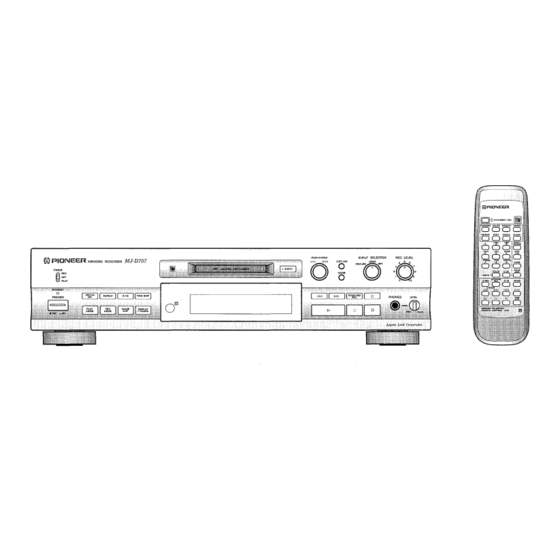
MJ-D707
MINIDISC RECORDER
$
) EJECT
TIMER
DISC LOADING MECHANISM
REC
OFF
PLAY
STANDBY
DIGITAL
REPEAT
A
B
TIME SKIP
POWER
NR
Î
PLAY
REC
NAME
DISPLAY
MODE
MODE
CLIP
/ CHARA
- OFF
_ ON
Power Requirement
Q Q
3
6 7
1 3
1 5
7. GENERAL INFORMATION .............................. 49
7.1 PARTS ....................................................... 49
7.1.1 IC ....................................................... 49
7.1.2 DISPLAY ........................................... 60
7.2 DIAGNOSIS ................................................ 61
7.2.1 DISASSEMBLY ................................. 61
7.2.2 DETAILS OF ERROR DISPLAY ....... 63
7.3 BLOCK DIAGRAM ...................................... 65
co
.
4-1, Meguro 1-Chome, Meguro-ku, Tokyo 153-8654, Japan
9 4
2 8
INPUT SELECTOR
REC LEVEL
$
EDIT
/
NO
COAX
5
ANALOG
OPT
4
6
3
7
2
8
NAME
1
9
0
10
!
!
SYNCHRO
REC
PHONES
LEVEL
#
*
&
MIN
MAX
Legato Link Conversion
Remarks
0 5
8
2 9
9 4
2 8
m
....................................................... 66
T-DZE JUNE 1998 Printed in Japan
9 9
ORDER NO.
RRV1963
9 9
Advertisement
Table of Contents


Need help?
Do you have a question about the MJ-D707 and is the answer not in the manual?
Questions and answers