Pioneer MJ-D508 Service Manual
Pioneer mj-d508 minidisc recorder service manual
Hide thumbs
Also See for MJ-D508:
- Service manual (6 pages) ,
- Operating instructions manual (49 pages) ,
- Operating instructions manual (48 pages)
Table of Contents
Advertisement
MINIDISC RECORDER
MJ-D508
THIS MANUAL IS APPLICABLE TO THE FOLLOWING MODEL(S) AND TYPE(S).
Model
Type
MJ-D508
‡
KUXJ
‡
MYXJ
‡
MYXJGR/FR
‡
NVXJ
CONTENTS
1. SAFETY INFORMATION .................................... 2
2. EXPLODED VIEWS AND PARTS LIST ............. 4
....................................................... 12
4. PCB CONNECTION DIAGRAM ....................... 28
5. PCB PARTS LIST ............................................. 37
6. ADJUSTMENT .................................................. 41
PIONEER ELECTRONIC CORPORATION
PIONEER ELECTRONICS SERVICE, INC. P.O. Box 1760, Long Beach, CA 90801-1760, U.S.A.
PIONEER ELECTRONIC (EUROPE) N.V . Haven 1087, Keetberglaan 1, 9120 Melsele, Belgium
PIONEER ELECTRONICS ASIACENTRE PTE. LTD. 253 Alexandra Road, #04-01, Singapore 159936
PIONEER ELECTRONIC CORPORATION 1999
POWER
- OFF - ON
Power Requirement
AC120V
AC220-230V
AC220-230V
AC230V
4-1, Meguro 1-Chome, Meguro-ku, Tokyo 153-8654, Japan
vC¿Û.?˘
MINIDISC RECORDER
REC/PLAY
MODE
EDIT/NO
NAME
DISC LOADING MECHANISM
0 EJECT
TIMER
REC OFF PLAY
INPUT
DAC
!
⁄
SYNCHRO
SELECTOR
MODE
REC
DIGITAL
NAME
DISPLAY
#
*
A-B
NR
CLIP
/CHARA
7. GENERAL INFORMATION .............................. 49
7.1 DIAGNOSIS ................................................ 49
7.1.1 TROUBLESHOOTING ...................... 49
7.1.2 DISASSEMBLY ................................. 52
7.2 PARTS ....................................................... 55
7.2.1 IC ....................................................... 45
7.2.2 DISPLAY ........................................... 66
....................................................... 68
DIGITAL
ANALOG
REC LEVEL
REC LEVEL
4
¢
5
4
6
3
7
2
8
1
9
0
10
ORDER NO.
PUSH ENTER
¶
PHONES
LEVEL
&
MIN
MAX
RRV2144
Remarks
T-ZZE MAY 1999 Printed in Japan
Advertisement
Table of Contents

Related Manuals for Pioneer MJ-D508


Summary of Contents for Pioneer MJ-D508
-
Page 1: Table Of Contents
PIONEER ELECTRONIC CORPORATION 4-1, Meguro 1-Chome, Meguro-ku, Tokyo 153-8654, Japan PIONEER ELECTRONICS SERVICE, INC. P.O. Box 1760, Long Beach, CA 90801-1760, U.S.A. PIONEER ELECTRONIC (EUROPE) N.V . Haven 1087, Keetberglaan 1, 9120 Melsele, Belgium PIONEER ELECTRONICS ASIACENTRE PTE. LTD. 253 Alexandra Road, #04-01, Singapore 159936 PIONEER ELECTRONIC CORPORATION 1999 T–ZZE MAY 1999 Printed in Japan... -
Page 2: Safety Information
, a l w a y s c o n s u l t t h e c u r r e n t P I O N E E R Service Manual. A subscription to, or additional copies Also test with plug reversed of, PIONEER Service Manual may be obtained at a (Using AC adapter Earth nominal charge from PIONEER. - Page 3 MJ-D508 IMPORTANT LASER DIODE CHARACTERISTICS THIS PIONEER APPARATUS CONTAINS MAXIMUM OUTPUT POWER: 27.4 mW LASER OF CLASS 1. WAVELENGTH: 785 nm SERVICING OPERATION OF THE APPARATUS S H O U L D B E D O N E B Y A S P E C I A L L Y INSTRUCTED PERSON.
-
Page 4: Exploded Views And Parts List
MJ-D508 2. EXPLODED VIEWS AND PARTS LIST NOTES : Parts marked by “ NSP ” are generally unavailable because they are not in our Master Spare Parts List. mark found on some component parts indicates the importance of the safety factor of the part. - Page 5 VEM–013 Polyethylene Bag Z21–038 (0.03 × 230 × 340) Warranty Card See Contrast table (2) (2) CONTRAST TABLE MJ-D508/KUXJ, MYXJ, MYXJGR/FR and NVXJ are constructed the same except for the following: Part No. Mark Remarks MJ-D508 Symbol and Description KUXJ...
- Page 6 MJ-D508 2.2 EXTERIOR KUXJ type only NVXJ type only MYXJ and MYXJGR/FR types only NVXJ type only Refer to “2.4 MD MECHANISM ASSY”. CN603 CN602 CN401 CN404 Except KUXJ type Refer to “2.3 FRONT PANEL SECTION”.
- Page 7 Bonnet PYY1271 Insulator PNW2766 POWER Button PAC1941 (POWER) Screw FBT40P080FZK (2) CONTRAST TABLE MJ-D508/KUXJ, MYXJ, MYXJGR/FR and NVXJ are constructed the same except for the following: Part No. Mark Remarks MJ-D508 Symbol and Description KUXJ MYXJ MYXJGR/FR NVXJ MAIN UNIT ASSY...
- Page 8 MJ-D508 2.3 FRONT PANEL SECTION 4 (1/3) 4 (2/3) 4 (3/3)
- Page 9 Screw ABA7009 Screw PPZ30P100FMC Lead Card 30P RDD1404 Acetate Cloth Tape ZTA-570F-21BK (2) CONTRAST TABLE MJ-D508/KUXJ, MYXJ, MYXJGR/FR and NVXJ are constructed the same except for the following: Part No. Mark Remarks MJ-D508 Symbol and Description KUXJ MYXJ MYXJGR/FR NVXJ...
- Page 10 MJ-D508 2.4 MD MECHANISM ASSY CN102 CN105 CN101 CN103...
- Page 11 MJ-D508 MD MECHANISM ASSY PARTS LIST Mark No. Description Part No. Mark No. Description Part No. CORE MAIN UNIT ASSY RWZ4334 Screw JGZ17P040FMC CORE SW UNIT ASSY RWZ4335 Screw PMB20P040FMC Lead Card 7P RDD1403 Servo Base Assy REA1283 Lead Wire...
-
Page 12: Block Diagram And Schematic Diagram
MJ-D508 3. BLOCK DIAGRAM AND SCHEMATIC DIAGRAM 3.1 BLOCK DIAGRAM POWER SUPPLY UNIT ASSY (RWZ4358 : KUXJ) (RWZ4363 : MYXJ, MYXJGR/FR, NVXJ) S201 SIGNAL ROUTE POWER CORD : PLAYBACK SIGNAL MY, NV : REC SIGNAL D201 IC202 : OUTPUT DIGITAL AUDIO SIGNAL... - Page 13 MJ-D508 Note : When ordering service parts, be sure to refer to "EXPLODED VIEWS and PARTS LIST" or "PCB PARTS LIST". MAIN UNIT ASSY 1/2, (RWZ4354 : KUXJ) AC1 AC2 (RWZ4359 : MYXJ, MYXJGR/FR, NVXJ) OPTICAL OUT INPUT OPTICAL IN 1...
- Page 14 MJ-D508 3.2 CORE MAIN UNIT and CORE SW UNIT ASSYS CORE MAIN UNIT ASSY (RWZ4334) CN101 PICKUP ASSY 10 11 (CARRIAGE)
- Page 15 MJ-D508 SIGNAL ROUTE : PLAYBACK SIGNAL ¶ 1 – - are waveform numbers on pages 26 and 27. : REC SIGNAL : OUTPUT DIGITAL AUDIO SIGNAL : INPUT DIGITAL AUDIO SIGNAL : RF SIGNAL CN104 CN401...
- Page 16 MJ-D508 Voltages of CORE MAIN UNIT ASSY IC101 IC102 IC103 IC104 VOLTAGE NO. VOLTAGE NO. VOLTAGE NO. VOLTAGE NO. VOLTAGE NO. VOLTAGE 0.78V 1.53V 1.59V 1.2V 3.2V 0.8V 0.73V 3.18V 1.2V 1.4V 0.77V 1.65V 3.0V 1.4V 0.75V 1.59V 2.0V 1.4V 1.61V...
- Page 17 MJ-D508 IC106 IC109 IC110 IC112 IC113 VOLTAGE NO. VOLTAGE NO. VOLTAGE NO. VOLTAGE NO. VOLTAGE 1.6V 2.77V 1.66V 4.95V 0.49V 2.77V 3.2V 1.62V 3.96V 1.61V 3.2V 1.62V 4.99V 1.58V 3.2V 4.99V 1.58V 1.67V 1.61V 1.56V 0.11V 1.67V 1.62V 1.67V 2.46V 3.19V...
- Page 18 MJ-D508 3.3 MAIN UNIT (1/2) C633, C634, C549, C550 : 220p (CH) and POWER SUPPLY UNIT ASSYS J704 : The power supply is shown with the marked box. CAUTION : FOR CONTINUED PROTECTION AGAINST RISK OF FIRE, REPLACE ONLY WITH SAME TYPE NO. 49102.5 MFD. BY LITTELFUSE INC.
- Page 19 MJ-D508 ¶ % is waveform number on page 27. MAIN UNIT ASSY (1/2) SIGNAL ROUTE (RWZ4354 : KUXJ) : PLAYBACK SIGNAL (RWZ4359 : MYXJ, MYXJGR/FR, NVXJ) : REC SIGNAL 400mA J901 400mA CAUTION : FOR CONTINUED PROTECTION AGAINST RISK OF FIRE, REPLACE ONLY WITH SAME TYPE NO.
- Page 20 MJ-D508 3.4 MAIN UNIT ASSY (2/2) CN701...
- Page 21 MJ-D508 ¶ = – $ are waveform numbers on page 27. SIGNAL ROUTE MAIN UNIT ASSY (2/2) : PLAYBACK SIGNAL (RWZ4354 : KUXJ) (RWZ4359 : MYXJ, MYXJGR/FR, NVXJ) : REC SIGNAL : OUTPUT DIGITAL AUDIO SIGNAL : INPUT DIGITAL AUDIO SIGNAL...
- Page 22 MJ-D508 3.5 DISPLAY UNIT, HEADPHONE UNIT and VOLUME UNIT ASSYS CN404 DISPLAY UNIT ASSY (RWZ4355 : KUXJ) (RWZ4360 : MYXJ MYXJGR/FR NVXJ)
- Page 23 MJ-D508 HEADPHONE UNIT ASSY (RWZ4357 : KUXJ) (RWZ4362 : MYXJ, MYXJGR/FR, NVXJ) VR901 : (HEADPHONE) LEVEL RCV1123 CN602 C904, C905, C907 : 0.1 (YF) VOLUME UNIT ASSY (RWZ4356 : KUXJ) (RWZ4361 : MYXJ, MYXJGR/FR, NVXJ) VR801 : ANALOG REC LEVEL...
- Page 24 MJ-D508 Voltages of MAIN UNIT ASSY (1kHz, 0dB, PLAY) IC401 IC402 IC403 IC404 IC602 NO. VOLTAGE NO. VOLTAGE NO. VOLTAGE NO. VOLTAGE NO. VOLTAGE NO. VOLTAGE 3.1V 2.5V 3.1V 2.5V 5.0V 5.0V 5.0V 2.5V 5.0V 2.5V 0.0V 1.5V 3.5V 5.0V 2.5V...
- Page 25 MJ-D508 Voltages of DISPLAY UNIT ASSY IC701 VOLTAGE VOLTAGE – 28.0V – 28.0V 5.0V 5.0V 0.6V 5.0V 4.9V 5.0V 0.0V 0.0V 5.0V 4.9V 4.9V 0.0V 5.0V Entire FL not lit – 30.7V 5.0V Entire FL lit 5.0V 0.1V 4.9V 2.5V 4.6V...
- Page 26 MJ-D508 Waveforms Note: The encircled numbers denote measuring point in the schematic diagram and the PCB connection diagram. IC101-pin35 (ADIPO) IC101-pin30 (WBO) IC102-pin1 (EFM MON) (CORE MAIN UNIT ASSY) (CORE MAIN UNIT ASSY) (CORE MAIN UNIT ASSY) MODE: PLAY MODE: PLAY MODE: PLAY DISC: GGF1328 (MMD–212)
- Page 27 MJ-D508 CN105-pin1 (LOAD –) IC602-pin28 (SYS CLK) IC602-pin19 (AD DATA) (CORE MAIN UNIT ASSY) (MAIN UNIT ASSY) (MAIN UNIT ASSY) MODE: EJECT MODE: STOP MODE: REC (ANALOG) DISC: GGF1328 (MMD-212) DC2V/div., 0.5 µSec/div. DC2V/div., 50nSec/div. DC1V/div., 1mSec/div. –– GND –– GND ––...
-
Page 28: Pcb Connection Diagram
MJ-D508 4. PCB CONNECTION DIAGRAM NOTE FOR PCB DIAGRAMS : 1. Part numbers in PCB diagrams match those in the schematic 3. The parts mounted on this PCB include all necessary parts for diagrams. several destinations. 2. A comparison between the main parts of PCB and schematic For further information for respective destinations, be sure to diagrams is shown below. - Page 29 MJ-D508 4.2 CORE MAIN UNIT ASSY ¶ 1 – - are waveform numbers on pages 26 and 27. CORE MAIN UNIT ASSY SIDE A 10 11 (RNP1733-B) IC101 IC106 IC102 IC103 IC104 IC114 Q101 Q102 SIDE B PICKUP ASSY (RNP1733-B)
- Page 30 MJ-D508 IC305 IC301 IC302 IC306 4.3 MAIN UNIT and POWER SUPPLY UNIT ASSYS MAIN UNIT ASSY CN104 SIDE A POWER SUPPLY UNIT ASSY POWER CORD...
- Page 31 MJ-D508 ¶ = – % are waveform numbers on page 27. IC604 IC603 IC307 IC601 SIDE A (RNP1732-C) CN701 J901 J801 (RNP1732-C)
- Page 32 MJ-D508 Q604 Q504 Q503 Q603 Q601 IC402 IC605 Q502 IC602 Q501 Q602 IC401 Q605 IC407 IC403 IC404 SIDE B (RNP1732-C) (RNP1732-C)
- Page 33 MJ-D508 Q304 MAIN UNIT ASSY SIDE B POWER SUPPLY UNIT ASSY...
- Page 34 MJ-D508 4.4 DISPLAY UNIT ASSY DISPLAY UNIT ASSY...
- Page 35 MJ-D508 CN404 SIDE A SIDE B (RNP1732-C)
- Page 36 MJ-D508 4.5 VOLUME UNIT and HEADPHONE UNIT ASSYS VOLUME UNIT ASSY (RNP1732-C) CN603 SIDE A SIDE B HEADPHONE UNIT ASSY (RNP1732-C) CN602...
-
Page 37: Pcb Parts List
MJ-D508 5. PCB PARTS LIST NOTES : Parts marked by “ NSP ” are generally unavailable because they are not in our Master Spare Parts List. mark found on some component parts indicates the importance of the safety factor of the part. - Page 38 Part No. Symbol and Description Remarks Mark RWZ4355 RWZ4360 R723 not used RS1/10S104J R724 RS1/10S104J not used PARTS LIST FOR MJ-D508/KUXJ Mark No. Description Part No. Mark No. Description Part No. C139 CEV101M4 CORE MAIN UNIT ASSY C166 CEV101M6R3 C147, C148, C201...
- Page 39 MJ-D508 Mark No. Description Part No. Mark No. Description Part No. C507, C508 CEAT220M50 CORE SW UNIT ASSY C614 CEAT221M6R3 C314 CEAT222M16 SWITCHES AND RELAYS C551, C552 CEAT2R2M50 C410 CEAT330M50 S701 RSF1009 S702 RSF1010 C313 CEAT332M16 C315, C444, C505, C506...
- Page 40 MJ-D508 Mark No. Description Part No. Mark No. Description Part No. COILS AND FILTERS HEADPHONE UNIT ASSY L206 LAU1R0J L204, L205 COIL RTF1167 COILS AND FILTERS L903 COIL RTF1167 CAPACITORS L901, L902 FERRITE BEADS VTH1020 C206 (10000pF/AC250V) ACG7020 C217 CEAT101M10...
-
Page 41: Adjustment
MJ-D508 6. ADJUSTMENT JIGS AND MEASURING INSTRUMENTS Thermometer Test Disc Oscilloscope For servo system adjustment ..........GGF1328 (MMD-212) Optical Power Meter For recording/playback inspection ....GGF1328 (MMD-212), GGF1277, Jitter Meter TGYS1 (or MMD-110), Commercial discs 6.1 NECESSARY ADJUSTMENT POINTS When... -
Page 42: Test Mode
MJ-D508 6.2 TEST MODE There are two test modes: test mode 1 for main unit operation check and test mode 2 for MD mechanism assy adjustment and check. 6.2.1 Test Mode 1 (main unit operation check) How to enter into test mode 1 1) Hold the “ENTER”... - Page 43 MJ-D508 6.2.2 Test Mode 2 (MD Mechanism Assy Adjustment, Check) Temperature Check (Please perform this check soon after the power has been switched on.) Note: When IC101 (RF-AMP), IC104 (mechanical controller) or IC110 (EEPROM) has been exchanged or when a correction changing VD+3 has been made, be sure to correctly perform all steps up to step 6.
- Page 44 MJ-D508 Grating Adjustment Step No. Operation Keys and Operation Method FL Display Status Remarks Power ON while holding the ENTER key and the PLAY EJECT Test mode key depressed. Insert the test disc GGF1328 (MMD-212). LOADING GRT AJST Grating adjustment status Press the PLAY key.
- Page 45 MJ-D508 4 Preliminary Adjustment Step No. Operation Keys and Operation Method FL Display Status Remarks Press the STOP key. AUT YOBI Return to menu display Press the EDIT/NO key. EEPROM W Writing to the EEPROM Toc Reading GGF1328 (MMD-212) Note: When this adjustment is performed after defocus adjustment has been performed, defocus is returned to the initial status, and defocus adjustment must be performed.
- Page 46 MJ-D508 6 Defocus adjustment Step No. Operation Keys and Operation Method FL Display Status Remarks Press the NAME CLIP key. of-04 c0020 The C1 error with application of a focus offset of about 0.4 µm on the – side is displayed.
- Page 47 MJ-D508 7 Jitter/C1 Error Check at the time of Playback Step No. Operation Keys and Operation Method FL Display Status Remarks Press the REC key. a006F c0017 The fixed display of the C1 error is ended. Press the STOP key.
- Page 48 MJ-D508 Jitter/C1 Error Check at the time of Recording/Playback Step No. Operation Keys and Operation Method FL Display Status Remarks Power ON while holding the ENTER key and the EJECT Test mode PLAY key depressed. Insert the test disc (GGF1277).
-
Page 49: General Information
MJ-D508 7. GENERAL INFORMATION 7.1 DIAGNOSIS 7.1.1 TROUBLESHOOTING 7 The power of the system does not turn to ON. Display does not light up. START POWER ON ¶ IC201(Protector) is open. ¶ Transformer temperrature fuse is open. ¶ IC201(SYSTEM CONTROL µCOM) is broken. - Page 50 MJ-D508 7 DETAILS OF ERROR DISPLAY Error Display Details of Error Measure ÷ DEFECT occurred 10 times continuously during REC-PLAY. ÷ Check if there are scratches, dusts, fingerprints, or black Can't REC ÷ Recordable cluster became 0 since DEFECT occurred during spots on disc.
- Page 51 MJ-D508 Details of Error Display Error Display Details of Error Measure ÷ Editing conditions were not satisfied for each editing function. ÷ Operating method is wrong. Try again using correct Can' t Edit method. ÷ Temperature inside unit (MD unit) was too high due to fault.
-
Page 52: Disassembly
MJ-D508 7.1.2 DISASSEMBLY Removal of the Servo Mechanism Assy 1 Remove the screw A and screw B. 2 Disconnect the connectors (CN102, CN103, CN105), open the hook of part A, and tilt the upper side of the CORE MAIN UNIT ASSY to the front. - Page 53 MJ-D508 Removal of the MD Pick-up Screw A 1 Remove the MD Head. (One screw A) (M1.7 × 4) 2 Remove the Screw Guide at the lower side of the MD Pick-up. (One screw B) MD Head Remove the hook after the 3 Remove the S.
- Page 54 MJ-D508 Removal of the Head Lifter Head Lifter Installation 1 Remove the Lifter SP. 1 Install part A in the Servo Base with the Head Lifter tilted to the 2 Tilt the Head Lifter to the rear and push part A to disengage it.
-
Page 55: Parts
MJ-D508 7.2 PARTS ¶ The information shown in the list is basic information and may not correspond exactly to that shown in the schematic diagrams. 7.2.1 IC M5M4V4400CTP-7 (IC103: CORE MAIN UNIT ASSY) DRAM Pin Assignment (Top view) Pin Function... - Page 56 MJ-D508 M56758FP (IC106: CORE MAIN UNIT ASSY) 5-channel Actuator Driver Block Diagram Pin Assignment (Top view) REG+ CH3IN VBS2 – IN3– VBS1 REGB OUT3 IN3+ IN1+ – OUT3 IN1+ IN3– IN1– OUT1 CH3IN VBS1 VBS2 VBS1 VBS2 VM1+ VM3+ –...
- Page 57 MJ-D508 PD5523A (IC104: CORE MAIN UNIT ASSY) Mechanism Control m-com. Pin Assignment (Top view) Block Diagram I/O PORT Port P0 Port P1 Port P2 Port P3 Port P4 Port P5 Port P6 Internal Peripheral A/D Converter Functions (10bits × 8 channels)
- Page 58 MJ-D508 Pin Function Name Description 1 to 7, 100 P96 to P90, P97 I/O These are 8 bit I/O ports with the same functions as P0. By software selection, it functions as the input terminals for the timers B0 to B2, the output terminals for the D/A converter, the expansion input terminals of the A/D converter, or the A/D trigger input terminals.
- Page 59 MJ-D508 Name Description 55 to 61, 63 P37 to P31, P30 I/O These are 8 bit I/O ports with the same functions as P0. A15 to A9, A8 The middle 8 bits (A8 to A15) of the address are put out.
- Page 60 MJ-D508 LR376487 (IC102: CORE MAIN UNIT ASSY) Encode/Decode/ATRAC Pin Assignment (Top view) 75 74 73 72 71 70 69 68 67 66 65 64 63 62 61 60 59 58 57 56 55 54 53 52 51 EFMO TOTMON PLCK...
- Page 61 MJ-D508 Name Description Name Description RAA4 Address output to external D-RAM; ADR4 Digital input signal DOUT Digital output signal RAA8 Address output to external D-RAM; ADR8 PLLBVC – Capacitor connection terminal for PLLB signal RAOEX Data output enable signal output to external D- DGND –...
- Page 62 MJ-D508 PDG240A (IC701: DISPLAY UNIT ASSY) System Control µ-com Pin Assignment (Top view) Block Diagram...
- Page 63 MJ-D508 Pin Function Name Description Name Description G1/A1 Output terminals used jointly for the FDP PD0/A55 timing signal (grid connection) and the G0/A0 segment signal (anode connection). PD7/A48 –– NC (connected to VDD) PF0/A47 PE0/INT0/EC0 PF7/A40 I/I/I Timer/counter external event input terminal...
- Page 64 MJ-D508 BD7910FV (IC116: CORE MAIN UNIT ASSY) Head Driver Block Diagram Name Description PDGND Predrive GND EFM signal input MUTE Mute control Pre Driver N.C. N.C. Not used N.C. VOD2 Sink output (lower side power MOS drain) H-bridge GND (lower side power MOS source)
- Page 65 MJ-D508 IR3R55M (IC101: CORE MAIN UNIT ASSY) RF Signal Processor Block Diagram Name Description ∗ XDISC Logic signal output terminal (outputs DISC signal inversion signal) ∗ XSGAIN Logic signal output terminal (outputs SGAIN signal inversion signal) AGND Analog part GND terminal...
-
Page 66: Display
MJ-D508 7.2.2 DISPLAY RAW1164 (V701: DISPLAY UNIT ASSY) Vacuum Fluorescent Display Pin Assignment Pin Connection Grid Assignment 9G 10G 11G 12G 13G DISC TRACK 9 10 TIME DATE 11 12 13 14 15 16 17 18 19 20 21 22 23 24 25 ADLC ALCA MONO A.MARK S.CUT SYNCHRO... - Page 67 MJ-D508...
-
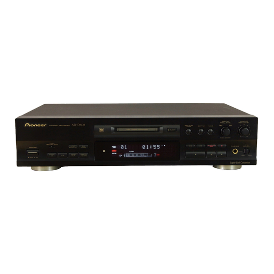
Page 68: Panel Facilities And Specifications
MJ-D508 8. PANEL FACILITIES AND SPECIFICATIONS 7 PANEL FACILITIES Front Panel 6 7 8 DIGITAL ANALOG REC LEVEL REC LEVEL vC¿Û.?˘ ¢ MINIDISC RECORDER REC/PLAY MODE EDIT/NO NAME DISC LOADING MECHANISM 0 EJECT PUSH ENTER TIMER REC OFF PLAY ⁄... - Page 69 MJ-D508 7 Front View...
- Page 70 MJ-D508 Display 2 3 4 5 6 7 DISC TRACK 9 10 TIME DATE 11 12 13 14 15 16 17 18 19 20 21 22 23 24 25 ADLC ALCA MONO A.MARK S.CUT SYNCHRO 1 REHEARSAL TOTAL REMAIN D.VOL...
-
Page 71: Remote Control
MJ-D508 Remote Control 8 A–B Use to set a start point and an end point to mark a section of the disc for editing or repeat play. 9 REPEAT Press to set the repeat mode (repeat disc, track, or segment). -
Page 72: Specifications
MJ-D508 7 SPECIFICATIONS Specifications Type ..............Minidisc digital audio system Recording system ........Field modulation overwrite system Reproduction system ..........Non-contact optical readout Sampling frequency ................44.1 kHz Frequency response ..............8 Hz to 20 kHz S/N ratio ..................... 100 dB Wow &...
Need help?
Do you have a question about the MJ-D508 and is the answer not in the manual?
Questions and answers