Chapters
Table of Contents
Troubleshooting

Related Manuals for Xerox Phaser 3110


Summary of Contents for Xerox Phaser 3110
-
Page 1: Table Of Contents
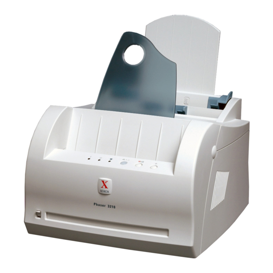
LASER PRINTER Phaser 3110 Phaser 3210 SERVICE Manual LASER PRINTER CONTENTS 1. Precautions 2. Specifications 3. Disassembly and Reassembly 4. Troubleshooting 5. Exploded Views and Parts List 6. Block Diagram 7. Connection Diagram 8. Electrical Parts List 9. Schematic Diagram - This Service Manual is a property of Samsung Electronics Co.,Ltd. -
Page 2: Precautions
Precautions 1. Precautions Please read the following carefully to prevent any accidents and not to damage the unit during service. 1-1 Safety Precautions 1. Safety Precautions LASER STATEMENT (LASERTURVALLISUUS) There are some electric or machinery parts with safety related property. If the parts replaced are dif- WARNING : NEVER OPERATE AND SERVICE THE PRINTER WITH THE PROTECTIVE COVER REMOVED ferent from the original, the safety may not function. -
Page 3: Tools For Troubleshooting
Precautions 1-3 Tools for Troubleshooting The following tools are recommended for safe and smooth troubleshooting described in this service manual. DCU(Diagnostic Control Unit) Driver Standard: Test equipment to diagnose the Laser Standard: "-" type, "+" type (M3 long, M3 short, printer supplied by Samsung Electronics. -
Page 4: Specifications
Specifications 2. Specifications Phaser 3110 Phaser 3210 Speed 10 ppm 12 ppm Engine Resolution 600 x 600 dpi 1200 dpi image quality true 600 x 600 dpi Fist Printing Time) Under 13 sec Warm-Up Time Under 30 sec Power Consumption... -
Page 5: Disassembly And Reassembly
Disassembly and Reassembly 3. Disassembly and Reassembly 3-1 Cover Assembly 3-1-1 Front Cover 1. Pull the both side of the cover to open. 4. Remove a screw of the front cover PCB and remove the connector, then remove the cover. 2. - Page 6 Disassembly and Reassembly 3-2 LED Panel PBA 1. Before you remove other covers, you should remove. 3. Remove two screws, and remove LED panel. • Front Cover (see [3-1 Main Cover]) 2. Remove two screws of PCB cover, and widen the hooks( a b c ) to remove.
-
Page 7: Transfer Roller
Disassembly and Reassembly 3-4 Transfer Roller 1. Open the front cover. 2. Use a proper tool("-" type screwdriver) to pull the one end of the roller slightly, then take it out. 3-5 Motor Assembly 1. Before you remove the motor assembly, you should remove: •... -
Page 8: Hvps Board
Disassembly and Reassembly 3-6 HVPS Board 1. Before you remove HVPS board, you should remove: •Main Cover (see [3-1 Main Cover]) 2. Remove four screws and a connector from HVPS board, then take the board out. When you reassemble the HVPS board, make sure that five terminals should be put in place. - Page 9 Disassembly and Reassembly 3-8 Thermostat and Halogen Lamp 1. Remove a screw from the fuser assembly and 3. Take the halogen lamp out from the Heat Roller. remove the thermostat cover, then remove two screws securing the thermostat. When you reassemble the halogen lamp, handle it with care as it is fragile.
-
Page 10: Smps Board
Disassembly and Reassembly 3-9 SMPS Board 1. Before you remove the SMPS board, you should 3. Unplug connectors from the main board and connec- remove: tors from SMPS, then remove the SMPS. Remove four screws from SMPS and remove the SMPS •... - Page 11 Disassembly and Reassembly 3-10 Main Board and Sensor Board 1. Before you remove the main board, you should 3. Release four snap-fits securing the insulator engine remove: board and then remove the insulator. • Main Cover (see [3-1 Main Cover]) •...
-
Page 12: Troubleshooting
Troubleshooting 4. Troubleshooting 4-1 How to use DCU 4-4 The cause and solution of the malfunction 4-1-1 DCU Setup ........Page(4-2) 4-4-1 All LEDs blinking (Fuser Error)..Page(4-16) 4-1-2 Code ..........Page(4-2) 4-4-2 All LEDs blinking (SCAN ERROR) .Page(4-16) 4-1-3 Self Diagnostic Mode......Page(4-3) 4-4-3 Not function of the gear of the fuser due to melting away........Page(4-17) 4-1-4 Self Test Button ........Page(4-4) -
Page 13: How To Use Dcu
Troubleshooting 4-1 How to use DCU 4-1-1 DCU Setup You can examine the malfunction of the printer. To perform DCU, open the front discharge cover and leave the connect the harness wire(10 pin/4 pin) to the CN10(4 pin) of the Main control board. 4-1-2 Code Connect DCU to the printer and turn the power on. -
Page 14: Self Diagnostic Mode
Troubleshooting 4-1-3 Self Diagnostic Mode If Error code occurs due to malfunction of the printer, perform Self Diagnostic Mode to solve the problem. The printer works only in the self-test mode to solve the malfunction problem. To enter the self-test mode, turn the power on pressing the buttons of [Down], [Shift] and [Stop] at the same time. Release the button within 2 or 3 seconds if 78 shows in the DCU. -
Page 15: Self Test Button
Troubleshooting THV(+) TRIGGER. ALL HV All high voltage output by each HV terminal and LSU and the fan is in operation. In this mode, electronic resistance of transfer roller and high voltage is detected. If no toner cartridge in the printer, output of THV is +199V ~ + 2100V. -
Page 16: The Cause And Solution Of Bad Image
Troubleshooting 4-2 The cause and solution of Bad image 4-2-1 Vertical Black Line and Band 1. Straight thin black vertical line occurs in the printing. • Description 2. Dark black vertical band occur in the printing. Check and Cause Solution Digital Printer 1. -
Page 17: Horizontal Black Band
Troubleshooting 4-2-3 Horizontal Black Band 1. Dark or blurry horizontal stripes occur in the printing periodically. • Description (They may not occur periodically.) Check and Cause Solution Digital Printer 1. Bad contacts of the voltage terminals to 1. Clean each voltage terminal of the Charge, Digital Printer developer. -
Page 18: Light Image
Troubleshooting 4-2-5 Light Image • Description The printed image is light, with no ghost. Check and Cause Solution Digital Printer 1. Develop roller is stained when the toner 1. Check if the Toner Save mode is off. Digital Printer of developer cartridge is almost con- Digital Printer sumed. -
Page 19: Uneven Density
Troubleshooting 4-2-7 Uneven Density • Description Print density is uneven between left and right. Check and Cause Solution 1. The pressure force on the left and right 1. Replace both the left and right Spring springs of the transfer roller is not even, Holder. -
Page 20: Ghost (1)
Troubleshooting 4-2-9 Ghost (1) • Description Ghost occurs at 75 mm intervals of the OPC drum in the whole printing. Check and Cause Solution Digital Printer Digital Printer 1. Bad contacts caused by contamination 1. Clean the terminals when contaminated by Digital Printer from toner particles between high voltage toner particles. -
Page 21: Ghost (3)
Troubleshooting 4-2-11 Ghost (3) 4-2-11 Ghost (3) • Description • Description White ghost occurs in the black image printing at 32mm intervals. White ghost occurs in the black image printing at 32mm intervals. Check and Cause Check and Cause Solution Solution Digital Printer Digital Printer... -
Page 22: Satins On Back Of Page
Troubleshooting 4-2-14 Satins on Back of Page • Description The back of the page is stained at 47mm intervals. Check and Cause Solution Digital 1. Transfer roller is contaminated. 1. Perform the OPC Cleaning Mode Print 2 or Digital Pri 3 times. -
Page 23: The Cause And Solution Of The Bad Discharge
Troubleshooting 4-3 The cause and solution of the bad discharge 4-3-1 Wrong Print Position • Description Printing begins at wrong position on the paper. Check and Cause Solution Wrong sense time caused by defective feed sensor Replace the defective actuator actuator. -
Page 24: Jam 1
Troubleshooting 4-3-3 JAM 1 1. Recording paper is jammed in front of or inside the fuser. • Description 2. Recording paper is stuck in the discharge roller and in the fuser just after passing through the Actuator-Feed. Check and Cause Solution 1. -
Page 25: Multi-Feeding
Troubleshooting 4-3-5 Multi-Feeding • Description Multiple sheets of paper are fed at once. Check and Cause Solution 1. Solenoid malfunction(the solenoid does not work 1. Replace the solenoid if necessary. properly): Perform DCU mode : solenoid check 06. (Service Parts : Figure 13, chapter 5) 2. -
Page 26: Opc
Troubleshooting 4-3-7 OPC • Description Paper is rolled up in the OPC. Check and Cause Solution 1. Paper is too much thin. 1. Recommend to use normal paper. 2. The face of paper is curled. 2. How to remove the rolled paper in the OPC. •... -
Page 27: The Cause And Solution Of The Malfunction
Troubleshooting 4-4 The cause and solution of the malfunction 4-4-1 All LEDs blinking (Fuser Error) 1. All the lamps on the operator panel blink. • Description 2. Gear of the fuser does not work and breaks away melt away. When printing, motor breaks away from its place due to defective fuser gear. Check and Cause Solution 1. -
Page 28: Not Function Of The Gear Of The Fuser Due To Melting Away
Troubleshooting 4-4-3 Not function of the gear of the fuser due to melting away • Description The motor breaks away from its place due to gear melting away. Check and Cause Solution DCU Mode : Check if the Error States '60' '62' '68' occur. 1. -
Page 29: Cover Open
Troubleshooting 4-4-6 Cover Open • Description The ERROR lamp is on even when the print cover is closed. Check and Cause Solution 1. The hook lever in the top cover may be defective. 1. Replace the hook lever, if defective. (Service Parts : Figure 1, chapter 5) 2. -
Page 30: Defective Motor Operation
Troubleshooting 4-4-9 Defective motor operation • Description Main motor is not driving when printing, and paper does not feed into the printer, resulting 'Jam 0'. Check and Cause Solution 1. Motor harness or sub PCB may be defective. 1. Check the motor harness, replace it, if defective. (Service Parts : Figure 12, chapter 5) 2. -
Page 31: Vertical Line Getting Curved
Troubleshooting 4-4-11 Vertical Line Getting Curved • Description When printing, vertical line gets curved. Check and Cause Solution 1. If the supply of +24v is unstable in the Main Control board 1. Replace LSU. linking with LSU, check drive by DCU Mode: LSU Check (Service Parts : Figure 13, chapter 5) -05- LSU Motor on. -
Page 32: Toner Cartridge Service
Troubleshooting 4-5 Toner Cartridge Service It is not guaranteed for the default caused by using other toner cartridge other than the cartridge supplied by the Samsung Electronic or caused by non-licensed refill production. 4-5-1 Precautions on Safe-keeping of Toner Cartridge Excessive exposure to direct light more than a few minutes may cause damage to the cartridge. -
Page 33: Signs And Measures At Poor Toner Cartridge
Troubleshooting 4-5-3 Signs and Measures at Poor toner cartridge Fault Signs Cause & Check Solution Light image and • The printed image 1. If the image is light or unclean 1. All of 1, 2, 3 above- partially blank is light or unclean and untidy printed image - (1)The weight of the developer image... - Page 34 Troubleshooting Fault Signs Cause & Check Solution 1. If light or dark periodical black White Black spot • Light or dark black 1. In case of 1 above - dots occur, this is because the dots on the image Run OPC Cleaning Mode Print developer rollers are contami- occur periodically.
- Page 35 Troubleshooting Fault Signs Cause & Check Solution Ghost & Image • The printed image 1. The printed image is too light 1. All of 1, 2, 3 above Contamination is too light or dark, or dark, or partially contami- (1)Remove toner and foreign sub- or partially contami- nated black.
-
Page 36: The Cause And Solutions Of Bad Environment Of The Software
Troubleshooting 4-6 The cause and solutions of bad environment of the software 4-6-1 The printer is not working (1) • Description While Power turned on, the printer is not working in the printing mode. Check and Cause Solution 1. Run Self-Test Mode: Turn the power on while pressing 1.Check the power of the printer and perform the Self- the test printing button for 2 or 3 seconds before printing Test. -
Page 37: The Printer Is Not Working (2)
Troubleshooting 4-6-2 The printer is not working (2) After receiving the printing order, no response at all or the low speed of printing • Description occurs due to wrong setup of the environment rather than malfunction of the printer itself. Check and Cause Solution 1. -
Page 38: Abnormal Printing
Troubleshooting 4-6-3 Abnormal Printing The printing is not working properly even when the cable has no problem. (even after the cable is replaced) • Description If the printer won't work at all or the strange fonts are repeated, the printer driver may be defec- tive or wrong setup in the CMOS Setup. -
Page 39: Spool Error
Troubleshooting 4-6-4 SPOOL Error To spool which stands for "simultaneous peripheral operations online" a computer document or task list (or "job") is to read it in and store it, usually on a hard disk or larger storage medium so • Description that it can be printed or otherwise processed at a more convenient time (for example, when a printer is finished printing its current document). -
Page 40: Exploded Views And Parts List
Exploded Views and Parts List 5. Exploded Views and Parts List • Deal drawings and service parts are declared for the items with higher rate of inferiority and replaceable in the level of service description only. • If inferiority occurs, you can replace the parts by the unit declared in deal drawings and service items. -
Page 41: Tatal Assembly
Exploded Views and Parts List 5-1 Tatal Assembly... -
Page 42: Service Parts List
PMO-BUSHING SHAFT JC72-40849A 8-28 MEC-ROLLER FEED JC75-00054A 8-29 EMC-HOLDER FEED JC75-00055A 8-30 PMO-HOLDER TR JC72-00100D PBA MAIN-CONTROLLER GDI JC92-01316A Phaser 3110 PBA MAIN-CONTROLLER PCL JC92-01333A Phaser 3210 SMPS-ML-1210 V2 JC96-02234B 220V SMPS-ML-1210 V1 JC96-02233C 110V SMPS-HVPS GDI JC44-00024A Phaser 3110... -
Page 43: Front Assembly
Exploded Views and Parts List 5-2 Front Assembly DESCRIPTION ELA HOU-COVER FRONT CBF-HARNESS-PANEL MAIN PMO-COVER FRONT PMO-GUIDE STACKER PMO-DOOR FACE UP PPR-SHEET PAPER GUIDE PMO-KEY A PMO-KEY B PMO-LENS SED PMO-COVER PCB PMO-STOPPER PMO-BRKT PUSH DEVE PBA SUB DISP-PANEL PMO-COVER FRONT, SUB IMAC... -
Page 44: Engine/Frame Lower Assembly
Exploded Views and Parts List 5-3 Engine/Frame Lower Assembly 2-17 2-14 2-13 2-3-2 2-12 3-2-2 3-2-3 3-2-1 2-11 2-3-1 3-2-4 3-15 3-43 2-15 3-44 3-12 3-3-1 3-2-3 2-7-3 2-7-1 3-2-1 2-10 2-7-2 2-16 2-16-2 3-17 2-16-1 2-9-1 3-10-2 3-10-1 3-10 2-9-2 3-41 2-9-3... -
Page 45: Fuser Assembly
Exploded Views and Parts List 5-4 Fuser Assembly DESCRIPTION ELA HOU-FUSER ASS’Y THERMISTOR-NTC THERMOSTAT-150C LAMP-HALOGEN PMO-COVER FUSER PMO-BUSHING H/R, L PMO-BUSHING H/R, R PMO-COVER_THERMOSTAT NPR-ROLLER HEAT IPR-ELECTRODE_PLATE IPR-GROUND_FU PMO-GUIDE CLAW 15-2 ELECTRODE-WIRE,1 15-1 ELECTRODE-WIRE,S MEA ETC-SHAFT EXIT 14-1 PMO-SHAFT_EXIT(Z15) 14-1 14-2 14-2 RMO-RUBBER_EXIT... -
Page 46: Shield Engine Unit Assembly
Exploded Views and Parts List 5-5 Shield Engine Unit Assembly DESCRIPTION ELA HOU-SHIELD ENGINE MEC-SHIELD BRKT CONTROLLER IPR-SHIELD ENGINE IPR-BRKT CONTROLLER PCT-INSULATOR SMPS CBF HARNESS-INLET ASS’Y SCREW-MACHINE SCREW-TAPTITE SCREW-TAPTITE... -
Page 47: Rx Drive Assembly
Exploded Views and Parts List 5-6 RX Drive Assembly DESCRIPTION ELA HOU-RX DRIVE MOTOR-STEP PMO-GEAR_71/28 PMO-GEAR_73/22 PMO-GEAR_132/19 IPR-BRKT_MOTOR IPR-BRKT_GEAR CBF-HARNESS_MOTOR SCREW-MACHINE 5-7 Plate-Upper Unit Assembly DESCRIPTION MEC-PLATE UPPER IPR-UPPER-PLATE IPR-PLATE SPRING DEV MEA ETC-ROLLER PICKUP PMO-HOUSING_PICKUP RMO-ROLLER_PICKUP PMO-IDLE_PICKUP MEA ETC-IDLE FEED PMO-HOLDER_PICKUP SPRING-FEED PMO-HOLDER_IDLE,FEED... -
Page 48: Block Diagram
Block Diagram 6. Block Diagram 6-1. Block Diagram(GDI) MAIN POWER SWI TCH POWER SMPS 74LVX161284 +24V FLASH CORD Line I N-LET IEEE 1284 CABLE MEMORY EXI T Transcei ver (0 .5MB) SE N SOR MOTOR SDRAM Power (8MB) Engine SOLENOIDE Res et VOLTAGE DETECT OR... - Page 49 Block Diagram 6-2. Block Diagram(PCL) MAIN Oscillator POWER 48 MHz SWITCH SMPS POWER +24V USB Driver FLASH CORD IN-LET IEEE 1284 CABLE USBN9602-28M MEMORY EXIT (2MB) SE N SOR MOTOR DRAM Power Engine SOLENOID Reset VOLTAGE Option DETECTOR Up to C P U 68MB DEV_FUSE...
-
Page 50: Connection Diagram
Connection Diagram 7. Connection Diagram 7-1. Connection Diagram(GDI) +24V_T +24V GND IEEE1284 POLYGON *PMOTOR COMPA TI ABLE MOTOR +3. 3V CABLE EXT_C LK * HSYNC PI N +5V GND LD DIODE * LD_ON +5V GND 4PI N HOST USB CABLE CONN- +5V GND COMPUTER... - Page 51 Connection Diagram 7-2. Connection Diagram(PCL) +24V_SLEEP +24V GND IEEE1284 POLYGON MOTOR COMPATI ABLE MOTOR LREADY* CABLE EXT_C LK HSYNC CN12 PI N +5V GND LD DIODE LD_ON +5V GND 4PI N HOST USB CABLE CONN- +5V GND COMPUTER ECTOR LED_ERROR f or LED_PAPER U SB...
-
Page 52: Electrical Parts List
Electrical parts list 8. Electrical parts list 8-1 Main PBA (Phaser 3110) SEC CODE LOCATION NO. Q’ty DESCRIPTION 0105-001032 PAPER-ART “75g,W210,-,WHITE,HANSOI,L297” 0401-000116 DIODE-SWITCHING “MMSD914T1,100V,200mA,SOD-123,TP” 0401-000116 DIODE-SWITCHING “MMSD914T1,100V,200mA,SOD-123,TP” 0404-000112 DIODE-SCHOTTKY “RB420D,25V,100mA,SOT-23,TP” 0407-000101 “D14,D15,D16,D17,D18” DIODE-ARRAY “DA204K,20V,100mA,C2-3,SOT-23,T” 0501-000338 TR-SMALL SIGNAL “2SC2812,NPN,200mW,SOT-23,TP,20” 0501-000338 TR-SMALL SIGNAL “2SC2812,NPN,200mW,SOT-23,TP,20”... - Page 53 Electrical parts list SEC CODE LOCATION NO. Q’ty DESCRIPTION 2007-000090 R-CHIP “10KOHM,5%,1/16W,DA,TP,1608” 2007-000090 R-CHIP “10KOHM,5%,1/16W,DA,TP,1608” 2007-000090 R-CHIP “10KOHM,5%,1/16W,DA,TP,1608” 2007-000090 R-CHIP “10KOHM,5%,1/16W,DA,TP,1608” 2007-000090 R-CHIP “10KOHM,5%,1/16W,DA,TP,1608” 2007-000090 R-CHIP “10KOHM,5%,1/16W,DA,TP,1608” 2007-000090 R-CHIP “10KOHM,5%,1/16W,DA,TP,1608” 2007-000090 “R80,R92,R93” R-CHIP “10KOHM,5%,1/16W,DA,TP,1608” 2007-000090 R-CHIP “10KOHM,5%,1/16W,DA,TP,1608” 2007-000113 “R27,R4,R5” R-CHIP “33ohm,5%,1/16W,DA,TP,1608”...
- Page 54 Electrical parts list SEC CODE LOCATION NO. Q’ty DESCRIPTION 2203-000192 “C96,C89” “C-CERAMIC,CHIP” “100nF,+80-20%,50V,Y5V,TP,2012,” 2203-000236 “C134,C188,C192,C194” “C-CERAMIC,CHIP” “0.1nF,5%,50V,NP0,TP,1608” 2203-000236 “C154,C156,C157,C158” “C-CERAMIC,CHIP” “0.1nF,5%,50V,NP0,TP,1608” 2203-000257 “C102,C146” “C-CERAMIC,CHIP” “10nF,10%,50V,X7R,TP,1608” 2203-000257 “C126,C127,C128,C130,C136,C137” “C-CERAMIC,CHIP” “10nF,10%,50V,X7R,TP,1608” 2203-000257 “C18,C85,C15,C21,C26,C123,C125” “C-CERAMIC,CHIP” “10nF,10%,50V,X7R,TP,1608” 2203-000257 “C-CERAMIC,CHIP” “10nF,10%,50V,X7R,TP,1608” 2203-000257 “C-CERAMIC,CHIP” “10nF,10%,50V,X7R,TP,1608” 2203-000257 “C-CERAMIC,CHIP”...
- Page 55 Electrical parts list 8-2 Main PBA (Phaser 3210) SEC CODE LOCATION NO. Q’ty DESCRIPTION JC92-01333A PBA MAIN-PCL “ML-1250,SEC,WORLD WIDE,PCL,12PPM,” 0105-001032 PAPER-ART “75g,W210,-,WHITE,HANSOI,L297” 0401-000116 DIODE-SWITCHING “MMSD914T1,100V,200mA,SOD-123,TP” 0401-000116 DIODE-SWITCHING “MMSD914T1,100V,200mA,SOD-123,TP” 0404-000112 DIODE-SCHOTTKY “RB420D,25V,100mA,SOT-23,TP” 0407-000101 DIODE-ARRAY “DA204K,20V,100mA,C2-3,SOT-23,T” 0407-000101 DIODE-ARRAY “DA204K,20V,100mA,C2-3,SOT-23,T” 0501-000338 TR-SMALL SIGNAL “2SC2812,NPN,200mW,SOT-23,TP,20”...
- Page 56 Electrical parts list SEC CODE LOCATION NO. Q’ty DESCRIPTION 2007-000078 R-CHIP “1Kohm,5%,1/16W,DA,TP,1608” 2007-000078 R-CHIP “1Kohm,5%,1/16W,DA,TP,1608” 2007-000084 R-CHIP “4.7Kohm,5%,1/16W,DA,TP,1608” 2007-000086 R-CHIP “5.6Kohm,5%,1/16W,DA,TP,1608” 2007-000086 R-CHIP “5.6Kohm,5%,1/16W,DA,TP,1608” 2007-000090 R100 R-CHIP “10KOHM,5%,1/16W,DA,TP,1608” 2007-000090 R126 R-CHIP “10KOHM,5%,1/16W,DA,TP,1608” 2007-000090 R134 R-CHIP “10KOHM,5%,1/16W,DA,TP,1608” 2007-000090 R135 R-CHIP “10KOHM,5%,1/16W,DA,TP,1608” 2007-000090 R136 R-CHIP...
- Page 57 Electrical parts list SEC CODE LOCATION NO. Q’ty DESCRIPTION 2011-001334 RC-NETWORK “1K/5.1K/39ohm,10%,150pF,-,6V,28P” 2203-000189 C100 “C-CERAMIC,CHIP” “100nF,+80-20%,25V,Y5V,TP,1608,” 2203-000189 C101 “C-CERAMIC,CHIP” “100nF,+80-20%,25V,Y5V,TP,1608,” 2203-000189 C105 “C-CERAMIC,CHIP” “100nF,+80-20%,25V,Y5V,TP,1608,” 2203-000189 C107 “C-CERAMIC,CHIP” “100nF,+80-20%,25V,Y5V,TP,1608,” 2203-000189 C108 “C-CERAMIC,CHIP” “100nF,+80-20%,25V,Y5V,TP,1608,” 2203-000189 C109 “C-CERAMIC,CHIP” “100nF,+80-20%,25V,Y5V,TP,1608,” 2203-000189 C110 “C-CERAMIC,CHIP” “100nF,+80-20%,25V,Y5V,TP,1608,” 2203-000189 C113 “C-CERAMIC,CHIP”...
- Page 58 Electrical parts list SEC CODE LOCATION NO. Q’ty DESCRIPTION 2203-000189 “C-CERAMIC,CHIP” “100nF,+80-20%,25V,Y5V,TP,1608,” 2203-000189 “C-CERAMIC,CHIP” “100nF,+80-20%,25V,Y5V,TP,1608,” 2203-000189 “C-CERAMIC,CHIP” “100nF,+80-20%,25V,Y5V,TP,1608,” 2203-000189 “C-CERAMIC,CHIP” “100nF,+80-20%,25V,Y5V,TP,1608,” 2203-000189 “C-CERAMIC,CHIP” “100nF,+80-20%,25V,Y5V,TP,1608,” 2203-000189 “C-CERAMIC,CHIP” “100nF,+80-20%,25V,Y5V,TP,1608,” 2203-000189 “C-CERAMIC,CHIP” “100nF,+80-20%,25V,Y5V,TP,1608,” 2203-000189 “C-CERAMIC,CHIP” “100nF,+80-20%,25V,Y5V,TP,1608,” 2203-000189 “C-CERAMIC,CHIP” “100nF,+80-20%,25V,Y5V,TP,1608,” 2203-000189 “C-CERAMIC,CHIP” “100nF,+80-20%,25V,Y5V,TP,1608,” 2203-000189 “C-CERAMIC,CHIP”...
- Page 59 Electrical parts list SEC CODE LOCATION NO. Q’ty DESCRIPTION 2203-000440 “C-CERAMIC,CHIP” “1nF,10%,50V,X7R,TP,1608,-” 2203-000440 “C-CERAMIC,CHIP” “1nF,10%,50V,X7R,TP,1608,-” 2203-000440 “C-CERAMIC,CHIP” “1nF,10%,50V,X7R,TP,1608,-” 2203-000440 “C-CERAMIC,CHIP” “1nF,10%,50V,X7R,TP,1608,-” 2203-000440 “C-CERAMIC,CHIP” “1nF,10%,50V,X7R,TP,1608,-” 2203-000440 “C-CERAMIC,CHIP” “1nF,10%,50V,X7R,TP,1608,-” 2203-000440 “C-CERAMIC,CHIP” “1nF,10%,50V,X7R,TP,1608,-” 2203-000440 “C-CERAMIC,CHIP” “1nF,10%,50V,X7R,TP,1608,-” 2203-000440 “C-CERAMIC,CHIP” “1nF,10%,50V,X7R,TP,1608,-” 2203-000626 C104 “C-CERAMIC,CHIP” “0.022nF,5%,50V,NP0,TP,1608” 2203-000626 “C-CERAMIC,CHIP”...
- Page 60 Electrical parts list SEC CODE LOCATION NO. Q’ty DESCRIPTION 3301-000317 CORE-FERRITE BEAD “AB,2x1.25x0.9mm,-,-” 3301-000344 CORE-FERRITE BEAD “AA,-,3.5x0.6x6.5mm,-,-,Mn-Zn,-” 3301-001069 CORE-FERRITE BEAD “AB,1.6x0.8x0.8mm,-,-” 3301-001069 CORE-FERRITE BEAD “AB,1.6x0.8x0.8mm,-,-” 3301-001069 CORE-FERRITE BEAD “AB,1.6x0.8x0.8mm,-,-” 3301-001069 CORE-FERRITE BEAD “AB,1.6x0.8x0.8mm,-,-” 3301-001069 CORE-FERRITE BEAD “AB,1.6x0.8x0.8mm,-,-” 3702-000118 CONNECTOR-RIBBON “36P,FEMALE,ANGLE,AU” 3709-000177 CONNECTOR-CARD EDGE “72P,1.27mm,ANGLE,SN”...
-
Page 61: Schematic Diagram
Schematic Diagrams 9. Schematic Diagrams 9-1 GDI Main Circuit Diagram(1/5) - This Document can not be used without Samsung's authorization -... - Page 62 Schematic Diagrams GDI Main Circuit Diagram(2/5) - This Document can not be used without Samsung's authorization -...
- Page 63 Schematic Diagrams GDI Main Circuit Diagram(3/5) - This Document can not be used without Samsung's authorization -...
- Page 64 Schematic Diagrams GDI Main Circuit Diagram(4/5) - This Document can not be used without Samsung's authorization -...
- Page 65 Schematic Diagrams GDI Main Circuit Diagram(5/5) - This Document can not be used without Samsung's authorization -...
- Page 66 Schematic Diagrams 9-2 PCL Main Circuit Diagram(1/9) - This Document can not be used without Samsung's authorization -...
- Page 67 Schematic Diagrams PCL Main Circuit Diagram(2/9) - This Document can not be used without Samsung's authorization -...
- Page 68 Schematic Diagrams PCL Main Circuit Diagram(3/9) - This Document can not be used without Samsung's authorization -...
- Page 69 Schematic Diagrams PCL Main Circuit Diagram(4/9) - This Document can not be used without Samsung's authorization -...
- Page 70 Schematic Diagrams PCL Main Circuit Diagram(5/9) 9-10 - This Document can not be used without Samsung's authorization -...
- Page 71 Schematic Diagrams PCL Main Circuit Diagram(6/9) 9-11 - This Document can not be used without Samsung's authorization -...
- Page 72 Schematic Diagrams PCL Main Circuit Diagram(7/9) 9-12 - This Document can not be used without Samsung's authorization -...
- Page 73 Schematic Diagrams PCL Main Circuit Diagram(8/9) 9-13 - This Document can not be used without Samsung's authorization -...
- Page 74 Schematic Diagrams PCL Main Circuit Diagram(9/9) 9-14 - This Document can not be used without Samsung's authorization -...
- Page 75 Schematic Diagrams 9-3 Panel Circuit Diagram 9-15 - This Document can not be used without Samsung's authorization -...
- Page 76 Schematic Diagrams 9-4 HVPS Circuit Diagram(1/2) 24VS C402 R407 R401 240K T401 D401 C404 R426 KAB-006 R405 3KV 471 R411 MGR1/2W 100KF R422 220KF 2.2K 5.6K R403 R404 R413 110KF Q401 Q402 MGR1/2W 6MF A708-Y D526-Y C406 MHV-PWM 3KV 471 R416 C405 D402...
- Page 77 Schematic Diagrams HVPS Circuit Diagram(2/2) T201 C208 C206 24VS HVT-2A 6KV 471 6KV 471 D204 D206 R201 D207 D205 R206 Q204 D526-Y THV-PWM C205 D201 U1-B C209 C207 R208 6KV 101 1N4148 KA324 6KV 471 30KF 6KV 471 R205 CN1-#3 R213 U2-F U2-E...
- Page 78 Schematic Diagrams 9-5 SMPS Circuit Diagram(100V) R502 V501 F501 F502 1/2W T501 R518 C522 LF501 LF502 SCK-054 125V 8A 560K 125V 3A EER2828 1KV 102 APOLLO12 APOLLO12 CN501 C501 D504 R517 C508 R509 222MAD R505 ER1002FCT CN5-7,9,11 +24V 1.8A C511 BD501 FL406 C520...
- Page 79 Schematic Diagrams SMPS Circuit Diagram(200V) R502 V501 F501 F502 R518 C522 1/2W T501 LF501 LF502 250V 5A SCK-054 250V 2A 1KV 102 560K EER2828 APOLLO12 APOLLO12 CN501 D504 C501 R517 R509 C508 R505 222MAD ER1002FCT CN5-7,9,11 100K C511 +24V 1.8A BD501 FL406 C520...
Need help?
Do you have a question about the Phaser 3110 and is the answer not in the manual?
Questions and answers