Table of Contents
Advertisement
Quick Links
Advertisement
Table of Contents

Subscribe to Our Youtube Channel
Related Manuals for Oki TF-300P


Summary of Contents for Oki TF-300P
- Page 1 TF-300P Field Service Manual Ver. 02 July 8, 1999 TTIC...
- Page 2 Index 1. INTRODUCTION TANDARD PECIFICATIONS ENERAL UNCTION ENERAL PPEARANCE 1.3.1 PPEARANCE 1.3.2 HOW THE OPERATION PANEL ENERAL AINTENANCE UNCTION 2. INSTALLATIONS ENERAL ELECTION NPACKING HECK OF ONTENTS NSTALLATION OF TTACHMENTS 2.5.1 SIM C ARTRIDGE AND 2.5.2 ANDSET AND 2.5.3 AC C ONNECTION 2.5.4 OADING...
- Page 3 5.3.6 CANNER 5.3.7 CANNER 5.3.8 OWER RAME 5.3.9 PPER RAME 5.3.10 OCUMENT UIDE SSEMBLY 5.3.11 PERATION ANEL 5.3.12 PPER OVER 5.3.13 RINTER 5.3.14 RINTER 5.3.15 APER EEDER 5.3.16 5-10 RAME 5.3.17 5-11 OTTOM OVER 6. CIRCUIT DESCRIPTION OARD IRCUIT 6.1.1 LOCK IAGRAM 6.1.2...
- Page 4 6.5.5 6-18 ESSAGE RANSMITTING 6.5.6 6-18 UILT ANDSET AND ERIAL QUIPMENT ETECTION 6-18 ELEPHONE IRCUIT IAGRAM ESCRIPTION 6.6.1 6-18 ENERAL FUNCTIONS OF TELEPHONE CIRCUIT 6.6.2 IC AS2534 6-18 ELEPHONE GENERAL DESCRIPTION 6.6.3 6-19 INGING 6.6.4 DTMF D 6-19 IALLING 6.6.5 6-19 ULSE IALLING...
- Page 5 7.22 7-17 OTOR EMAINS OTIONLESS 7.23 7-17 RINTING WITH 7.24 SIMCARD I 7-18 NVALID 7.25 7-19 ROUBLE HOOTING ECHANICAL ROBLEM 7.26 NCU/TEL B 7-22 OARD ROUBLE HOOTING 7.26.1 7-22 INGING 7.26.2 7-22 IALLING 7.26.3 7-22 ANDSET FUNCTION 8. PART LIST OARD OARD RINT...
-
Page 6: Introduction
1. INTRODUCTION 1.1 Standard Specifications ITEM SPECFICATION General (1) Type Desk Top Transceiver Copier (2) Line PSTN or PABX (3) Compatibility ITU-T G3 (4) Communication Time Depends on What FAX Engine is selected Controller Modem Coding method Time MH: ECM OFF 18 sec FC-200 R96DFXL... - Page 7 ITEM SPECFICATION (2) ADF 5 pages (Multi 0.07-0.12 mm / Single 0.06-0.15 mm) (3) Document A4/Letter Min. Length 200 mm / Max. Length 600 mm (4) Resolution Horizontal: 8 dots/mm Vertical: 7.7 (Photo) l/mm Vertical: 3.85 (Std), 7.7 (Fine) l/mm (5) Grey Scale 64 Levels (Error Diffusion) (6) Auto Background Control...
- Page 8 ITEM SPECFICATION (5) Automatic Redial Redial Countà selectable by the service parameter (1 to 9) Redial Interval à selectable by the service parameter (1 to 5min) Redial Conditionà busy tone detection (6) Dialling DTMF(Pulse Optional) (7) PABX-> PSTN Access YES (Digit / Flash) (Earth optional) Telephone Features (1) Built-in Handset...
- Page 9 ITEM SPECFICATION Image Memory (1) Memory Transmission Delayed transmission and “To be Polled” goes through memory. (2) Memory Reception All reception goes through memory. Multiple files are possible for memory reception. When there is no paper, received data is stored into memory and printing starts whenever paper is set.
- Page 10 ITEM SPECFICATION (12) CE Mark 89/336/EEC (EN5008101, EN50081-2) Safety/Low Voltage 93/68/EEC 11. Accessories (1) Handset & Cord (2) Line Cord (3) Power Cord (4) User Guide (5) Ink Cartridge Mono with SIM Card...
- Page 11 1.2 General User Function Auto dial One-touch key: (9 locations) Alphabetic-search dial: (20 locations) Manual dial Keypad dial Receive mode AUTO receive mode Manual receive mode TEL/FAX automatic switchover TAD/FAX automatic switchover Automatic redial Last number redial PHOTO mode Voice request Multi-copy Delay transmission (10) Polling transmission...
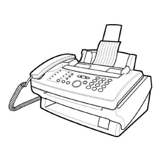
- Page 12 1.3 General Appearance 1.3.1 Appearance 1.3.2 Show the operation panel...
- Page 13 1.4 General Maintenance Function Self-diagnosis (1) ROM VERSION (2) PRINT TEST (3) CHKSUM DISPLY (4) LED TEST (5) KEY TEST (6) LCD TEST (7) SENSOR TEST (8) CCD Calibration...
- Page 14 2. INSTALLATIONS 2.1 General The following flowchart outlines the installation procedure. Site selection (see 2.2) Unpacking (see 2.3) Check of contents (see 2.4) Installation of attachments (see 2.5) Initial setting...
-
Page 15: Installations
2.2 Site Selection The installation site Shall be free from outside vibrations, dust, etc. Shall not be directly exposed to sunlight and sudden changes in temperature. Must be horizontal and flat. Should have enough space in front of FAX machine to allow recording paper and documents to be stacked;... -
Page 16: Check Of Contents
2.4 Check of Contents After having taken out the machine and accompanied accessories from the cardboard box, check the contents according to the following list: (1) FAX machine (2) Handset and Spring cord (3) Documents Support (4) AC cord (5) Line cord (6) User manual (7) Ink Cartridge and SIM Card 2.5 Installation of Attachments... -
Page 17: Ac Cord Connection
J After power on, the LCD will display the INITIALIZING for a period of time. This time is used to clean the cartridge and warm up the printer.Insert the paper tray by holding it in an upright position, 2.5.3 AC Cord Connection (1) The power supply is provided as follows: Voltage range 220~240 VAC, 50/60 HZ ±... -
Page 18: Loading Paper
2.5.4 Loading Paper (1) Pull out the paper support. (2) Push the lever on the right side of paper cassette backward. Place the paper in the cassette so that the side you want to print on faces you and the top of the page points downward. -
Page 19: Routine Inspection
3. MAINTENANCE 3.1 Routine Inspection Basically, the routine inspection of following items are performed about every one year after the machine is installed. The description of routine inspection is shown in table 4.1.1. Table 3-1 Routine Inspection Inspection Item Procedure Remarks I.S Platen Clean with ethyl alcohol. -
Page 20: Stop]>
4. SYSTEM TEST TURN ON THE POWER POWER ON AND PRESS FUNCTION KEY AT THE SAME TIME <[FUNCTION]> PRESS AND HOLD 2 SEC <[STOP]> SYSTEM TEST PRESS 54188 CODE ERROR CODE CORRECT SERVICE SET <[START]> 8.1.1 <[ ]> <[STOP]> <[ ]>... - Page 21 =D/M/12H 8.1.1 CLOCK FORMAT <[ ]> CHANGE DISPLAY (M/D/12H)/ (D/M/24H)/ (M/D/24H) <[START]> 8.1.2 UPADATE <[START]> 8.1.11 <[ ]> 8.1.1 <[STOP]> <[STOP]> <[ ]> <[ ]> 8.1.2 =9600 XMT MODEM SPEED <[ ]> CHANGE SPEED (7200) / (4800)/(2400) <[START]> 8.1.3 UPADATE <[START]>...
- Page 22 8.1.5 DIAL TONE CHECK <[START]> =ON PBX/ON PSTN <[ ]> CHANGE COMBINATION 8.1.6 UPADATE <[START]> <[ ]> 8.1.4 8.1.5 <[STOP]> <[STOP]> <[ ]> <[ ]> 8.1.6 BUSY TONE CHECK <[START]> =ON PBX/ON PSTN CHANGE COMBINATION <[ ]> 8.1.7 UPADATE <[START]> <[STOP]>...
- Page 23 8.1.9 INT'L DIAL TONE <[START]> <[ ]> CHANGE DISPLAY (ON) / (OFF) 8.1.10 UPADATE <[START]> <[ ]> 8.1.8 8.1.9 <[STOP]> <[STOP]> <[ ]> <[ ]> 8.1.10 T.30 MONITOR <[ ]> CHANGE DISPLAY (ON) / (OFF) <[START]> UPADATE <[START]> 8.1.11 <[STOP]> <[STOP]>...
- Page 24 8.2.1 PRT SERVICE LIST PRINT SERVICE LIST 8.2.2 <[START]> <[STOP]> <[ ]> <[ ]> PRT TEST PATTERN 8.2.2 <[START]> PRINT TEST PATTERN 8.2.1 <[STOP]>...
- Page 25 8.3.1 SCANNER TEST <[START]> ROATE SCANNER MOTOR 8.3.2 5SEC THEN STOP 8.3.8 <[ ]> <[ ]> <[ ]> <[STOP]> 8.3.2 PRINTER TEST ROATE PRINTER MOTOR 8.3.3 <[START]> 5SEC THEN STOP <[STOP]> <[ ]> <[ ]> TX TONE 1100 HZ <[START]> XMTTING 1100HZ <[STOP]>...
- Page 26 SENSOR TEST P, D1, D2, C =XXXX SENSOR TEST END 8.3.4 <[START]> <[STOP]> 8.3.5 P=PAPER SENSOR <[ ]> 8.3.3 D1=DOC SENSOR 1 D2=DOC SENSOR 2 C=COVER SENSOR <[ ]> <[ ]> <[STOP]> X=0 OR 1 KEY TEST 8.3.5 <[START]> PLEASE ENTER KEY PRESSED ANY KEY IN <[STOP]>...
- Page 27 RESET USER OPTION 8.4.1 USER OPTION <[START]> 8.4.2 TO DEFAULT VALUE <[ ]> 8.4.4 <[ ]> <[ ]> <[STOP]> RESET SERVICE OPTION 8.4.3 8.4.2 SERVICE OPTION <[START]> TO DEFAULT VALUE <[STOP]> <[ ]> <[ ]> INITIALEZE DRAM 8.4.4 8.4.3 DRAM <[START]>...
-
Page 28: General
5. MECHANICAL DISASSEMBLY AND REASSEMBLY This chapter explains the procedures for replacement of parts, assembles and units in the field. 5.1 General 5.1.1 PRECAUTIONS PARTS REPLACEMENT (1) Before starting disassembly and re-assembly, always turn the AC power switch OFF, and pull out the AC plug. - Page 29 5.2 General Mechanical Structure The general mechanical structure of the FAX machine is shown:...
-
Page 30: How To Disassemble And Reassemble
3) The directions of Clockwise and Counterclockwise are defined viewing from the right of machine. 5.3.1 Installing the Ink Cartridge and SIM Card You can buy replacement mono cartridges from all OKI shops, main electrical retailers and good stationers. Black (item code) 1) After lifting the handset , please open the operational panel directly. - Page 31 ¡ ° Note: Put a softer plate on table to avoid operation panel to be scratched is necessary. 1) Face the bottom of machine, loosen 2 pieces of M3X8 tapping screws then open Bottom Plate Asm. from Bottom Cover. 2) Bottom Plate Asm. Pull out all connectors on Main Board, NCU Board and Power Board , then Bottom Plate Asm.
-
Page 32: Scanner Unit
pulled out from Printer Mode Unit then both units can be separated. (3) Loosen 3 pieces of M3X8 tapping screws that fix Lower Frame and Upper Cover Unit then Scanner Mode Asm. and Upper Cover Unit can be separated. 5.3.6 Scanner Mode Asm. Scanner Unit OP Unit Figure 5-4 Scanner Mode Asm. - Page 33 (3) Loosen 1 piece of M2.6X5 tapping screw on right side for fix Cover Switch Sensor then move Cover Switch Sensor. (4) I.S. Platen Asesmbly ¬ Face white I.S. Platen Asm., Gear is located on left side. With a straight screwdriver, pull upward the snap of bushings( green )at the left and right ends of I.S.
- Page 34 5.3.10 Document Guide Assembly (1) Use a straight screwdriver to separate Operational Panel and Doc. Guide Asm. (2) Setting Spring & Spur Gear Press downward the Setting Spring and move to longer side. Then Setting Spring and Spur Gear can be taken out at the same time. (3) DOC.
- Page 35 5.3.12 Upper Cover Unit (1) Paper Sensor assembly and Bottom Cover Release snap-in fingers of Paper Sensor Asm. by a straight screwdriver, then can separate Paper Sensor Asm. and Bottom Cover. 5.3.13 Printer Mode Unit Printer Mode Asm. Bottom Cover Unit Figure 5-7 Printer Mode Unit (1) Printer Mode Asm.
- Page 36 with a cross straight screwdriver. (3) Loosen 2 pieces of M3X12 tapping cap screw(with a Spring Washer on right side screw) on right and left side of Base Frame Unit with a cross straight screwdriver then Paper Feeder Unit and Base Frame Unit can be separated. 5.3.15 Paper Feeder Unit Figure 5-9 Paper Feeder Unit (1) Ground Spring &...
- Page 37 Pull Paper Support to highest point. Widen the gap that between Frame and Paper Support by straight screwdriver then Paper Support can be drawn out from Frame. (11) Spring-Knock Up Pull out two Springs-Knock Up from Frame-APF. (12) Linkage Face the rear of Frame-AFP, pull linkage out from snap of Frame. (13) Paper Guide-APF Face the bear of Plate, pull out the elastic snap by straight screwdriver then Paper Guide...
- Page 38 ¬ Cut Cable Tie for Fixing Cable Asm. - Loosen 2 pieces of M3×6 taptite screws, remove the motor. (5) Gear A, Gear B, Gear C Release 2 pieces of M2X6 tapping screw then Gear B(2X), GEAR A and Gear C can be taken out in sequence.
- Page 39 (3) Socket-616E Cable Asm. Release 2 snap for fixing Socket-616E Cable Asm. then it can be taken out from Bottom Cover. (4) Rubber Leg Face the bottom of Bottom Cover. Take out 4 pieces of Rubber Leg. 5-12...
-
Page 40: Circuit Description
6. CIRCUIT DESCRIPTION 6.1 Main Board Circuit The mother board version is the first version that begins mass-production and the circuit diagrams consists of 11 schematics which are described in the following sections. 6.1.1 Block Diagram The extended FAXENGINE chip set consists of an Integrated Fax Controller FC200(-M) and a modem chip (R96DFXL). - Page 41 8) Modem Interface. FC200 (-M) runs at a clock derived from modem clock. FC200 (-M) immediately handles interrupt request from modem in order to keep constant transmission flow. 9) Panel Interface. Four inputs, eight strobe outputs, and two control outputs support keys scan and LCD driver. 10) Battery and Power.
- Page 42 Input Output Pin Description Pin Name Pin No. Type Type (Note: Active low signals have an “n” pin name ending.) FCS1n Flash memory chip select or video control signal. /VIDCTL0 FCS2n Flash memory chip select or video control signal. /VIDCTL1 Printer Interface PCLK Thermal Print Head (TPH) clock or external DMAACK.
- Page 43 Input Output Pin Description Pin Name Pin No. Type Type (Note: Active low signals have an “n” pin name ending.) GPIO[9] (Hysteresis In) GPIO[9] or flash read enable signal for /FRDn NAND-type flash memory. GPIO[10]/ (Hysteresis In) GPIO[10] or SSSTAT2 SSSTAT2 (Hysteresis In) GPIO[11] or bus enable or serial port data GPIO[11]/B...
- Page 44 Table 6-2 FC200(-M) Signal Characteristics Input Signal Characteristics Input Description Hysteresis Pullup Type (V max.) (V min.) (V min.) Resistance(K ohm) CMOS input 0.3*VDD 0.7*VDD Hysteresis 0.3*VDD 0.6*VDD Hysteresis/Pull up 0.3*VDD 0.6*VDD 35-150 TTL input TTL/Pull up 35-150 CMOS input 0.3*VDD 0.7*VDD Absolute Input Range = -0.5 to VDD+0.5...
- Page 45 CMOS output, Open drain CMOS output (3X) VDD-1.5 High capacitance driver VDD-1.5 (3X) CMOS Output (4X) VDD-1.0 123XTT 1/2/3X (Tristate) output 1.6/4/6 1.6/4/6 Table 6-3 FC200 (-M) Memory Map Chip select Address (Hex) External to FC200(-M) Internal to FC200(-M) 000000-007FFF SRAM 00E000-00FBFF 00FC00-00FCFF...
- Page 46 6.1.2.1. Bus Cycle Timing The processor and external bus cycle timing is defined by bclk (an internal signal). bclk is referenced to TSTCLK which is derived by dividing SYSCLK by either 2 or 3,as shown in Figure 8.1.1.1-1 and Figure 8.1.1.1-2,respectively. bclk can be extended low (halted state) or stretched high (wait state) by external and internal conditions that are described later.
- Page 47 bclk TSTCLK Normal Cycle With 1 Wait State Bus Cycle WAITn Figure 6-2 Bus Cycle (Divide by 3) 6.1.2.2. External Bus Signal Timing External bus clock and control timing is provided in Figure 6-3. External bus data access timing is provided in Figure 6-4, and Table 6-4 provides the external bus signal timing parameters for both these figures.
- Page 48 Access with 1 Wait State Access with 0 Wait States TSTCLK A cc R EG S E L D M A A cce ss R E G SE L DM A REGDMA WAITn WRn,RDn A[19:0] Ext. CS's CS[4:3]n D[7:0] (Read) D[7:0] O U T O U T...
-
Page 49: Maintenance
Parameter Symbol Min. Max. Units REGDMA delay (DMA access) tDMD tSL+10 WAITn delay tWSD tSL+12 RDn,WRn delay RDn,WRn delay (Delay On=1) tSDD tSL+10 RDn,WRn delay(Delay On=2,3) tSDD WRn delay (Early Off) tSDE tSL+10 Address delay tSL+10 Chip Select delay tCSD tSL+12 Chip select (CSn[4:3]) delay tCGD... -
Page 50: General
registers during power down. 6.1.2.5. RESET logic and Watchdog Timer There are two power resets, battery power reset (/BATRST) and prime power reset (/PWRDWN). The battery power reset initializes battery backed-up logic when battery is first applied or changed. Prime power reset initializes all non-battery powered logic when system power is turned on. Another reset is generated by watchdog timer which guards against firmware lockup. - Page 51 Pin Name Signal Description Input Output Name Type Type GP04 Rrelay 2 General purpose input/output GP05 Rrelay 3 General purpose input/output GP06 RING_OFF General purpose input/output GP07 BREAK General purpose input/output OVD2 GND Connect to digital ground OVD2 GND Connect to digital ground Data bus line 7 Data bus line 6 Data bus line 5...
- Page 52 Pin Name Signal Description Input Output Name Type Type +5VA +5VA PWR Connect to analog +5V power GND Connect to analog OV ground +2.5 analog ground AOUT Smoothing filter output OVD1 GND Connect to digital ground No connection /IRQ1 /MIRQ Interrupt request /WRITE Write enable...
- Page 53 Pin Name Signal Description Input Output Name Type Type EYEY Serial eye pattern Y output GP21 General purpose input OVD2 GND Connect to digital ground GP20 General purpose input GP19 General purpose input Received data /RLSD Received line signal detected OVD2 GND Connect to digital ground RCV0...
- Page 54 Parameter Symbol Min. Typ. Max. Units Test Condition Output High Voltage ILOAD= -100 £ g A Type OA and OB ILOAD= -40 £ g A Type OE Output High Current -0.1 Types OD Output Low Voltage Types OA and OC ILOAD= 1.6 mA Types OB ILOAD= 0.8 mA...
-
Page 55: Network Interface
6.1.8 Memory There are 2 chips of 4 Mega bits DRAM mounted on board. SRAM of 32K bytes stores user and system data. DRAM was not backed up , SRAM is backed up by BT1. EPROM of 128K bits is installed on socket for various firmware versions are provided. - Page 56 6.3 Key Board Circuit Description The keyboard consists of following parts: (1) Dot Matrix LCD Module It has character generator and data RAM on board which provide easy interface for host FC200(- M). Its bus operation is 4-bit access. (2) LED Drivers and LEDs Three LEDs are driven by control LEDCTL via transistor Q1 and strobe by OP05, OP06 and OP07.
- Page 57 6.5.2.2. DTMF dialling Main board generates the DTMF signal and transmits the signal to J4 pin2 “TX”. 6.5.2.3. Pulse dialling Main board controls the reed relay K1 switching to generate the make and break duration. Dialling signal loop: J1àL1àJP24 (or K6)àLP1àK2àK1àR2àT1àR3àJP33àK2à JP9 (or LF1//CF1) àJP1àJP24 (or K6) àL2àJ1 6.5.3 Ringing Detection The ringing signal detection circuit includes D8, ZD5, ZD6, R11, C10 and PH1.
- Page 58 6.6.3 Ringing The ring signal is checked at pin FCI (U1 pin 21) for a valid ringing frequency. As soon as a signal is applied to the line, the internal ring frequency detector will start, provided that the signal level at FCI is above the trigger threshold (~2/3 V ).
- Page 59 6.7 Power Supply Description The Skynet Model SNP-2950 is a fanless switching mode power supply used for TATUNG PPF(TF- 300P) product. It is multi-output power supply which will be fixed in the fax. 6.7.1 Input Specification 6.7.1.1. Input Voltage The range of input voltage is from 90V AC to 264V AC, the AC rating show on the label: 100~240V 6.7.1.2.
- Page 60 6.7.3 General Feature 6.7.3.1. Efficiency The efficiency is higher than 72% while measuring at nominal line and max. load. 6.7.3.2. Hold Up Time The hold up time is longer than 16ms at 220VAC input and max. load which is measured from the end of the last charging plus to when the main output drop to 95% output voltage.
- Page 61 6.7.4.7. Shock Meet IEC 950/4.2 mechanical strength and stress relief test. 6.7.5 International Standards 6.7.5.1. Safety Standards Designed to meet the following standards : UL 1950 D3 CAS 22.2 NO.234, 950 VDE EN 60 950 NEMKO DEMKO SEMKO 6.7.5.2. EMI Standards Designed to meet the following conducted limits: CISPR22 Level “B: FCC “B”...
-
Page 62: Troubleshooting
7. TROUBLESHOOTING 7.1 LCD Fails to Display after Power On Check if J7 connector Insert anew normal Check if AC power Eliminate AC supply normal power fault Check if DC power Elininate power supply normal supply fault Check if key board plug loose... - Page 63 7.2 Half of LCD Display Full Black after Power On Check if U11(ROM) Inser anew inserted normally Check if Clock of Check if X2(Crystal) Solder anew or FC-200 U1 133 is 12 R180, C98, C99 normal replace Check U24--67 modem Check U24-70 reset normal hign is 12 MHz...
- Page 64 7.3 LCD Display Normal on Starting but Key Failed Make sure the soldering state of U1- 38~52 are normal Check if there is output Soler anew Check soldering of U1 signal in U1-57 Replace U1 Check soldering of Check if there is output signal in U136-144 Check U1-52 while Check soldering of...
- Page 65 7.4 Time Display Abnormal Power On Check BT1 > 4.0V Power Off Replace Battery or Check if the voltage of battery charging D27-2 > 2.25V Check X1, C6, C7,...
- Page 66 7.5 It Works Pressing Key but Speaker Remains Mute Press [DIR] key and check if there is singnal Solder anew U1 in U1-119 Check U25-3 if there is Check R268, C112 signal output Check U25-5 if there is Check U25 singnal output Check J8 on Main Board Check Speaker...
- Page 67 7.6 Reset on Starting Check if U28 soldering solder anew Check if U28-1 is Check if R57, D17 high (4.4V) normal Check soldering state of U1-62...
- Page 68 7.7 LCD Display “NO PAPER” while Recording Paper is Loaded Check if there is broken Check if J10 connector wire or incorrect Solder anew loose connection of paper sensor Insert anew Check J10-3 it should be Check sensor low while paper loaded Check U1-73...
- Page 69 7.8 C.I.S. Motor Remains Motionless Check if connectior connected properly Check if motor stuck when Check if 24V voltage Power supply circuit it is turned manually normal defective Driving IC U7 Are the signals to driving check soldering of defective IC U7-1, 2, 3, 4 normal U1-103~106 Check stepping...
- Page 70 7.9 Failed to Feed Document Check if there is a sound of beep in speaker on Check DOC. sensor document feeding circuit Check J7-17 is low (OV) Check U1-78 is low (OV) Check CIS motor driving circuit Check if J7-17 low while Check sensor sensor is triggered Check cable...
- Page 71 7.11 Copy Quality is Too Bright Check if D9, D10 Check U3-7 white level > Check U3 connected inversely 3.3V Check U1-67, 71 Solder anew 7.12 Failed to Transmit Successfully Check the Check U24-46, 22 oscillctor normal circuit Modem defectiv Check if U24-67 high Check if U24--54 active Power supply circuit...
- Page 72 7.13 Failed to Receive Successfully Check if there is signal in Check if there is signla in Check if it is 1 volt in J4-1 while receiving NCU circuit fault U23-7 U23-6 message Check R177, R178, To receive anew and Check if there is signal in Transmission circuit check transmission...
- Page 73 7.15 Printer Acts Failed Check if J1 connector Check printer loose interface Insert anew power supply is nromal 7.16 Certain Blocks Failed in Printing Check if J1-1, 2, 3, 4, 6, Check if U1-101, 102, 8 has signals during 103, 114, 115 soldered Soler anew printing actually...
- Page 74 7.17 Copy All Black Insert a white paper to do calibration Check the soldering Copy again and check if state of U17, U3 are Solder anew normal Check if J3-10=24V Check printer board when "ISON" is hign Check if Q1-B pin = 0.7V Check U1-86 Check if Q1-C, E pin Check Q1...
- Page 75 7.18 All White Printing Check if there is the Check if J1 connector Check printer broken wire in J1 falls out interface Jumpering or change Solder anew a new 7.19 Printing or Copying Error Data Check J1 inserted right J1 side Check R336, 337, 338 Check J1 soldered soldered actually...
- Page 76 7.20 Printer Can’t Initial Check solding state Refer to printer board circuit of J7 Check if power supply Check if U18-64 16MHz Check Y1 normal Check cable connect Check soldering of to printer board is U18, U19, U20 right direction 7-15...
- Page 77 7.21 Carriage Motor Remains Motionless Refer to printer board circuit Check if carrier home Inser anew sensor loose Check if 24V of U14-10 Check printer board normal Check U14 Check power supply Check if there is broken wire in J1, and J2 Solder anew Check if J3 connector Insert anew...
- Page 78 7.22 Line Feed Motor Remains Motionless Refer to printer board circuit Check if 19V Check if sensor loose of U13-9 normal Check if J4 connector Insert anew loose Check power supply Check if U13 soldered Solder anew actually Check if D5 normal Solder anew Check solder state of U10-9, 8, 14...
- Page 79 7.24 SIMCARD Invalid Check if SIMCARD Insert anew normal Check SIMcard direction Check if J9 insert normal Insert anew error Check solder state of Change it direction Check solder state of U2 Check SIMcard board 7-18...
- Page 80 7.25 Trouble Shooting Fax Mechanical Problem PROBLEM CAUSE ACTION DOC. SKEW 1. DOCUMENT WITHOUT USING 1. ADVISE THE OPERATOR TO LOAD GUIDES. DOCUMENT WITH DOCUMENT GUIDE. 2. ADF ROLLER ASM IS LOCKED 2. REPLACE CLUTCH SPRING 3. I.S. DEFORMED, I.S.’S SURFACE IS 3.
- Page 81 PROBLEM CAUSE ACTION 3. PAPER FEED GEAR DO NOT TURN. 3. REPLACE THE MOTOR OR DRIVE TRAIN ASM. 4. THE PICK ROLLER FOR WEAR. 4. REPLACE AUTO PAPER FEEDER (A.P.F UNIT). 5. PAPER PATH FOR 5. CLEAR THE PAPER PATH. OBSTRUCTIONS.
- Page 82 PROBLEM CAUSE ACTION HORIZONTAL BREAK 1. ONE OR MORE NOZZLES ARE NOT 1. RESEAT THE PRINTHEAD CABLES LINE WORKING. PROPERLY OR WIPE THE NOZZLES AND CONTACTS WITH A DAMPLY CLEAN CLOTH. 2. THE CONTACT OF PRINTHEAD 2. USE CLEAN DRY CLOTH TO CABLE IS DIRT OR WORN.
- Page 83 PROBLEM CAUSE ACTION 2. DATA DISORDER. 2. SYSTEM INITIAL AGAIN OR DISCHARGE BATTERY. 3. SRAM OF MAIN BOARD DISORDER. 3. DISCHARGE SRAM AGAIN. 4. KEY BOARD FAILED. 4. REPLACE KEY BOARD. 5. MAIN BOARD FAILED. 5. REPLACE MAIN BOARD. LCD DISPLAYED “NO 1.
- Page 84 à Check the status of C24, C25, C26, R32, R34, L11 and L12. à Check the Microphone inside handset. 7-23...
- Page 85 8. PART LIST 8.1 Main Board Part List TF-300P P/N:0482325010(0.5) P/N:0482325010A(0.5) TTIC PART NO DESCRIPTION SIZE SYMBOL 0482300381 INDUCTOR SBT-0260T L11,14 £ v T YPE JUMP WIRE 0482300577 D:0.6/P:5/10/10mm L4,6 0482302508 CONNECTOR IL-S-10P-S2T2-EF 0482302636 CONNECTOR 06FM-1.0BT 0482302784 PIN HEADER 2028P18VU00...
- Page 86 TTIC PART NO DESCRIPTION SIZE SYMBOL 5195210302 SMD RESISTOR 1/10W,10K,J,0805 24 R2,9,36,50,57,58,64, 104~107,109,110,152, 153,166,167,181,193, 208,264,319,324,334 5195210402 SMD RESISTOR 1/10W,100K,J,0805 R49,74 5195210502 SMD RESISTOR 1/10W,1M,J,0805 R268 5195210602 SMD RESISTOR 1/10W,10M,J,0805 5195218102 SMD RESISTOR 1/10W,180Ù,J,0805 13 R5,6,71,180,315, 325~329,331~333 5195220202 SMD RESISTOR 1/10W,2K,J,0805 R3,37,70,119,323 5195220302 SMD RESISTOR...
- Page 87 TTIC PART NO DESCRIPTION SIZE SYMBOL 23,25,34,64,66,68~70, 81~84,86,88,89,92,93, 95,97,100,103,106,115 117,120~123 6500037800 CONNECTOR 3594S08HU00 6500037900 CONNECTOR 3594S16HU00 6502026301 HEADER 5045-02A 6502027501 HEADER 5267-06A 6550103200 IC SOCKET 32PIN 6613576409 SMT SWITCHING RLS4148 18 D1,2,9,10,13,17,18, DIODE 23~25,27~32,34,35 6615404909 SMT ZENER DIODE 3.6V/0.4W(RLZ3.6B) 6615413709 SMT ZENER DIODE 5.1V/0.4W(RLZ5.1B) 6615414509...
- Page 88 8.2 Key Board Part List TF-300P KEY BOARD P.C.B ASM P/N:0482325025(0.3) TTIC PART NO DESCRIPTION SYMBOL 0482302784 HEADER 2028P18VU00 0482314503 CONNECTOR B3B-PH-K 0482314608 CONNECTOR S8B-PH-K 0482325015 KEY BOARD P.C.B TF-300P P.C.B 0482325406 FLAT CABLE K/B-LCD(14P,L=35mm) 5195210302 SMD RESISTOR 1/10W,10K,J,0805 R6~R11,R14...
- Page 89 8.3 Print Board Part List TF-300P PRINTER BOARD P.C.B ASM P/N:0482325040 (0.6) TTIC PART NO DESCRIPTION SIZE SYMBOL 0482300381 INDUCTOR SBT-0260T 0482302504 CONNECTOR IL-S-6P-S2T2-EF 0482302515 CONNECTOR IL-Y-2P-S15T2-EF 0482314606 CONNECTOR S6B-PH-K 0482314608 CONNECTOR S8B-PH-K 0482325030 PRINT BOARD TF-300P P.C.B 5193211012 SMD RESISTOR 1/10W,F,1.1K,0805...
- Page 90 IC CARD CONNECTOR XR7A-0635-2 0482302726 FLAT CABLE 06FM-1.0SP-1.9 CONNECTOR(SMD) 0482325045 SIM CARD PCB TF-300P 8.5 NCU Board Part List TF-300P TEL/NCU ASSEMBLY PART LIST PN: 0482325316 (CTR21/38) VER 0.4 TTIC PART NO DESCRIPTION SIZE SYMBOL 0482300381 CHOKE SBT-0260 L1,L2,L5,L6 0482300577...
- Page 91 TTIC PART NO DESCRIPTION SIZE SYMBOL JP27,JP30,JP31 0482302564 TRANSFOMER LB-1058-D 0482314502 CONNECTOR B2B-PH-K-WHITE 0482314504 CONNECTOR B4B-PH-K-WHITE 0482325200 TEL/NCU PCB TF-300P (VER 0.5) 5195200002 RESISTOR(SMD) 0, 0805 R4,R34 5195210102 RESISTOR(SMD) 100, 0805 5195210302 RESISTOR(SMD) 10K, 0805 R21,R51,R52 5195210402 RESISTOR(SMD) 100K, 0805 R20,R48...
- Page 92 TTIC PART NO DESCRIPTION SIZE SYMBOL 5213222110 E.C. 220u 5213510010 E.C. C19,C36 5213610910 E.C. C1,C20,C29 5213622900 E.C. 2.2u 5213647900 E.C. 4.7u 5214422900 E.C. 2.2u/250V C5,C6 5272210510 M.C. 5272233300 M.C. 0.033u 5272247410 M.C. 0.47u C10,C12 5285415002 CAPACITOR(SMD) 5286510302 CAPACITOR(SMD) C13,C17,C24,C25,C37, 5286522302 CAPACITOR(SMD) 5286547302 CAPACITOR(SMD)
- Page 93 TTIC PART NO DESCRIPTION SIZE SYMBOL 6622100709 TRANSISTOR(SMD) 6622100809 TRANSISTOR(SMD) 6622101300 TRANSISTOR Q5,Q6,Q11 6622250800 TRANSISTOR BC546B Q2,Q4 6622400800 TRANSISTOR TIP48 Q1,Q3 6624260200 TRANSISTOR(SMD) 8550 6640150500 PHOTOCOUPLER PC817 PH1,PH4 6640402800 CURRENT SENSOR MA91000045 6646202019 BILATERAL SWITCH TC7S66F 6655006000 TELPHONE IC AS2534 6699001202 RESONATOR 3.58MHz...
- Page 94 TF-300P TEL/NCU ASSEMBLY PART LIST P.N.: 0482325312 (Germany) VER 0.4 TIC PART DESCRIPTION SIZE SYMBOL 0482300381 CHOCK STB-0260 L1,L2,L5,L6 0482300577 JUMP WIRE L9, L10,L11,L12, 0482300584 JUMP WIRE 11 JP1,JP2,JP13,JP15,JP 18,JP23,JP24,JP26,JP 27,JP30,JP31 0482302565 TRANSFOMER TA12002N 0482314502 CONNECTOR B2B-PH-K-WHITE 0482314504 CONNECTOR B4B-PH-K-WHITE...
- Page 95 TIC PART DESCRIPTION SIZE SYMBOL 5195247302 RESISTOR(SMD) 47K, 0805 R12,R13,R38 5195262102 RESISTOR(SMD) 620, 0805 5195262202 RESISTOR(SMD) 6.2K, 0805 5195275202 RESISTOR(SMD) 7K5, 0805 5195275302 RESISTOR(SMD) 75K, 0805 5195333004 RESISTOR(SMD) 33, 1206 5195382004 RESISTOR(SMD) 82,1206 R2,R3 5213210110 E.C. 100u C27,C31 5213222110 E.C. 220u 5213510010 E.C.
- Page 96 TIC PART DESCRIPTION SIZE SYMBOL 6612575200 DIODE 1N60 D9,D10 6613576409 DIODE(SMD) 1N4148 D1,D2,D3,D16,D17 6615406109 ZENER DIODE(SMD) 6615406209 ZENER DIODE(SMD) 6615406609 ZENER DIODE(SMD) ZD11 6615413709 ZENER DIODE(SMD) 5.1V ZD1,ZD2,ZD5,ZD6,ZD 6622100709 TRANSISTOR(SMD) 6622100809 TRANSISTOR(SMD) 6622101300 TRANSISTOR Q5,Q6 6624220600 TRANSISTOR(SMD) 8550 6640150500 PHOTOCOUPLER PC817 PH1,PH4 6640402800...
- Page 97 8.6 Power Supply Part List TF-300P P/N: 6930011900 Item Symbol Part No. Description 100-0652- JUMPER WIRE JUMPER 7.5mm 100-0652- JUMPER WIRE JUMPER 7.5mm 100-0752-10 JUMPER WIRE JUMPER 10mm 100-0752-12 JUMPER WIRE JUMPER 12.5mm 100-0752-15 JUMPER WIRE JUMPER 12.5mm 100-0752015 JUMPER WIRE JUMPER 15mm...
- Page 98 Item Symbol Part No. Description 202-L122- EL CAPACITOR LXF 220u 25V 202-L133- EL CAPACITOR LXF 330u 25V 202-L133- EL CAPACITOR LXF 330u 25V 203-L056- EL CAPACITOR LXF 56u 35V 203-L139- EL CAPACITOR LXF 390u 35V 203-L139- EL CAPACITOR LXF 390u 35V 205-F010- EL CAPACITOR KMF 10u 50V 205-F010-...
- Page 99 Item Symbol Part No. Description 500-2843- TRANSISTOR 699-7912- 699-7912- 699-C123- 699-L431- 710-9908-L PIN HEADER 710-LS02- PIN HEADER 710-PH06- PIN HEADER 8-15...
- Page 100 9. MECHENICAL DRAWING AND PARTS LIST...
- Page 109 9-10...
- Page 110 9-11...
- Page 111 9-12...
- Page 112 9-13...
- Page 113 9-14...
- Page 114 9-15...
- Page 115 9-16...
- Page 116 10. CIRCUIT DRAWING 10-1...
- Page 117 10-2...
- Page 118 10-3...
- Page 119 10-4...
- Page 120 10-5...
- Page 121 10-6...
- Page 122 10-7...
- Page 123 10-8...
- Page 124 10-9...
- Page 125 10-10...
- Page 126 10-11...
- Page 127 10-12...
- Page 128 10-13...
- Page 129 10-14...
- Page 130 10-15...
- Page 131 10-16...
- Page 132 10-17...
- Page 133 10-18...
- Page 134 10-19...
- Page 135 10-20...
- Page 136 10-21...
- Page 137 10-22...
Need help?
Do you have a question about the TF-300P and is the answer not in the manual?
Questions and answers