Oki OKIFAX 5650 Maintenance Manual
Hide thumbs
Also See for OKIFAX 5650:
- User manual (251 pages) ,
- Options manual (12 pages) ,
- User manual (138 pages)
Table of Contents
Troubleshooting

Subscribe to Our Youtube Channel
Related Manuals for Oki OKIFAX 5650


Summary of Contents for Oki OKIFAX 5650
- Page 1 OKIFAX 5650 Maintenance Manual First Edition Note: Throughout this manual there are many references to the G4/ ISDN option. This option is not available in the U.S. or CANADA. January, 2001 Oki Data Corporation...
- Page 3 PREFACE This manual is intended to be used for installing and maintaining OKIFAX 5650 facsimile trans- ceiver. Maintenance of the OKIFAX 5650 is assumed to be conducted at the following levels: • Assembly-level maintenance for mechanical portions • Unit-level maintenance for electrical at portions CAUTION: DANGER OF EXPLOSION IF BATTERY IS INCORRECTLY REPLACED.
-
Page 4: Table Of Contents
CONTENTS GENERAL INFORMATION ................7 General Performance ...................... 7 General User’s Function ....................10 General Maintenance Functions ..................13 General Appearance ....................... 14 Basic Performance Specifications ................... 16 Reports and Lists ......................26 Configuration ........................47 1.7.1 Print conditions ....................47 1.7.2 Report image ....................... - Page 5 6.13 Protocol Dump Data Printing ................... 215 6.14 System Reset ........................219 6.15 Service Code ........................220 TROUBLESHOOTING AND REPAIR FOR OKIFAX 5650 ......235 Overall Troubleshooting Flow Chart ................237 No LCD Operation ......................238 ALARM LED On ......................239 Printing Test Failure ......................
- Page 6 APPENDIX F SECOND PAPER FEEDER MAINTENANCE MANUAL ....450 OF5650 January 2001...
-
Page 7: General Information
• 128 mm to 356 mm Length setting : Unlimited (1500 mm) is also available. (7) Automatic document feeder (ADF) • 30 sheets (NA Letter/A4-size: 20-lb/75gm Oki Data recommended paper) • 15 sheets (NA Letter/A4-size: 13 to 28-lb/49 to 105gm) Note: NA is North America (8) Recording paper or sheet •... - Page 8 (12) Scanning resolution a) Horizontal : • 300 dots/inch b) Vertical : Transmission mode : 3.85 line/mm (STD), 7.7 line/mm (FINE), 15.4 line/mm (EX.FINE) or 300 dot/inch (EX.FINE) COPY mode : 7.7 line/ mm(FINE) or 300 dot/inch(EX.FINE) 300 dpi ¥ 300 dpi (Transmission is available.) Note : (13) Scanning method •...
- Page 9 PC Printer Function PC Scanner Function PC FaxModem Function Note: For details, see “OKIFAX 5650 Product Specification for MFP” Hardware is standard and software is option for Bi-Centro interface. (29) Fax2Net : Provider type (option) The following functions are available.
-
Page 10: General User's Function
General User’s Function (1) Transmit mode • Automatic transmit mode • Manual transmit mode (2) Receive mode • Automatic receive mode • Manual receive mode • TEL/FAX automatic switchover mode • TAD mode • Memory only receive mode • Forwarding mode •... - Page 11 (20) Confidential message reception • 16 mail boxes (21) PHOTO mode (Half-tone transmission) • 64 scale gradations (22) G3 sequential broadcast (Memory) • Broadcast mode 200 stations at maximum • Delayed broadcast mode (23) No paper/no toner reception (Memory) (24) Memory-only reception (Memory reception even if paper does not run out) (25) Distinguishing Text from picture (26) Page re-transmission (Only in case of memory TX mode)
- Page 12 (43) Quick scanning 3 sec. minimum Æ A4 size 3.85 (44) Time and date setting (45) PC interface (option) • Standard: ODA version • Option: INT'L version (46) Language selection • 2 languages (LCD and Reports) (47) Fax fowarding (48) 4 digit indication of YEAR (49) Memory password programming (50) Fax network programming (51) Fax2Net service...
-
Page 13: General Maintenance Functions
General Maintenance Functions 1) Local tests (1) Self-diagnosis • CPU ROM/RAM check • FLASH (/MASK) memory check (Program, Language, Default) • Modem version • RAM check • RAM check (MEMORY board: option) • PC-IF board (parallel) check • ISDN board (option) : CPU ROM/RAM check •... -
Page 14: General Appearance
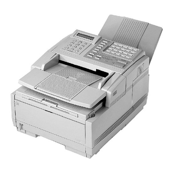
General Appearance Figure 1.1 shows the general appearance. Figure 1.2 shows the control panel. Control Panel Document Stacker One-Touch Keypad Document Guides Document Tray Sub-Paper Tray Manual Paper Feeder Cover AC Switch Recording Paper Cassette Telephone Handset (Option) Figure 1.1 General Appearance OF5650 January 2001... - Page 15 Figure 1.2 Control Panel OF5650 January 2001...
-
Page 16: Basic Performance Specifications
Basic Performance Specifications Table 1.1 shows basic performance specifications. Note: TF: Technical function setting Function program setting One-touch key pressed SELECT FUNCTION key pressed Table 1.1 (1/10) Basic Performance Specifications Item Specifications Applicable line 1) Public switched telephone network (PSTN) 2) Private branch exchange (PBX) (OT9+2) 3) Integrated services digital network (ISDN) : option Line interface... - Page 17 Table 1.1 (2/10) Basic Performance Specifications Item Specifications Effective reading width Communication Effective reading Document width Copy size Mode/Paper width width ISO A4 (210 mm) 208 mm for TX G3/A4 202.8 mm for local copy [INT’L/FTZ] NA letter (216 mm) 215.1 mm for TX G3/A4 Letter...
- Page 18 3) Weight, thickness and condition: Same as above Note: One single sheet only should be loaded on the manual loading feeder for any one occasion. For best results use Oki Data recommended papers 1) Xerox 4200 (20 - lb/75gm weight paper) 2) L-type paper for photo-printers...
- Page 19 This table does not include vertical and horizontal addressing error +/- 3 mm) of recording paper. Copy stacking The fax can discharge printed copies and stack them face- down. Maximum sheets on the copy stacker: 100* *Note : Oki Data recommended paper, New standard 20-lb. (Xerox 4200) OF5650 January 2001...
- Page 20 Table 1.1 (5/10) Basic Performance Specifications Item Specifications Scanning resolution Horizontal: • 300 dot/inch Vertical: Transmission mode: • 3.85 line/mm (STD), 7.7 line/mm (FINE), 15.4 line/mm (EX.FINE) or 300 dot/inch,(EX. FINE) Note: 300 dpi ¥ 300 dpi ; Transmission is available COPY mode: 7.7 line/ mm (FINE) or 300 dot/inch (EX.
- Page 21 Specifications Minimum scan line time for receiv- 0 ms, when receiving in ECM mode or from an Oki Data facsimile. 5 ms at 15.4 line/mm or 7.7 line/mm and 10 ms at 3.85 line/mm when receiving from a non-Oki Data facsimile or non-ECM mode.
- Page 22 Item Specifications Protocol 1) ITU-T Rec. T.30 2) Oki Data special protocol High-speed protocol The T.30 protocol signal from the transmitting station is sent at message transmission speed instead of 300 bps. Note: In high-speed protocol, V.34 is not applied.
- Page 23 1) PC local printer function 2) PC scanner function 3) PC FaxModem function Note: This function will be supplied as the OKIFAX 5650 option in case Oki Data can get the approval in respective countries without modifying the optional unit.
- Page 24 Table 1.1 (9/10) Basic Performance Specifications Item Specifications ISDN G4 (Option) The following four modes are supplied. 1) G4 function 2) ISDN G4 communication 3) ISDN G3 communication 4) ISDN report and list Note: For details, see Appendix H “ISDN G4 option system specifications”...
- Page 25 Table 1.1 (10/10) Basic Performance Specifications Item Specifications Weight Approx. 13 kg (Main body) Excluding optional units, recording paper and packing mate- rials. 1) AC power cord ¥ 1 Attachment 2) I/D unit ¥ 1 (Already installed) (to the main body) 3) Toner cartridge ¥...
-
Page 26: Reports And Lists
Reports and Lists Table 1.2 shows Reports and Lists Specifications. Note: F +OT: Press FUNCTION and One-touch key Function program setting Technical function setting Table 1.2 (1/2) Reports and Lists Specifications Item Specifications Call-back message The transmitter sends a call-back message to the receiver only when the receiver does not respond to voice request of the transmitter. - Page 27 Table 1.2 (2/2) Reports and Lists Specifications Item Specifications Confidential reception report The fax can print out this report automatically on completion of a confidential reception. Telephone directory This directory is printed manually. (REPORT PRINTING +3) Configuration report This report is printed manually. (REPORT PRINTING +4) Active memory files This report will be manually or automatically printed out for...
- Page 28 (2) Sender ID (3) CSI/Personal ID (4) Letters "PLEASE CALL BACK" (5) Sender ID (6) Sender’s call back telephone number Sender ID Format: (Example) OKI ABC 1234 → 3454 2000 07/01/1999 15:06 NO.021 (1) Date and time (2) Sender ID (3) Receiver’s CSI/Personal ID...
-
Page 29: Power Outage Report
S,R-TIME DISTANT STATION ID MODE PAGES RESULT 06/30 10:10 0485-88-3385 LOST 9080 06/30 10:30 ODS TAKASAKI LOST 0000 06/30 12:05 01'20" OKI FAX CONF=01 LOST 0000 06/30 13:00 00'20" 03-5476-4300 LOST 0000 06/30 10:50 01'20" 0495-22-5400 LOST 0000 06/30 15:00 B.C. -
Page 30: Activity Report
TOTAL TIME CALLING=08:22' CALLED=17:30' DATE TIME S,R-TIME DISTANT STATION ID MODE PAGES RESULT (10) (11) (12) 05/17 10:00 01'20" OKI FAX CALLING 0000 05/17 10:10 01'00" 0485 88 3385 CALLING STOP 9080 05/17 10:30 00'20" ODS TAKASAKI POLLING 0000 05/17 12:05 01'20"... - Page 31 Title of the report Date and time when the report was printed Sender ID Total CALLING and CALLED time Date of transmission or reception Time when the communication started Time span of the fax communication. Identification of the remote station Personal ID/Location ID/TSI/CSI/Dial number or space Communication mode: CALLING...
-
Page 32: Message Confirmation
Message Confirmation Report Format (1/2): (Example) MESSAGE CONFIRMATION 07/01/1999 08:05 ID=OKI (10) DATE S.R-TIME DISTANT STATION ID MODE PAGES RESULT 07/01 00’20" OKI FAX CALLING 0000 OF5650 January 2001... - Page 33 MESSAGE CONFIRMATION 07/01/1999 17:05 ID=OKI (10) DATE S.R-TIME DISTANT STATION ID MODE PAGES RESULT 07/01 00’20" OKI FAX B.C. COMP 60A0 07/01/96 17:00 OKIFAX No.022 150 km (11) (1) Title of the report (2) Date and time when the report was printed...
- Page 34 BROADCAST ENTRY REPORT P1 02/14/2000 12:00 ID=ODS LOCATION ID LOCATION ID ONE TOUCH 1=12345678901234567890123456789012 2=12345678901234567890123456789012 3=OKI DATA CORP. 4=s-ishika@okidata.co.jp 5=timomo@alles.or.jp 6=0273265978 7=0273261234 8=0273267890 9=0273261447 10=0273265980 11=OT11 12=OT12 13=OT13 14=OT14 15=OT15 16=OT16 17=OT17 18=OT18 19=OT19 20=OT20 21=OT21 22=OT22 23=OT23 24=OT24 25=OT25...
- Page 35 BROADCAST ENTRY REPORT P2 02/14/2000 12:00 ID=ODS LOCATION ID LOCATION ID AUTO DIAL 095=12345678901234567890123456789012 096=12345678901234567890123456789012 097=ODS 098=OKI DATA SYSTEM 099=AD99 100=AD100 101=AD101 102=AD102 103=AD103 104=AD104 105=AD105 106=AD106 107=AD107 108=AD108 109=AD109 110=AD110 111=AD111 112=AD112 113=AD113 114=AD114 115=AD115 116=AD116 117=AD117 118=AD118 119=AD119...
-
Page 36: Broadcast Confirmation Report
= 01 START IME = 02/04 11:00 TOTAL TIME = 00:30’34" LOCATION PAGES RESULT LOCATION ID PAGES RESULT ONE TOUCH 1=123456789012345678901234 2=1234567890123456789012 3=OKI DATA CORP. 4=s-ishika@okidata.co.jp AUTO DIAL 001=12345678901234567890123 002=1234567890123456 003=ODS 004=OKI DATA SYSTEM 005=AD05 006=AD06 KEYPAD 123456789012345678901234 12345678901234567890 Max. 70-line Note: When the number of printed line exceeds Max.70-line, 2nd page is printed out. -
Page 37: Confidential Rx Report
CONFIDENTIAL RX REPORT 07/01/2000 17:05 ID=OKI DATE TIME S,R-TIME DISTANT STATION ID MODE PAGES RESULT 07/01 17:00 00'00" CONF=01 0000 Figure 1.6 Confidential RX Report OF5650 January 2001... -
Page 38: Telephone Directory
Telephone Directory 1.8.1 Print conditions OKIFAX 5650 Number of OTs Number of ADs Number of groups Maximum number of digits of OT/AD Tel No. Maximum number of digits of OT OR Tel No. Maximum number of digits of Email/Web 64 (Alphabetic small letters can be printed.) - Page 39 TELEPHONE DIRECTORY P1 02/14/2000 12:00 ID=ODS LOCATION ID TEL NO. G3-ECHO/G3-RATE/MODE ONE TOUCH ABCDEFGHIJKLMNO 1234567890123456789012345678901234567890 / 33.6K / G4 1234567890123456789012345678901234567890 123456789012345678901234567890 OFF / 9.6K / G3 12345678901234567890 / 33.6K / G4 12345678901234567890 / 33.6K / G4 12345678901234567890 / 33.6K / G4 s-ishika@okidata.cp.jp http://www.fax2net.com/ 12345678901234567890...
- Page 40 TELEPHONE DIRECTORY P2 02/14/2000 12:00 ID=ODS LOCATION ID TEL NO. G3-ECHO/G3-RATE/MODE ONE TOUCH ABCDEFGHIJKLMNO 1234567890123456789012345678901234567890 / 33.6K / G4 1234567890123456789012345678901234567890 OFF / 9.6K / G3 / 33.6K / G4 / 33.6K / G4 / 33.6K / G4 / 33.6K / G4 http://www.yahoo.co.jp/ / 33.6K / G4 http://www07.taka.okidata.co.jp/vb/install.HTM...
- Page 41 TELEPHONE DIRECTORY P3 02/14/2000 12:00 ID=ODS LOCATION ID TEL NO. G3-ECHO/G3-RATE/MODE AUTO DIAL AD46 1234567890123456789012345678901234567890 / 33.6K / G4 AD47 123456789012345678901234567890 / 33.6K / G4 AD48 12345678901234567890 / 33.6K / G4 / 33.6K / G4 / 33.6K / G4 / 33.6K / G4 / 33.6K / G4 / 33.6K / G4 / 33.6K / G4...
- Page 42 TELEPHONE DIRECTORY P4 02/14/2000 12:00 ID=ODS LOCATION ID TEL NO. G3-ECHO/G3-RATE/MODE AUTO DIAL AD111 1234567890123456789012345678901234567890 / 33.6K / G4 AD112 123456789012345678901234567890 / 33.6K / G4 AD113 12345678901234567890 / 33.6K / G4 / 33.6K / G4 / 33.6K / G4 / 33.6K / G4 / 33.6K / G4 / 33.6K / G4 / 33.6K / G4...
- Page 43 TELEPHONE DIRECTORY P5 02/14/2000 12:00 ID=ODS GROUP NUMBER = #1 #2 #3 #4 #5 <#1 ONE TOUCH> 9 10 11 12 13 14 15 16 17 18 19 20 21 22 23 24 25 26 27 28 29 30 31 32 33 34 35 36 37 38 39 40 <#1 AUTO DIAL>...
-
Page 44: Telephone Directory P6
TELEPHONE DIRECTORY P6 02/14/2000 12:00 ID=ODS GROUP NUMBER = #6 #7 #8 #9 #10 <#6 ONE TOUCH> 9 10 11 12 13 14 15 16 17 18 19 20 21 22 23 24 25 26 27 28 29 30 31 32 33 34 35 36 37 38 39 40 <#6 AUTO DIAL>... - Page 45 TELEPHONE DIRECTORY P7 02/14/2000 12:00 ID=ODS GROUP NUMBER = #11 #12 #13 #14 #15 <#11 ONE TOUCH> 9 10 11 12 13 14 15 16 17 18 19 20 21 22 23 24 25 26 27 28 29 30 31 32 33 34 35 36 37 38 39 40 <#11 AUTO DIAL>...
- Page 46 TELEPHONE DIRECTORY P8 02/14/2000 12:00 ID=ODS GROUP NUMBER = #16 #17 #18 #19 #20 <#16 ONE TOUCH> 9 10 11 12 13 14 15 16 17 18 19 20 21 22 23 24 25 26 27 28 29 30 31 32 33 34 35 36 37 38 39 40 <#16 AUTO DIAL>...
-
Page 47: Configuration
11) CALL BACK N0.: Up to 20 digits are printed. 12) FORWARDING N0.: Up to 40 digits are printed for OKIFAX 5650. 13) SERVER TEL N0.: When FAX2NET FUNCTION is set to ON, up to 40 digits are printed for OKIFAX 5650. - Page 48 20) ISDN CALLED N0.: Up to 20 digits are printed when an ISDN board is mounted. 21) Dial parameters other than REDIAL TRIES, REDIAL INTERVAL, PBX LINE, AUTO START, and DIAL PREFIX are left blank when an ISDN board is mounted and Service Bit = OFF. 22) 33: V.34 TX RETRY “ON,”...
-
Page 49: Report Image
1.7.2 Report image CONFIGURATION P1 02/14/2000 12:00 ID=ODS FUNCTION LIST 01:MCF (SINGLE-LOC.) 02:MCF (MULTI-LOC.) 03:ERR.REPORT (MCF) 04:IMAGE IN MCF 05:SENDER ID. 06:MONITOR VOLUME 07:BUZZER VOLUME 08:CLOSED NETWORK 09:TX MODE DEFAULT MIDDLE STD/NORMAL 10:T/F TIMER PRG. 11:RING RESPONSE 12:DISTINCTIVE RING 35SEC 1 RING 13:PAPER SIZE 14:USER LANGUAGE... - Page 50 CONFIGURATION P2 02/14/2000 12:00 ID=ODS DIAL PARAMETER REDIAL TRIES 3 TRY REDIAL INTERVAL 3 MIN DIAL TONE DETECT BUSY TONE DETECT MF(TONE)/DP(PULSE) PULSE DIAL RATE 10 PPS PULSE MAKE RATIO PULSE DIAL TYPE MF(TONE) DURATION 100MS PBX LINE PBX TYPE NORMAL AUTO START DIAL PREFIX...
- Page 51 CONFIGURATION P3 02/14/2000 12:00 ID=ODS FUNCTION LIST 01:SERVICE BIT 02:MONITOR CONT. 03:COUNTRY CODE 04:TIME/DATE PRINT 05:TSI PRINT 06:TAD MODE TYPE2 07:REAL TIME DIAL 08:TEL/FAX SWITCH 09:MDY/DMY TYPE2 10:LONG DOC. SCAN 11:TONE FOR ECHO 12:MH ONLY 13:H/MODEM RATE 14:T1(TX) TIMER VALUE 15:T1(RX) TIMER VALUE 33.6K 16:T2 TIMER VALUE...
-
Page 52: Active Memory Files
TIME DISTANT STATION ID MODE PAGES POLL TX 07/02 12:05 POLL RX TRANSMISSION DATE TIME DIDTANT STATION ID MODE PAGES 07/01 20:00 OKI DATA SYSTEMS 07/01 12:03 0273242117 07/01 19:00 ODC TAKASAKI Figure 1.9 Active Memory Files OF5650 January 2001... -
Page 53: Protocol Dump P1
• JM information is moved in the arrangement of CM information. • 00 is printed always since the received SID on the 2nd page is invalid. PROTOCOL DUMP P1 12/24/1998 19:00 ID=OKI TAKASAKI DATE TIME S,R-TIME DISTANT STATION ID MODE... -
Page 54: Protocol Dump P2
PROTOCOL DUMP P2 12/24/1998 19:00 ID=OKI TAKASAKI RECEIVED FRAME FF C8 01 00 73 17 22 00 00 00 00 00 00 00 00 00 00 00 00 00 00 00 00 00 00 00 00 00 00 00 00 00 00 00 00 00 00 00 00 00... -
Page 55: Self Diagnosis Repor
ID character strings of PnP device. Small letters can be printed. The maximum number of each of letters and characters shall be 45. Printing is available for OKIFAX 5650 only when option memory is mounted. (“2M.” or “4M”) Printed only when ISDN option is provided. - Page 56 LANGUAGE VERSION aaaa HASH hhhh DEFAULT VERSION aaaa HASH hhhh RAM1 RAM2 DEFAULT TYPE 03/03/2000 12:00 DEVICE ID MFG:OKI DATA CORP; MDL:FX-046FAX; DES:OKI FX-046FAX; OPT-RAM ISDN BOARD CPU-ROM VERSION aaaa HASH hhhh CPU-RAM PROGRAM VERSION aaaa HASH hhhh DPRAM Figure 1.11 Self Diagnosis...
- Page 57 G4 Protocol Dump The printing image is as follows: PROTOCOL DUMP P1 08/25/2000 19:00 ID=OKI TAKASAKI DATA TIME S,R-TIME DISTANT STATION ID MODE PAGES RESULT 04/19 14:49 00’07" OKI SHIBAURA(6412) TX-G4 0000 Dch. SETUP CONN-ACK +Bch+ DISC REL-C STATUS SETUP-ACK CONN +Bch+ Bch.
- Page 58 PROTOCOL DUMP P2 CR/CN 00 00 00 00 00 00 00 00 00 00 00 00 00 00 00 00 00 00 00 00 00 00 00 00 00 00 00 00 00 00 00 00 00 00 00 00 00 00 00 00 00 00 CA/CC 00 00 00 00 00 00 00 00 00 00 00 00 00 00 00 00 00 00 00 00 00 00 00 00 00 00 00 00 00 00 00 00 00 00 00 00 00 00 00 00 00 00...
- Page 59 Transmission (Except Polling TX) Table 1.3 Multiple Function Combinations for Transmissions : Combination Possible : Combination Impossible Feeder TX Instant Dialing Memory TX Single Loc. TX Broadcast TX Delayed TX Confidential TX Relay Broadcast Initiate Manual TX Chain Dialing Automatic Alternate Selecting Call Closed User Group Page Retransmit Redial if Communication Error in Memory TX...
- Page 60 Reception (Except Polling RX) Table 1.4 Multiple Function Combinations for Reception : Combination Possible : Combination Impossible Paper Reception In-between Memory Reception Memory Reception Memory Only Reception Confidential RX Closed Network TSI Print TIME/DATE Print Voice Request (Initiate) Voice Request (Reception) Manual Reception Remote Reception Handled as memory reception if the real time print is not available at the cancellation of...
- Page 61 Paper Reception Feeder TX In-between Memory Reception Memory TX Initial Memory Reception Closed Network Memory Only Reception Page Re-transmit Closed Network Redial for Memory TX (Error) TSI Print Sender ID TIME/DATE Print Voice Request (Initiate) Voice Request (Initiate) Voice Request (Reception) Voice Request (Reception) Call Back Message Manual Reception...
- Page 62 Functions Voice Voice Redial if Automatic Closed Sender ID Page Call Back Communication Alternate Request Request Stop Error in Network Retransmit Preparation Message Selecting Call (Initiate) (Reception) Communication Mode Memory TX Manual Calling Automatic Call Confidential Initiate Origination Relay Broadcast Initiate Delayed Polled Auto Reception...
- Page 63 Table 1.8 Preparation TX as Dual Access PC1 ON 2'nd 1'st Standby ON HOOK During FAX Calling During RING RESPONSE Call Reception During detection of TEL/FAX During TAD detection 1st Phase B Calling ~ Transmission Feeder TX Transmission after scanning During Scanning Memory TX Dialling and Calling...
- Page 64 User Setting Items Setting Selection Note E-INT E-GER E-FRE 0-AUS 0-NZL 0-SIN 0-HNG L-AG MCF (single-loc.) ON/OFF MCF (multi-loc.) ON/OFF ERR.REPORT (MCF.) ON/OFF IMAGE IN MCF. ON/OFF SENDER ID ON/OFF MONITOR VOLUME OFF/LOW/HIGH BUZZER VOLUME LOW/MID/HIGH CLOSED NETWORK OFF/ T/R / RX TX MODE DEFAULT STD/FINE/EX-FINE/PHOTO NORMAL/DARK/LIGHT...
- Page 65 (21) User Setting Items Setting Selection Note Factory MCF (single-loc.) ON/OFF MCF (multi-loc.) ON/OFF ERR.REPORT (MCF.) ON/OFF IMAGE IN MCF. ON/OFF SENDER ID ON/OFF MONITOR VOLUME OFF/LOW/HIGH HIGH HIGH HIGH HIGH HIGH HIGH BUZZER VOLUME LOW/MID/HIGH CLOSED NETWORK OFF/ T/R / RX TX MODE DEFAULT STD/FINE/EX-FINE/PHOTO NORMAL/DARK/LIGHT...
- Page 66 50 kinds of service codes Only ISDN opt. Installed E-XXX=OEL-XXX, O-XXX=OKI-XXX, L-XXX=LANIER-XXX Note: As for the setting of the part of mesh, Default-data does'nt exist in the Default-file. This setting has the data which are characteristic of the device.
- Page 67 50 kinds of service codes Only ISDN opt. Installed E-XXX=OEL-XXX, O-XXX=OKI-XXX, L-XXX=LANIER-XXX Note: As for the setting of the part of mesh, Default-data does’nt exist in the Default-file. This setting has the data which are characteristic of the device.
- Page 68 Table 1.11 Default Setting of Dial Parameters OF5650 January 2001...
- Page 69 Model. Description ID for Plug & Play Close Setting Items Setting Selection Note E-INT E-FRE 0-AUS 0-NZL 0-SIN 0-HNG L-AG Plug & Play ID Default 00/01/02/03/04 (21) Factory 00 - ODA, 01 - OEL, 02 - Lanier, 03 - Telenolma, 04 - OKI...
- Page 70 User Setting Item XPARA[ ] MCF (single-loc.) MCF (multi-loc.) ERR. REPORT (MCF.) IMAGE IN MCF. SENDER ID MONITOR VOLUME BUZZER VOLUME CLOSED NETWORK TX MODE DEFAULT T/F TIMER PRG. RING RESPONSE DISTINCTIVE RING 1'ST PAPER SIZE USER LANGUAGE INCOMING RING REMOTE RECEIVE MEM./FEED SWITCH POWER SAVE MODE...
- Page 71 User Setting Item XPARA[ ] SPECIAL SETTINGS CLOCK ADJUSTMENT TSI/CSI SENDER ID FORWARDING TEL No. not assign not assign for TBR21 (DT detect mask LANIER Special Settings XPARAE *1: LANIER Special Settings ("0": User setting are possible. "1": User setting are impossible.) CLOCK ADJUSTMENT TSI/CSI TIME/DATE PRINT...
-
Page 72: Installation Procedure
INSTALLATION PROCEDURE Setup Information 2.1.1 General The following flowchart outlines the installation procedure. (See 2.1.2) Site selection (See 2.1.3) Unpacking (See 2.1.4) Check of contents (See 2.1.5) Installation of attachments (See 2.1.6) AC cord connection (See 2.1.7) Telephone and line connections (See 2.1.8) Packing for shipment (See 2.2.1.1) - Page 73 (See 2.2.1.7) Dual access operations System data programming (See 2.2.1.8) TSI/sender ID included. One-touch key programming Two-digit auto dial programming Group setting (See 2.2.1.9) Dial parameter settings Programming mail box password Memory operations (See 2.2.1.10) Off-line tests (See 2.2.1.11) On-line tests (See 2.3) Installation of optional units Memory PC Board...
-
Page 74: Site Selection
2.1.2 Site Selection INSTALLATION Precautions for Installation (1) Fluctuation in line voltage • 120VAC (102V to 127V) • 230VAC (198V to 264V) (2) Room temperature 50 to 90°F (10 to 32°C) (3) Humidity 20 to 80% RH (4) Operating environment Pressure: Equivalent to altitude of 2500 m (8020 feet) and below. - Page 75 (196mm) (46mm) 11.81" 19.69" (300mm) (500mm) In case of scanning length (Max. 14 inches: 356mm) *Note 1: This space is necessary for handling the handset. (option) (page 2-3) This space is necessary for removing the recording paper cassette. This space is necessary for installing the document stacker and to allow space for the fan exhaust.
-
Page 76: Unpacking
2.1.3 Unpacking 2.1.3.1 Unpacking Procedure (1) Remove tape on the top of the carton box and open its cover. External carton box Packing tape Packing tape Carton label Figure 2.1 (1/3) Unpacking Procedure (2) Take out the accessory box from the carton box. (See Figure 2.1) (3) Take out the machine with plastic wrapper from the box. - Page 77 Accessories box Right cushion assembly Left cushion assembly (Top) (Top) Front Fixed tape Machine Left cushion assembly (Bottom) Polyethylene film Right cushion assembly (Bottom) External carton box Figure 2.1 (2/3) Unpacking Procedure OF5650 January 2001...
- Page 78 Top carton box Cushion AC power cord Cellophane tape Modular cord Polyethylene bag Polyethlene bag Toner cartridge (In damp proof bag) Document stacker Carton frame Accessories box Separation frame Packing tape Accessories box Figure 2.1 (3/3) Unpacking Procedure OF5650 January 2001...
-
Page 79: Identification Contents
After having taken out the machine and accompanied accessories from the carton box, check the contents according to the following list: Table 2.1 Contents List Item No. Name Q'ty Remarks OKIFAX 5650 facsimile AC power cord I/D unit Already installed. Toner cartridge Document stacker Line cord One touch sheet Already installed. -
Page 80: Installation Of Attachments
2.1.5 Installation of Attachments 2.1.5.1 Installation of Attachments (1) Items • Image Drum (ID) Unit (already installed) • Toner cartridge • Recording paper • Document stacker (2) Procedure Toner cartridge • Peel off the fixed tape attached to the copy stacker. •... - Page 81 • Take out the toner cartridge from the damp proof bag, shake it five or six times as shown in the illustration to eliminate the toner deflection, and peel off the seal gently. Seal Toner cartridge Figure 2.2 (3/5) Toner Cartridge Installation •...
- Page 82 • Push the blue tab forward until it stops. Toner cartridge Blue tab Figure 2.2 (5/5) Toner Cartridge Installation • Clean the toner scattered in the vicinity of the toner cartridge using a cloth moistened with cold water. Do not use hot water since it makes the toner stick there. •...
- Page 83 (3) Recording paper Note: About 250 sheets of the new paper can be set in the recording paper cassette. • Remove the paper cassette from the facsimile by pulling the cassette tab. Paper cassette Figure 2.3 (1/2) Recording Paper Cassette Installation •...
- Page 84 (4) Document stacker • Hang the document stacker onto hanging position. Hanging position Document stacker Figure 2.4 Document Stacker Installation OF5650 January 2001...
-
Page 85: Ac Cord Connection
2.1.6 AC Cord Connection The power supply is provided as follows. Nominal input voltage 120VAC (Voltage range 102 to 127VAC) Nominal input voltage 230VAC (Voltage range 198 to 250VAC) Check whether the AC voltage of your input is within the above-mentioned voltage range and if so, check that the power switch is turned OFF. -
Page 86: Telephone And Line Connections
Figure 2.5 Telephone and Line Connections 2.1.8 Packing for Shipment CAUTION: When packing the OKIFAX 5650 for shipment, REMOVE THE IMAGE DRUM AND TONER FROM THE UNIT AND SHIP SEPARATELY! Failure to do this will result in damage to the machine.” OF5650 January 2001... -
Page 87: Programming And Initial Settings
Programming and Initial Settings 2.2.1 Initial Settings 2.2.1.1 General Procedure of Key Operation Figure 2.6 shows the general procedure of key operation. (STANDBY MODE) (Press the SELECT FUNCTION key.) COPY COPY X2 SELECT FUNCTION (OT) Selection by One-touch key To technical program [Prg. - Page 88 Powered on while holding the 01: MCF. (SIGNLE-LOC.) SELECT FUNCTION key down. 02: MCF. (MULTI-LOC.) 03: ERR. REPORT (MCF.) *4 04: IMAGE IN MCF. Selection by YES/NO keys or digit (1 to 8) 05: SENDER ID 06: MONITOR VOLUME OT9: USER PROGRAMMING 07: BUZZER VOLUME 08: CLOSED NETWORK 09: TX MODE DEFAULT...
- Page 89 Powered on while holding the COPY key down. Selection by YES/NO keys or digit (1 to 5) TECHINICAL PROGRAMMING Selection by YES/NO keys or digit (1 to 8) 1: SELF DIAGNOSIS 1: LOCAL TEST 2: SENSOR CALIBRATION 9: LOOP BACK 1 3: LED TEST 10: LOOP BACK 2 4: TONE SEND TEST...
- Page 90 Note: When the machine is in POWER SAVE MODE, the machine returns to standby mode by pressing the START key. *1: In case of Germany, Austria and Switzerland version, ACTIVITY REPORT message does not appear on the LCD display. *2: User can read no. of counter in LCD but can not clear. *3: User can not select in some countries.
- Page 91 2.2.1.2 Technical Functions This section explains setting items generally conducted by service personnel, not by users. Table 2.2 shows the initial setting items and their purposes. (The default setting is different by the individual countries.) Each item can be accessed by entering the corresponding service number on Technical Function.
- Page 92 Table 2.2 (1/8) Service Personnel Initial Settings T.F. Item Specifications Default Service bit Switching serviceman/user operation. ON : Service personnel’s features are avail- able. OFF : Service personnel’s features are not available. To enable or disable the following functions: • Drum (Total, Print, Scan), and toner counter clear •...
- Page 93 Table 2.2 (2/8) Service Personnel Initial Settings T.F. Item Specifications Default TAD mode Switches an automatic voice message response (For external telephone to the calling station. answering device.) TAD mode is of three types (TYPE1/TYPE2/ TYPE3). OFF/TYPE1/TYPE2/TYPE3 selectable. TYPE1 means: 1.
- Page 94 Table 2.2 (3/8) Service Personnel Initial Settings T.F. Item Specifications Default Long document SCAN Switches the function of transmitting long-size document (more than 360 mm). ON : 1500 mm or 60 min. OFF : 360 mm or 60 min. Note: 60 min is transmitting time.
- Page 95 Table 2.2 (4/8) Service Personnel Initial Settings T.F. Item Specifications Default T2, timeout value T2, timeout value (layer) Registers the time duration (in seconds) for which the receiving fax detects the EOL (End Of Line) signal during phase C. The fax will discon- nect the line when EOL cannot be detected within T2.
- Page 96 Table 2.2 (5/8) Service Personnel Initial Settings T.F. Item Specifications Default Modem attenuator Adjusts the attenuation (dB) for the message send signal power level. Adjusting value is 0 to 15 dB in one dB steps. Since the maximum send signal power level (dB) of the fax is at 0 dB, you can select 0 dB to -15 dB in one dB steps for the send signal power level.
- Page 97 Table 2.2 (6/8) Service Personnel Initial Settings T.F. Item Specifications Default Strobe for LED head Setting of LED print head strobe signals (00000- 11111). Selection of strobe width in LED head. "00000" is lightest and "11111" is darkest. Note 1: When the rank marking of the new replaced LED print head (new part) is same as that of the old used LED print head (old part), you do not always have...
- Page 98 T.F. Item Specifications Default • When transmitting, even if OKI NSF signal is detected from the remote machine, the fax transmits DCS signal (The fax does not trans- mit NSC signal.) • When Remote Diag. = ON, the fax transmits NSF signal.
- Page 99 Table 2.2 (8/8) Service Personnel Initial Settings T.F. Item Specifications Default CED Send Sets to send CED or not at the time of incoming call. ON : Sending CED OFF : Not sending CED Fax2Net Function Set up whether to make Fax2Net service. ON : Enable OFF : Disable...
- Page 100 50 kinds of service codes Only ISDN opt. Installed E-XXX=OEL-XXX, O-XXX=OKI-XXX, L-XXX=LANIER-XXX Note: As for the setting of the part of mesh, Default-data does’nt exist in the Default-file. This setting has the data which are characteristic of the device.
- Page 101 It doesn't have default data with each default type. Only one kind has data as a device. G3 FALLBACK CAUSE Only ISDN opt. Installed E-XXX=OEL-XXX, O-XXX=OKI-XXX, L-XXX=LANIER-XXX Note: As for the setting of the part of mesh, Default-data does’nt exist in the Default-file. This setting has the data which are characteristic of the device.
- Page 102 (1) TEL/FAX automatic switching This function is used for the purpose of TEL/FAX automatic switching as follows. 1) If the machine detects a call with a CNG signal indicating an auto send facsimile call, it starts an automatic document receiving operation. 2) If machine detects a call without a CNG signal, machine generates the buzzer sounds as a telephone call.
- Page 103 Switch Over Time (20/35 sec) LIFT HANDSET Load document NSF, CSI, DIS Press START AUTO REC. START Button OKI TOKYO RECEIVING G3/33.6K Manual Transmission CML"OFF" 1 sec 1 sec 3.2.sec To detect CNG signal *Note 1: Ring Back Tone — 1 sec. ON, 3.2 sec. OFF 2: When you want to talk by phone, pick up handset.
- Page 104 (2) TAD mode TAD: Telephone Answering Device TAD can be connected to external telephone terminal to record your messages. TAD records your speech and switches an automatic voice message response to the calling station. Note 1: A choice of TAD mode is available by Technical Function No. 07. 2: The predetermined time is selectable between 20 or 35 sec.
- Page 105 • TAD mode flow chart In case of TYPE 2: If the fax does not detect CNG signal during working of TAD, the machine will go to standby mode. In case of TYPE 3: The fax does not detect CNG signal during 15 seconds from TAD operation starting. The fax starts CNG signal detection after 15 seconds from TAD operation.
-
Page 106: The Display Shows
2.2.1.3 Technical Functions Example Note: The fonts displayed on the LCD operation panel may differ from the fonts written this manual. (1) Service Bit Setting Purpose To enable or disable the following functions: • Drum and toner counter display (clear) •... - Page 107 (2) Technical functions Operations: The display shows: 14:14 (Standby) Press SELECT FUNCTION key. FUNCTION SELECT FUNCTION (OT) MEMORY AVAIL.=100% COPY Press COPY key twice. COPY TECH. PROGRAMMING YES(←/1-5) NO(→) ← ← Press key. 1:LOCAL TEST YES(←) NO(→/1-6) → Press key. →...
- Page 108 Table 2.4 (1/6) Technial Functions T.F. Name of Function The Display Shows Service bit → 01:SERVICE BIT Setting (Toggle) [ X ] YES(←) NO(→) → ← X: OFF Line monitor control → 02:MONITOR CONT. Setting (Toggle) [ X ] YES(←) NO(→) →...
- Page 109 Table 2.4 (2/6) Technial Functions T.F. Name of Function The Display Shows High-speed modem rate → 13:H/MODEM RATE Setting [ X ] YES(←) NO(→) → → X: 4.8k 9.6k → → 14.4k 28.8k → 33.6k T1 (TX), timeout value 14:T1(TX)TIMER VALUE (XTTO value) [ X ] YES(←) NO(→) To 15: T1(RX)
-
Page 110: Off Hook Bypass
Table 2.4 (3/6) Technial Functions T.F. The Display Shows Name of Function Error criterion 18:ERR. CRITERION [ X ] YES(←) NO(→) To 19: OFF HOOK BYPASS → X: 00 - 99% 18:ERR. CRITERION [00] ENTER 00-99 2-digit timer entered. → 18:ERR. - Page 111 Table 2.4 (4/6) Technial Functions T.F. Name of Function The Display Shows Ring duration detection time 24:RING DURA. *10 MS [ X ] YES(←) NO(→) To 25: CML TIMING → X: 10 - 99 24:RING DURA. *10 MS ] ENTER 10-99 —...
- Page 112 Table 2.4 (5/6) Technial Functions T.F. Name of Function The Display Shows ID/TSI priority → 30:ID/TSI PRIORITY Setting (Toggle) [ X ] YES(←) NO(→) → ← X: ID Toner count clear → 31:TONER COUNT CLEAR Setting (Toggle) [ X ] YES(←) NO(→) →...
- Page 113 Table 2.4 (6/6) Technial Functions T.F. Name of Function The Display Shows Note 5 G3 setup BC → 42:G3 SETUP BC Setting (Toggle) [ X ] YES(←) NO(→) → ← X: OFF Note 5 G3 Fallback cause 43:G3 FALLBACK CAUSE Note 6 [ BA01] YES(←) NO(→) →...
- Page 114 Table 2.5 G3 Fallback Object Service Code List (If G4 TX is faulty) Classification Code Description Remarks Dch layer 3 BA01 Unallocated (unassigned) number BA02 No route to specified transit network BA03 No route to destination BA06 Channel unacceptable BA07 Call awarded and being delivered in an established channel BA10 Procedure sequence error, Line disconnected during in-band procedure...
- Page 115 2.2.1.4 User’s Functions This section explains the items usually set up by general users. Table 2.6 shows the initial setting items and their purposes. Each F.P.can be accessed by entering the corresponding function number on Function Program- ming. The detailed procedure of the initial setting items will be explained on the following pages. Note: S-ON: Effective if the service bit has been set on.
- Page 116 TEL No. or Web Url is deleted. 2: Maximum number of entered digits: 64 3: When E-mail is already registered for the OKIFAX 5650, even if the account No. is deleted, the registered contents are stored. (E-mail is recovered by entering the account No.
- Page 117 3: When Web Url is registered in a one- touch in a group, the one-touch is deleted from the group destination. 4: Since the OKIFAX 5650 is already registered in Web Url, the registered con- tents are stored even if the account number is deleted.
- Page 118 Table 2.6 (3/6) User's Functions Item Specifications 4) Chain dial The number of dialling digits can be expanded to longer digit numbers by chaining any number of the above 1), 2) and 3). 5) Mixed dial Type of dialling can be changed from pulse dial to tone dial halfway in dialling process.
- Page 119 Table 2.6 (4/6) User's Functions Item Specifications 4) Search processing by the SEARCH key is performed. • OT for Tel or E-mail registration is searched in the Fax2Net enabled state. (OT for Web Url registration is not a search target.) •...
- Page 120 Table 2.6 (5/6) User's Functions Item Specifications Delayed transmission from the The fax can automatically transmit documents at 20 specified memory times from the memory. Polling transmission Document(s) placed on the feeder can be collected by a (To be polled) remote station.
-
Page 121: Specifications
Table 2.6 (6/6) User's Functions Item Specifications Dual Access Combination Table PC1 ON 2'nd 1'st Standby ON HOOK During FAX Calling During RING RESPONSE Call Reception During detection of TEL/FAX During TAD detection 1st Phase B Calling ~ Transmission Feeder TX Transmission after scanning During Scanning Memory TX... - Page 122 User's Initial Settings Note: The fonts displayed on the LCD operation panel may differ from fonts written this manual. 2)-1 One Touch Key Operations Restrict Access = ON ID NG 1 4 : 1 4 F A X POWER ON E N T E R I D →...
- Page 123 OKIFAX 5750/5950: 01 to 16 OKIOFFICE84/OKIFAX 4500: 01 to 08 OKIFAX 4550/OKIFAX4550 ISDN: 01 to 08 OKIFAX 5650 01 to 16 Relay broadcast initiate transmis- This function automatically originates a message call via sion relay key station (which must be equipped with OKIFAX 2600, OF-38, OF-27, OKIFAX 5950 or equivalent) up to 120 locations for OKIFAX 2600 and 99 locations for OF-38 or OF-27.
- Page 124 Table 2.7 (2/6) User's Initial Settings (One-touch key Program) F+OT Item Specifications Report printing The report print in 6 items are as follows: 1. Activity report 2. Broadcast message confirmation report (Multi location) 3. Activity memory files report 4. Phone directory report 5.
- Page 125 Table 2.7 (3/6) User's Initial Settings (One-touch key Program) F+OT Item Specifications Location program 1) One-touch key One-touch keys allow registering: (1) Telephone number (numeral, -, P and space) in 40 digits. (2) Alternate fax telephone number in 40 digits. (additional registration) (3) ID for the telephone directory function in 15 characters (alphabetic, numeric and symbolic).
- Page 126 1) Number of forwarding for incoming call destination that can be specified. OKIFAX 5650: 1 2) Number of characters used to specify a destination. 40 characters (numeral, -, P and Space). OF5650 January 2001...
- Page 127 Table 2.7 (5/6) User's Initial Settings (One-touch key Program) F+OT Item Specifications 7) Memory password programming Registering the password required (4-digit numerals) for outputting the data received by Memory Only Reception mode or change from Memory Only Reception mode. When the four-digit numeric password is registered.
- Page 128 Table 2.7 (6/6) User's Initial Settings (One-touch key Program) F+OT Item Specifications #. ISDN programming Sets to Country code, ISDN No. (subscriber number), ISDN ID (subscriber code) and ISDN sub address. 1) Setting values This setting consists of the following: •...
- Page 129 2)-2 Function Program Table 2.8 (1/5) User's Initial Settings (Function Program) P.F. Item Specifications Default Message confirmation report Enables or disables the automatic message (Single location) confirmation report printing after a single loca- tion call. ON : Printing the MCF report. OFF : Disables this function.
- Page 130 Table 2.8 (2/5) User's Initial Settings (Function Program) P.F. Item Specifications Default Closed network The fax compares lower four digits of TSI/CSI received from remote station with fax numbers registered locally for one-touch dial and two-digits autodial. If unmatched, the communication will be auto- matically disconnected.
- Page 131 Table 2.8 (3/5) User's Initial Settings (Function Program) P.F. Item Specifications Default User language A choice of 2 languages for LCD and print mes- sage are available. GER, FRE etc. are displayed insted of OTHER. ENGLI/OTHER selectable. Incoming ring Instead of ringer circuit, software can control built- in speaker to ring sound.
- Page 132 Table 2.8 (4/5) User's Initial Settings (Function Program) P.F. Item Specifications Default PC/FAX switch To enable or disable PC interface function. When PC reception is not available, for example, application is not activated on the PC or cable is missing between PC and fax etc., this setting allows to switch from PC to fax reception auto- matically.
- Page 133 Table 2.8 (5/5) User's Initial Settings (Function Program) P.F. Item Specifications Default Width Reduction This function can print characters written at the edges of a document. Switches the reduction of the horizontal scanning direction. ON : Reduction printing (216 mm to 203 mm) Reduction rate is shown as below.
- Page 134 User Setting Items Setting Selection Note E-INT E-GER E-FRE 0-AUS 0-NZL 0-SIN 0-HNG L-AG MCF (single-loc.) ON/OFF MCF (multi-loc.) ON/OFF ERR.REPORT (MCF.) ON/OFF IMAGE IN MCF. ON/OFF SENDER ID ON/OFF MONITOR VOLUME OFF/LOW/HIGH BUZZER VOLUME LOW/MID/HIGH CLOSED NETWORK OFF/ T/R / RX TX MODE DEFAULT STD/FINE/EX-FINE/PHOTO NORMAL/DARK/LIGHT...
- Page 135 (21) User Setting Items Setting Selection Note Factory MCF (single-loc.) ON/OFF MCF (multi-loc.) ON/OFF ERR.REPORT (MCF.) ON/OFF IMAGE IN MCF. ON/OFF SENDER ID ON/OFF HIGH HIGH HIGH MONITOR VOLUME OFF/LOW/HIGH HIGH HIGH HIGH BUZZER VOLUME LOW/MID/HIGH CLOSED NETWORK OFF/ T/R / RX TX MODE DEFAULT STD/FINE/EX-FINE/PHOTO NORMAL/DARK/LIGHT...
-
Page 136: The Display Shows
2.2.1.5 User's Functions Example Note : The fonts displayed on the LCD operation panel may differ from fonts written this manual. Function Program Operations: The display shows: To bring the LCD up to the desired message, 1:FUNC. PROGRAMMING press SELECT FUNCTION key once and ←... - Page 137 Table 2.10 (1/3) User's Functions Tap No. Name of Function The Display Shows → Message 01:MCF(SINGLE-LOC.) Setting (Toggle) confirmation report → ← X: OFF ← → ] YES( ) NO( (Single location) → Message 02:MCF (MULTI-LOC.) Setting (Toggle) confirmation report →...
- Page 138 Table 2.10 (2/3) User's Functions Tap No. Name of Function The Display Shows → User language 14:USER LANGUAGE Setting → ← X: ENG. (Other) ← → ] YES( ) NO( → Incoming ring 15:INCOMING RING Setting (Toggle) ← → ] YES( ) NO( X: OFF Remote receive...
- Page 139 Table 2.10 (3/3) User's Functions Tap No. Name of Function The Display Shows → Width reduction 27:WIDTH REDUCTION Setting (Toggle) ← → ] YES( ) NO( → ← X: OFF → Toner save 28:TONER SAVE Setting (Toggle) ← → ] YES( ) NO( →...
- Page 140 Note 1: RESOLUTION & ORIGINAL of Tx mode defult setting can be selected by using Æ key. STD / NORMAL STD / DARK STD / LIGHT FINE / NORMAL EX. FINE / NORMAL FINE / LIGHT FINE / DARK EX. FINE / DARK EX.FINE / LIGHT PHOTO / NORMAL PHOTO / DARK...
-
Page 141: Ring Response
Ring response time Before specifying the ring response time, set the service bit on following the operations shown in 2.2.1.3. (Service Bit Setting). Operations: The display shows: To bring the LCD up to the desired SELECT FUNCTION (OT) message, press SELECT FUNCTION MEMORY AVAIL.=100% key once and one-touch key No. - Page 142 Dial parameters (In case the service bit is "OFF".) To get the "DIAL PARAMETER" message on the display, perform the same operetion as Table 2.11. (Dial parammeters settings). 2:DIAL PARAMETER ← → YES( /1-9*#) ← REDIAL TRIES Available for USA, INT’L, NOR, SWE, FIN. GER, HUN, ←...
- Page 143 The following table can be set depending on the National codes even if the service bit is "off". Table 2.11 Dial parameters setting if the service bit "OFF" NATIONAL CODE USA INT’L GBR IRL NOR SWE FIN DEN GER HUN TCH POL Redial tries Redial interval Dial tone detect...
-
Page 144: Clock Adjustment
2.2.1.6 Clock Adjustment Operations: The display shows: To bring the LCD up to the desired message, SELECT FUNCTION (OT) press SELECT FUNCTION key once and MEMORY AVAIL.=100% one-touch key No. 9 in the standby mode. (In case of no message in memory) Press OT9 Enter 3 using the ten-key pad. - Page 145 2.2.1.7 Dual Access Operation OKI TOKYO OKI TOKYO OKI TOKYO SENDING /144 RECEIVING/144 MEMORY-RX/144 Set documents during memory TX Set documents Set documents or set documents during feeder TX after the end of the pre-scanning RELOAD DOCUMENT Pre-feed error SELECT LOCATION...
- Page 146 2.2.1.8 System Data Programming • TSI/CSI (Defalut: Blank) • Registration of sender ID (Defalut: Blank) • Registration of telephone number for the call-back message (Defalut: Blank) Operations: The display shows: To bring the LCD up to the desired SELECT FUNCTION (OT) message, press SELECT FUNCTION MEMORY AVAIL.=100% key once and one-touch key No.
- Page 147 Operations: The display shows: Continued from the previous page. NO=03 3404 7123 ID=OKI (Example) START Press key. START NO=<CALL BACK NO.> 3 SEC LATER NO=_ 03..5 NO=03 3404 7765_ (Example) Press START key. START OF5650 January 2001...
- Page 148 2.2.1.9 Dial Parameters Settings (1) Procedure The following shows the case in which the service bit is on. Operations: The display shows: To bring the LCD up to the desired message, SELECT FUNCTION (OT) press SELECT FUNCTION key once and MEMORY AVAIL.=100% one-touch key No.
- Page 149 The display shows: Continued from the previous page. 2:DIAL PARAMETER ← → YES( /1-9*#) ← (1) Redial time REDIAL TRIES "0 TRY" to "10 TRY", ← → [2 TRY] YES( ) NO( "1 TRY" to "5 TRY" (country code=FRE) ← →...
- Page 150 C O U N T R Y C O D E User Setting Items Setting Selection INT'L REDIAL TRIES 0 - 10 TRIES REDIAL INTERVAL 1 - 6 min DIAL TONE DETECT ON / OFF BUSY TONE DETECT ON / OFF MF (TONE)/DP (PULSE) DP / MF 10 PPS / 16 PPS /...
- Page 151 Table 2.13 Dial Parameters Settings Item Specifications Dial parameters Redial tries Switches on the re-dial times to meet the regulations of the installed country. 0 to 10 tries (in one-try steps) 1 to 5 tries for FRE. Redial interval Switches on the re-dial intervals to meet the regulations of installed country.
-
Page 152: Self-Diagnosis
2.2.1.10 Off-line Tests (1) Purpose Activate self-diagnosis which includes: • Print test • CPU-ROM version printing • CPU-RAM check • PROG version printing • LANGUAGE version printing • DEFAULT version printing • RAM check • RAM check (memory board: optional) (2) Procedure Operations: The display shows:... - Page 153 LANGUAGE VERSION aaaa HASH hhhh DEFAULT VERSION aaaa HASH hhhh RAM1 RAM2 DEFAULT TYPE 03/03/2000 12:00 DEVICE ID MFG:OKI DATA CORP; MDL:FX-046FAX; DES:OKI FX-046FAX; OPT-RAM ISDN BOARD CPU-ROM VERSION aaaa HASH hhhh CPU-RAM PROGRAM VERSION aaaa HASH hhhh DPRAM Figure 2.7 Printed Data of Self-diagnosis Print Test (Example)
- Page 154 2.2.1.11 On-line Tests Transmission (1) Load documents (2) Make sure that • The loaded documents are fed in automatically. • The STD and NORMAL lamps light. • The display shows SELECT LOCATION. (3) Dial the telephone number of the remote machine by the ten-key pad. (4) Make sure that the telephone number of the remote machine is shown on the display.
- Page 155 X X : X X X X X (STANDBY CONDITION) (• LOAD DOCUMENT(S), SELECT RESOLUTION MODE) AUTO DIALING? Manual TX WHICH MODE? ONE-TOUCH TWO-DIGIT AUTO DIAL CODE • ONE-TOUCH KEY • PRESS "AUTO DIAL" KEY (e.g. No. 1) • SET THE CODE (e.g. 01) O K I T A K A S A K I 0 2 7 3 5 6 7 8 9 0 O K I T A K A S A K I...
- Page 156 X X : X X X X X (← STANDBY CONDITION) MANUAL RECEIVE MODE OFF-HOOK AND CONVERSATION PRESS "START" KEY AUTO RECEIVE MODE? ( RINGING DETECTED) A U T O R E C . S T A R T M A N U A L R X S T A R T TSI &...
-
Page 157: Installation Of Optional Units
Installation of Optional Units Items • Memory board • PC interface board • Telephone handset • Second paper cassette unit Procedure • Turn the facsimile power switch OFF and remove the AC power cord. Note: Unplug the AC power cord from the wall outlet first and then from the facsimile. •... - Page 158 Instllation of the memory board • In OKIFAX 5650, MEM, 2 or 4MB memory board can be mounted on to the connector CN13 of M60 board. Remove Rear Cover. Remove the rear cover by remov- ing the two screws S1 and S2 .
- Page 159 Installation of CTT (PC interface) board Remove Rear Cover. Remove the rear cover by removing the two screws S1 and S2 . Rear Cover Figure 2.14 Install CTT board. First, install CTT board on to the connector CN12 of M60 board, and then tighten the two screws to the separation plate.
- Page 160 Figure 2.16 Insert the tip of a cutter or Nipper between the mold of Rear Cover and cut out it. Note: Be careful not to rotate the cutter or Nipper, since this can cause scratching on the Rear Cover. Grasp the mold of Rear Cover, and rotate it up and down until you can able to easily remove it.
- Page 161 Installation of an optional telephone set (1) Dial Mode Setting (For TEL-UK) Set the DIAL MODE slide switch on the rear side of the telephone set according to the dial mode of the connecting line. (Set to MF for UK, Norway, Denmark, Belgium and Italy) (2) Ringer Volume Setting (For TEL-UK and TEL-S)
- Page 162 (4) After installing the connection cable to the telephone set, extend the connection cable like Figure 2.19. Figure 2.19 (5) After installing the cradle assembly to the telephone set, fix the screw like Figure 2.20. (6) Install the telephone assembly on the facsimile transceiver unit.
- Page 163 (7) Connect the terminal on the other side of the connection cable formed on the rear side of the equipment (TEL1), like Figure 2.22, to the telephone set. Figure 2.22 OF5650 January 2001...
- Page 164 Second Paper Cassette Unit This item explains how to install the Second Paper Cassette Unit option. Second Paper Cassette Unit installation (1) Turn the facsimile power switch off and remove the ACpower cord. Note: Unplug the AC power cord from the wall outlet first and then from the facsimile. AC Inlet AC power cord Figure 2.23...
- Page 165 (3) Gently lower the facsimile on the Second Paper Cassette Unit. Note: Make sure that the positioning boss of the Second Paper Cassette Unit fits into the 2 holes at the bottom of the facsimile transceiver main unit. Hole Positioning boss Hole Second paper cassetle unit Figure 2.24...
- Page 166 (5) Install the Second Paper Cassette. Approximately 500 sheets of recording paper (20-Ib bond) can be loaded. Paper can be loaded up to this line. Second Paper Cassette Figure 2.26 (6) Reconnect the power cord to the wall and the facsimile, and Turn the facsimile power on.
-
Page 167: Brief Thchnical Description
Paper eject roller Paper eject Image data (Face down) board LED head Charger Exposure Toner Doctor board cartridge blade board Charging Paper path Cleaning Developing Toner selector Cleaning Developing roller roller supply roller Inlet sensor Fusing Outlet sensor Paper Paper Paper Transfer registration... -
Page 168: Fundamentals Of The Electro-Photographic Process
Fundamentals of the Electro-Photographic Process The electro-photographic process involves six sub-processes: (1) Charging (2) Exposure (3) Development (4) Transfer (5) Fusing (6) Cleaning Outline of each process is explained below. Process Illustration Description The surface of the electro-photo- graphic Image drum is uniformly charged with negative charges by applying a negative voltage to the Charge roller... - Page 169 Process Illustration Description the Image drum is attracted to the developing roller by static electricity. EP drum The recording paper is placed over the Image drum surface and a positive charge, opposite in polarity to the toner, is applied to the reverse side of the paper from the transfer roller.
-
Page 170: Actual Electro-Photographic Process
Actual Electro-photographic Process The electro-photographic process consists of six essential processes. The following Figure 3.2 provides a general description. 2 LED head Electro-photographic drum 1 Charge roller Toner 6 Cleaning roller 5 Heater roller 3 Developing roller Recording paper Back-up roller 4 Transfer roller * Process: 1 : Charging... -
Page 171: Boards And Units
Boards and Units 3.3.1 Boards and Units The following three boards, Memory board (option), Telephone interface board (option), PC interface board (option) and three units constitute facsimile transceiver machine. • Main control board MCNT: (M60_) • Network control unit board NCU: (EN9, INU)* •... - Page 172 AC Line PC Interface MEM (Option) (2MB/4MB) Battery OPE Unit CTT (Option) CN12 CN13 AC INLET Scanner Unit CN10 Battery S MOTOR Low Power Unit MPW1581 (120V) MPW1461 (230V) PSDN Line Speaker CN2 CN1 INU/EN9 CN16 ISDN Line High Power Unit ISDN (Option) R MOTOR D MOTOR...
-
Page 173: Overall Dimension And Mechanical Structure
Overall Dimension and Mechanical Structure POW board (H08) (MPW) PC-IF board (Option) HV board (M60-) MCNT board Memory board (Option) NCU board Separation rubber Pinch roller ADF roller Scan roller Sub roller Heater roller Feed roller EP drum NCU board Hopping roller Back-up roller Image sensor... -
Page 174: Mechanical Disassembly And Reassembly
MECHANICAL DISASSEMBLY AND REASSEMBLY This chapter explains the procedures for replacement of assemblies and units in the field. The section explains the procedures for replacement of parts, assemblies, and units in the field. Only the disassembly procedures are explained here. For reassembly, reverse the disassembly procedure. - Page 175 (2) Do not try to disassemble as long as the facsimile is operating normally. (3) Do not remove unnecessary parts: Try to keep disassembly to a minimum. (4) When disassembling, follow the prescribed sequence. Otherwise, parts may be damaged. (5) Since screws and small parts are likely to be lost, they should temporarily be attached to their original positions.
-
Page 176: Tools
Tools Table 4.1 shows the tools required for the replacement of parts such as circuit boards and mechanical units. Table 4.1 Tools Q’ty Remarks Service tools Philips screw driver (L) Philips screw driver (M) Philips screw driver (S) Flat screw drivers (S) Philips screw driver (S) Radio pliers Nippers... - Page 177 Start Item number for detailed description (4.3.1) (4.3.1) Open the Doc. LED Print Head Table, Stacker Cover (4.3.2) (4.3.2) (4.3.2) (4.3.2) Open the Doc. Separation Plate Font Cover, NCU Table Cover, Main Cover (4.3.2) NCU Board (4.3.2) Open the Copy Stacker (4.3.2) (4.3.2) Font Cover, NCU...
- Page 178 (4.3.4) Scan Motor (4.3.4) (4.3.5) Scan Frame Release Guide Assembly Assembly (4.3.4) Eject Roller Assembly (4.3.5) Manual Feed Assembly (4.3.5) Copy Stacker, Fusing Unit (4.3.7) Resist Motor, Drum Motor (4.3.6) (4.3.6) (4.3.6) Lower Base Motor Ass’y Back-up Roller (Resist & Drum Transfer Roller Motors) (4.3.8)
-
Page 179: 4.3.1 Led Print Head
• The detailed disassembly procedure is explained from sub-section 4.3.1 to 4.3.8. 4.3.1 LED Print Head It is used two kind of head as the LED print head. (208 mm width or 216 mm width) (1) Disassembly procedure Document Table a) Open the Document Table assembly. -
Page 180: Id Unit, Rear Cover, Ncu Cover, Main Cover, Separation Plate, Ncu Board, Modem Board
4.3.2 ID Unit, Rear Cover, NCU Cover, Main Cover, Separation Plate, NCU Board, Document Table Modem Board (1) Disassembly procedure 1) ID Unit, Rear Cover, NCU Cover, Main Cover a) Open the Document Table assembly. Stacker Cover b) Open the stack cover by removing the buttons. - Page 181 g) First, open the Main Cover from the front side, and then, remove the Main Cover by removing the Main Cover nails at both sides on the rear side. Nail (at both sides) 2) Separation Plate a) Remove the Separation Plate by removing the two screws 4.
-
Page 182: 4.3.3 Control Panel Assembly, Paper Guide (U) Assembly
4.3.3 Control Panel Assembly, Paper Guide (U) Assembly (1) Disassembly procedure 1) Control Panel Assembly and Paper Guide (U) Assembly Screw 2 Screw 2 a) First, carry out the disassembly Paper Guide U procedure up to the point of the Assembly Control Panel 4.3.2 (Main Cover, NCU Cover... - Page 183 Separation Rubber 3) Paper guide (U) Assembly a) Separation Rubber a. The Separation Rubber can be removed from the Paper Guide (U) Assembly. b) Feed Roller Feed Roller a. Remove the ground cable by removing the two screws 5. Screw 5 b.
-
Page 184: Sub-Roller, Adf Roller Assembly, Pinch Roller, Contact Image Sensor, Document Detectors (Pc1 And Pc2)
4.3.4 Sub-roller, ADF Roller Assembly, Pinch Roller, Contact Image Sensor, Docu- ment Detectors (PC1 and PC2). (1) Disassembly procedure Screw 1 1) Scanner Unit a) First, carry out the disassembly procedure up to the point of the 4.3.2 (Rear Cover and Main Cover) and 4.3.3 (Control Panel Assembly and Paper Guide (U) Assembly). - Page 185 • Turn the Scanner Frame Assembly inside out and perform the disas- sembly procedure. Sub-roller a) Remove the Bottom Plate by removing the three screws 4. ADF Roller Earth Plate 1 Assembly b) Remove the Sub-roller from the Scanner Frame. c) Remove the Earth Plate 1 from the Scanner Frame.
-
Page 186: Resist Motor, Drum Motor, Release Guide Assembly, Manual Guide Assembly, Stacker Cover, Fusing Unit
4.3.5 Resist Motor, Drum Motor, Release Guide Assembly, Manual Guide Assembly, Stacker Cover, Fusing Unit (1) Disassembly procedure • First, carry out the disassembly procedure up to the point of the Scanner Unit Assembly removal (Refer to Sub-section 4.3.4.) 1) Resist Motor and Drum Motor a) Remove the Resist Motor by removing the two screws 1. - Page 187 3) Stacker Cover a) Disconnect the flat cable. Stacker Cover b) Remove the Stacker Cover by Flat cable pressing inward the two latches on it from the two reset levers. c) Remove the Stacker Cover by spreading it from the lower base. Reset lever Reset lever 4) Fusing Unit...
-
Page 188: 4.3.6 Lower Base, Motor Assembly, Back-Up Roller, Transfer Roller
4.3.6 Lower Base, Motor Assembly, Back-up Roller, Transfer Roller (1) Disassembly procedure Screw 1 1) Lower Base, Motor Assembly Screw 3 a) First, carry out the disassembly Lower Base procedure up to the point of the Screw 2 Fusing Unit removal. (Refer to sub-item 4.3.5.) b) Disconnect the two connectors (CN3 and CN4 on the MCNT... - Page 189 c) Release the gear by unlocking Lower Base Latch the latch on the Lower Base. d) Lift the right side of the Transfer Roller and shift rightwards, then Gear pull it out from the Lower Base. Transfer Roller (2) Reassembly procedure Reverse the disassembly procedures.
-
Page 190: 4.3.7 Resist Roller, Hopping Roller, Sensor Plates
4.3.7 Resist Roller, Hopping Roller, Sensor Plates (1) Disassembly procedure 1) Resist Roller, Hopping Roller Resist Roller One-way Clutch Gear a) First, carry out the disassembly procedure up to the point of the Lower Base removal. (Refer to sub-item 4.3.6.) b) Remove the One-way Clutch Gear. - Page 191 b) Press and hold the Clutch while pushing the Toner Sensor up and out. Toner Sensor (2) Reassembly procedure Reverse the disassembly procedures. OF5650 January 2001...
-
Page 192: 4.3.8 Mcnt Board, Power Supply Unit, Contact Assembly
4.3.8 MCNT Board, Power Supply Unit, Contact Assembly (1) Disassembly procedure Screw 2 • First, carry out the disassembly procedure up to the point of the Printer Unit removal. (Refer to sub- section 4.3.6.) Note: MCNT board is shown below. MCNT Board Screw 2 1) MCNT Board... -
Page 193: Adjustments
ADJUSTMENTS Setting of LED Print Head Drive Time • Adjustment point: Technical Function No. 26. * To bring the LCD up to Technical Function, press SELECT FUNCTION key once, COPY key twice and "2" key (In case of no message in memory). Note: When the rank marking of the replaced LED print head (new part) is the same as that of the used LED print head (old part), you do not always have to set the LED print head drive time. -
Page 194: 5.2.1 Confirmation Items
5.2.1 Confirmation Items The clock frequency and power voltage of the machine are not possible to adjust in the field. However, their measurement procedures are described here for confirmation of clock frequency and each voltage. Clock Frequency • Measurement point: M60 board;... -
Page 195: 5.2.2 Measurement
5.2.2 Measurement Turn AC power OFF. Carry out the disassembly procedure up to Main Cover and Scanner Unit removal. (Refer to the Mechanical Disassembly and Reassembly in Chapter 4.2.) Connect extension cables to the M60 board. Connect the frequency counter (for clock frequency), digital voltmeter (for power voltage) and Oscilloscope (for SIG signal). - Page 196 Connector CN1—12pin (+5VSUB) CN1—7/8pin (+5VDC) CN1—10pin (+8VDC) Crystal Oscilator CN1—11pin (-8VDC) Ground Terminal CN1—15pin (+24VDC) LC1—3pin (Clock) CN1—1/2pin (+30VDC) CN18 CN11 IC20 TR17 IC16 CN16 CN15 TR12 TR19 RAM2 RAM3 BAT1 TR14 RAM1 RM11 IC14 IC19 RM10 IC18 D13 D15 TR23 CN14 TR22...
-
Page 197: Cleaning And Maintenance
CLEANING AND MAINTENANCE Replacement of Consumable Parts The user (or service personnel) is required to replace the following items as consumable parts. (1) User side Expected Use Before Reference Item No. Part name Replacement in Figure 6.1 Toner Cartrige 2500 sheets/cartrige (at 4% duty) (ITU-T document sample No.1) (For the second or later cartridge to a new I/D Unit) - Page 198 (3) Others Table 6.1 Reliability Item Specifications Document feeder Jam occurrence and misfeeds in the automatic document feeder will be less than one in 500 operations for all specified documents. Recording paper Jam occurrence in the automatic paper feeder will be less than feeder one in 1,500 operations and misfeeds will be less than one in 500 operations for all specified recording paper.
-
Page 199: Routine Inspection
Routine Inspection Basically, the routine inspection of following items is performed about half-yearly (or every one year) after the machine is installed. The description of routine inspection is shown in Table 6.2. Table 6.2 Routine Inspection Expected Use Before Reference Item Part name Replacement No. - Page 200 (7) Separation rubber (4) Pinch roller (3) Sub roller (1) Scan roller (8) LED print head (2) Feed roller (5) ADF roller (6) Image sensor Figure 6.2 Parts of Routine Inspection OF5650 January 2001...
-
Page 201: Printer Counter Display/Clear
Printer Counter Display/Clear Note: The fonts displayed on the LCD operation panel may differ from the fonts written this manual. Purpose A user can clear the image drum unit and check some of the counters (such as the print counter, scan counter) by using the ¨ key or Æ key. 2-1. -
Page 202: The Display Shows
2-2. Procedure The following shows the case when the service bit has been set OFF & TONER COUNT CLEAR = ON. Operations: The display shows: 1 4 : 1 4 F A X To bring the LCD up to the desired message, press SELECT FUNCTION key once and Press FUNCTION key. -
Page 203: Printer Counter Display/Clear
Printer Counter Display/Clear Purpose The service personnel can clear and check the following data: • Image Drum • Toner • Image Drum (Total) • Print • Scan Procedure The following shows the case when the service bit has been set ON. Operations: The display shows: To bring the LCD up to the desired message,... -
Page 204: Local Test
Local Test 6.5.1 When G4 option board is not installed 1 : L O C A L T E S T Y E S ( ← ) N O ( → / 1 - 5 ) → key or 1-5 ←... - Page 205 6.5.2 When G4 option baord is installed 1 : L O C A L T E S T Y E S ( ← ) N O ( → / 1 - 6 ) → key or 1-6 ← key Technical Programming LT-1 ←...
-
Page 206: Self-Diagnosis Test
Self-diagnosis Test Purpose To check ROMs, RAMs and printing function. Procedure (in Case of not G4 Boad) Operations: The display shows: To bring the LCD up to the desired message, TECH. PROGRAMMING press SELECT FUNCTION key once and COPY YES(←/1-5) NO(→) key twice in the standby mode. - Page 207 • Image processor LSI RAM check • Setting DEFAULT TYPE and reading clock at self diagnosis execution. The following printing differs depending on the machine type of OKIFAX 5650 and on the condition of option provided or not. “4M” is printed for OKIFAX 5650.
- Page 208 LANGUAGE VERSION aaaa HASH hhhh DEFAULT VERSION aaaa HASH hhhh RAM1 RAM2 DEFAULT TYPE 03/03/2000 12:00 DEVICE ID MFG:OKI DATA CORP; MDL:FX-046FAX; DES:OKI FX-046FAX; OPT-RAM ISDN BOARD CPU-ROM VERSION aaaa HASH hhhh CPU-RAM PROGRAM VERSION aaaa HASH hhhh DPRAM Figure 6.3 Self-diagnosis Data...
-
Page 209: Sensor Calibration Test
Sensor Calibration Test Purpose To adjust the linearity of output levels of contact image sensor. Operations: The display shows: To bring the LCD up to the desired message, TECH. PROGRAMMING press SELECT FUNCTION key once and COPY ← → YES( /1-5) key twice in the standby mode. -
Page 210: Sensor Calibration
Operations: The display shows: Continued from the previous page Enter "2". 2:SENSOR CALIBRATION ← → YES( /1-8) ← ← Press key. 2:SENSOR CALIBRATION End of prefeed PLEASE SET DOCUMENT Set white document. Load document(s). For adjustment of levels, use white plain bond paper(s) of NA Letter or A4 2:SENSOR CALIBRAION size. -
Page 211: Led Test
LEDs Test Purpose To check all LEDs on operation panel by lighting. Procedure Operations: The display shows: To bring the LCD up to the desired message, TECH. PROGRAMMING ? press SELECT FUNCTION key once and COPY ← → YES( /1-5) key twice in the standby mode. -
Page 212: Tone Send Test
Tone Send Test Purpose To send the G3 tonal frequencies to the line. Procedure Operations: The display shows: To bring the LCD up to the desired message, 1:SELF DIAGNOSIS press SELECT FUNCTION key once, COPY ← → YES( /1-8) ← key twice and key twice. -
Page 213: Mf Send Test
6.10 High-speed Modem Send Test Purpose To check the telephone line quality in combination with a remote station programmed to the high-speed modem receive test mode. Procedure Operations: The display shows: To bring the LCD up to the desired message, 1:SELF DIAGNOSIS press SELECT FUNCTION key once, COPY ←... - Page 214 TX Side RX Side 5:MODEM SEND TEST 6:MODEM REC TEST ← → YES( /1-8) ← → YES( /1-8) ← ← Press key. Press key. CML relay operates. CML relay operates. The display shows: 5:MODEM SEND TEST " Training MODEM rate The display shows: (e.g.
-
Page 215: 6.11 High-Speed Modem Receive Test
6.11 High-speed Modem Receive Test Purpose To check the telephone line quality in combination with a remote station programmed to the high-speed modem send test mode. Procedure Operations: The display shows: To bring the LCD up to the desired message, 1:SELF DIAGNOSIS press SELECT FUNCTION key once, COPY ←... -
Page 216: Mf(Tone) Send Test
6.12 MF Send Test Purpose To send the multi-frequencies of tone dialling to the line. Procedure Operations: The display shows: To bring the LCD up to the desired message, 1:SELF DIAGNOSIS press SELECT FUNCTION key once, COPY ← → YES( /1-8) ←... -
Page 217: Tone (Tel/Fax)
6.13 Tone (TEL/FAX) Purpose To check the pseudo-ring back tone of TEL/FAX automatic switching. Procedure Operations: The display shows: To bring the LCD up to the desired message, 1:SELF DIAGNOSIS press SELECT FUNCTION key once, COPY ← → YES( /1-8) ←... -
Page 218: Protocol Dump Data Printing
6.14 Protocol Dump Data Printing Purpose To analyze the transmitted/received G3 protocol signals. Procedure • Manual print-out of the last communication. (a) Manual print-out Operations: The display shows: 14:14 FAX Press SELECT FUNCTION key, provided FUNCTION (Standby) that the service bit is ON. SELECT FUNCTION (OT) MEMORY AVAIL.=100% Press one-touch key No.6... -
Page 219: System Reset
6.14.1 G3 Protocol Dump Purpose: To allow the serviceman to obtain a list of protocol signals transferred between the transmitter and receiver. Print conditions: • Modem trace information for each TX/RX is printed. (Informeation for RX is added on 2nd page.) •... - Page 220 G3 Protocol Dump Image PROTOCOL DUMP P1 12/24/1998 19:00 ID=OKI TAKASAKI DATE TIME S,R-TIME DISTANT STATION ID MODE PAGES RESULT 12/24 18:56 00'33" 123456789012345678901234 0000 PPS_MPS PPS_EOP TRANSMITTED FRAME 00 00 00 00 00 00 00 00 00 00 00 00 00 00 00 00 00 00 00 00...
- Page 221 PROTOCOL DUMP P2 12/24/1998 19:00 ID=OKI TAKASAKI RECEIVED FRAME FF C8 01 00 73 17 22 00 00 00 00 00 00 00 00 00 00 00 00 00 00 00 00 00 00 00 00 00 00 00 00 00 00 00 00 00 00 00 00 00...
- Page 222 6.14.2 Analysis from the data The printed out data permits to analyze G3 facsimile communication protocol signals between two facsimile machines. Figure 6.5 (2/2) shows the result of an analysis on the printed data referring to Figure 6.5 (1/2) (Protocol dump data). (Transmitter) (Receiver) Dialling...
- Page 223 6.14.3 FCF (Facsimile Control Field) conversion table Table 6.2 shows all FCF signals which are needed to analyze the printed out protocol dump data. Some signals have two different hexadecimal codes in accordance with the calling party or called party. Table 6.2 FCF Signals Conversion Table Abbreviation Hex.
- Page 224 6.14.4 G4 Protocol Dump Purpose: To allow the serviceman to obtain a list of protocol signals transmitter and receiver. Method: The report will be manually printed out for maintenance purpose. If it is G4, the G4 communication protocol dump is printed out. 1.
- Page 225 Protocol Dump The printing image is as follows: PROTOCOL DUMP P1 08/25/2000 19:00 ID=OKI TAKASAKI DATA TIME S,R-TIME DISTANT STATION ID MODE PAGES RESULT 04/19 14:49 00’07" OKI SHIBAURA(6412) TX-G4 0000 Dch. SETUP CONN-ACK +Bch+ DISC REL-C STATUS SETUP-ACK CONN +Bch+ Bch.
- Page 226 PROTOCOL DUMP P2 CR/CN 00 00 00 00 00 00 00 00 00 00 00 00 00 00 00 00 00 00 00 00 00 00 00 00 00 00 00 00 00 00 00 00 00 00 00 00 00 00 00 00 00 00 CA/CC 00 00 00 00 00 00 00 00 00 00 00 00 00 00 00 00 00 00 00 00 00 00 00 00 00 00 00 00 00 00 00 00 00 00 00 00 00 00 00 00 00 00...
- Page 227 6.15 System Reset Purpose To clear or initialize the following data: (a) Location data (b) Configuration data (default) Procedure Operations: The display shows: Press SELECT FUNCTION key, COPY key twice. TECH. PROGRAMMING (In case of no message in the memory) ←...
-
Page 228: Service Code
6.16 Service Codes The service code can be printed on Activity Report to recognize the result of each communication. The activity report indicates the code ”0000", should a communication terminates on normal status as a service code. The activity report indicates one of the codes of “90XX”, should a communication terminates on abnormal status, as an error code. - Page 229 6.16.1 G3 Service Code List Table 6.3 (1/3) Service Codes List Code Description 0000 Successful end of communication. 1080 STOP key has been pressed while calling a remote fax. 10A2 Busy tone detected. 14C0 Dial tone not detected. 14C1 Line current not detected. 14C2 Calling-and-waiting for line connection time out.
- Page 230 Table 6.3 (2/3) Service Codes List Code Description 29C1 In closed Network setting, TSI/CSI is either not received or, if received, it is not autho- rized one. 29E0 Contents of CM/JM are faulty at receive side. 29E1 Phase 2 time out at receive side. 29E2 Phase 3 time out at receive side.
- Page 231 Table 6.3 (3/3) Service Codes List Code Description 9083 T3 time out. 9084 No recording paper. 9087 Document jam. 9088 60-minute or 70-minute time out. 9089 Document length has exceeded its maximum limit. 908E Recording paper jam. 9090 Received DCN. 909D Telephone number to be called to the Fax2Net is the wrong number.
- Page 232 6.16.2 G4 Service Code Lists Table 6.4 (1/3) G4 Service Code Lists Classification Code Description Alarm Result Remarks Dch layer 2 ISDN board error BB02 LSI NG BB05 TEI release by network BB06 TEI verification procedure failure Dch layer 3 BA01 Unallocated (unassigned) number BA02...
- Page 233 Table 6.4 (2/3) G4 Service COde Lists Classification Code Description Alarm Result Remarks N2 times time out BC02 Bch layer 2 BC03 FRMR reception FRMR transmission BC04 BC05 The other party link disconnection T3 time out BC08 BD01 SABME wait time out The other party terminal busy B201 Bch layer 3...
- Page 234 Table 6.4 (3/3) G4 Service COde Lists Classification Description Alarm Result Remarks Code B901 Command response reception error Bch layer 5 B902 Non-implicit command response received B903 Lack of essential parameter B904 Invalid parameter reception B905 Invalid parameter value reception B906 Window size over reception B907...
-
Page 235: Troubleshooting And Repair For Okifax 5650
TROUBLESHOOTING AND REPAIR FOR OKIFAX 5650 OF5650 January 2001... - Page 236 This chapter contains: (a) Troubleshooting flow charts related to general operations (b) Troubleshooting flow charts by test operations Troubleshooting flow charts placing an emphasis on mechanical portions Section Name of Flow Chart Page Overall troubleshooting flow chart No LCD operation ALARM LED on Printing test failure No local copy...
-
Page 237: Overall Troubleshooting Flow Chart
ALARM LED lights? Go to 7.3 (ALARM LED on). Key operation activates Replace MCNT and/or OPE unit. the OKIFAX 5650 (Pressing SELECT FUNCTION key causes "SELECT FUCTION (OT) MEMORY AVALI=100%" to appear on LCD? Pressing STOP key makes a key touch-tone?) Note * : OPT-RAM "OK"... -
Page 238: No Lcd Operation
No LCD Operation Start TIME on LCD? AC power switch ON? Turn ON power switch. LPSU=230V? +5V at Pin 7,8 of CN1 (MCNT)? SUB +5V at Pin 12 of CN1 (MCNT)? Check LPSU, MCNT boards and their connectors. SUB +5V at Pin 6 and 7 of CN1 (OPE)? Replace OPE Solved? -
Page 239: Alarm Led On
ALARM LED On Start Checking Points: Communication error? "COVER OPEN" on LCD? Press STOP key. "PRINTER ALARM i" alarm? ALARM LED goes off? "PAPER JAM" alarm? "NO PAPER" alarm? Go to 7.22 (Printer unit). "TONER LOW" alarm? Return to section 7.1 1. -
Page 240: Printing Test Failure
Printing Test Failure Start Perform SELF DIAGNOSIS Print test OK? Replace MCNT Board Solved? Return to section 7.1 Go to 7.22 (printer unit) OF5650 January 2001... -
Page 241: No Local Copy
No Local Copy Checking Points: Start Printing function of Go to 7.4 (Printing test failure). self-diagnosis is OK? Load a document. The document is fed by any length? 1. Check PC1. 2. Replace MCNT board. 3. Check the mechanical portion. (Scan motor, etc.) The document is fed by about 7cm and stops with... -
Page 242: Auto Dial Failure
Replace MCNT Board. code Note 1: If you do not have any other fax machine (OKIFAX 5650) for testing, follow this route. Then, if the problem is unsolved, return to the main route. Return to section 7.1 Note 2: NCU Board is shown as EN9 for UK, France... -
Page 243: Transmission Problem
Transmission Problem This section explains how to localize the cause of problems occurred after completion of connection with a remote station. Start Step 1: Set MH ONLY (Technical function No. 13) to ON. Solved? Step 2: Set HIGH-SPEED MODEM RATE (Technical function No. - Page 244 Test other fax machine under the same conditions, especially concerning Step 1-4. Do they transmit normally? Check the line and the network. The hardware of the troubled fax machine may be damaged. Go to 7.13 (High-speed Modem Test) to localize the cause. Note: Even if the high-speed modem test results in success, 300 bps signal route remains unchecked.
-
Page 245: Auto Reception Failure
Auto Reception Failure Start Manual reception OK? Your handset telephone Placed in the auto receive rings when a call arrives? mode? If not, place the 1. Check the handset fax machine in that mode of telephone set. by pressing AUTO REC key. 2. -
Page 246: Reception Problem
Reception Problem This section explains how to localize the cause of problems occurred after completion of connection with a remote station. Start Step 1: Set MH ONLY (Technical function No. 13) to ON. Solved? Step 2: Set HIGH-SPEED MODEM RATE (Technical function No. -
Page 247: Sensor Calibration Test
7.10 Sensor Calibration Test Start Perform SENSOR CALI- Checking Points: BRATION. (See Chapter 6.6) "SCANNING ERROR" appears on LCD while adjusting for level. Check that white plain bond paper of NA Letter size or A4 is loaded on the f eeder. -
Page 248: Led Test
7.11 LED Test Start Checking Points: Perform LED TEST. (See Chapter 6.7) All LEDs light? No (No LED lights) Any LED does not light? Yes (One LED or some LEDs light.) 1. Check the connection cable. 2. Check the oscillator OSC (OPE). 3. -
Page 249: Tone Send Test
7.12 Tone Send Test Start Note 1: The tonal frequency (2100 Hz) will be sequentially sent for 5 seconds on the line terminals L1 and L2. Perform TONE SEND TEST. (See Chapter 6.8.) As an example, signal route uses the EN9 (NCU) board. -
Page 250: High-Speed Modem Test
7.13 High-speed Modem Test Start Connect oscilloscope probe across the line terminals L1 and L2 Perform H-MODEM SEND TEST for the transmitter and H-MODEM REC TEST for the receiver. (See Fig. 6.9.1) Which mode, TX or RX? Modem’s signal appears across L1 and L2? TX End Modem’s signal appears... - Page 251 RX (Receiver) The error counter of LCD stops counting up? RX End Receive signal appears across L1 and L2? Check the line. Receive signal appears across CN3-48 (R) and CN3-49 (GND) of NCU board? Replace MCNT Board. Signal route: CN6-A2 (R)→IC12-1→IC10-32 →IC10-87 to 91, 93 to 95 (D0 to D7) Signal route: Replace NCU Board.
-
Page 252: Mf Send Test
7.14 MF Send Test Start Connect oscilloscope probe across the line terminals L1 and L2. Perform MF SEND TEST. (See 6.11.) MF signal appears across L1 and L2? MF signal appears across CN6-A4 (S) and CN6-A2, A3, B1, B2 (0V) of MCNT Board? Replace MCNT Board. -
Page 253: Tone (Tel/Fax) Send Test
7.15 Tone (TEL/FAX) Send Test Start Note: The pseudo-ring back tone is sent to the Connect oscilloscope probe telephone line for TEL/FAX automatic across the line terminals switching. L1 and L2. Perform TONE (TEL/FAX) SEND TEST. (See 6.12.) Pseudo-Ring Back Tone signal appears across L1 and L2? MF signal appears across CN6-A4 (S) and... -
Page 254: No Acoustic Line Monitor
7.16 No Acoustic Line Monitor There are two source routes of acoustic line monitor: General communication signal DP pulse signal Start MONITOR VOLUME (Function program No. 06) Set MONITOR VOLUME has been set to to LOW or HIGH. LOW or HIGH? Yes (OFF) MONITOR CONTROL (Technical function No. -
Page 255: Low Power Supply Unit (Lpsu)
7.17 Low Power Supply Unit (LPSU) Low-voltage Selection Replace the Power Supply Unit when output voltage written on the item A3 in the Appendix A is not normal. 7.18 High Power Supply Unit (HO8 board) Start Is SB2 (+450V) output See ACTION 1. - Page 256 ACTION Item: ACTION Probable cause 1: D85 is defective. Check item 1: Replace D85. Probable cause 2: The load is larger than the normal value. Check item 2: Check if the load current is 2µA or less. Probable cause 3: D52 is defective. Check item 3: Check if D52 is iZ300 class Y or Z (class X is not acceptable).
-
Page 257: No Document Feeding
7.19 No Document Feeding Note : This section places an emphasis on troubleshooting of mechanical portions. Therefore, it is recommended to replace the MCNT Board first and, then if not solved, follow this flow chart. Checking Points: Start Load a document(s). Check PC1 and the scan motor. -
Page 258: Multiple Document Feeding
7.20 Multiple Document Feeding Definition: Multiple document feeding. Multiple documents are not separated and they are fed in the same one feeding operation. Start The leading edges of the Align them. documents are aligned? The separation rubber Clean it. is dirty? After pushing the Check the ADF spring, separation rubber assembly,... -
Page 259: Document Skew
7.21 Document Skew Start 1. Set the guides to meet Are the document guides set to meet the the document width. document width? 2. Load the documents Are the documents straightly loaded along straight along the guides. the guides? The documents have Load documents by the same width? meeting the same width. - Page 260 Clean it. Is separation rubber dirty? Are pinch rollers pressed normally by the springs? (After pushing them by fingers, Set them properly. do they return back to the original positions?) Clean them. Are feed rollers dirty? Are feed rollers Replace it. worn or slippery? Is ADF roller or the Clean it.
-
Page 261: Document Jam
7.22 Document Jam Note: M60 board are shown as MCNT. Start Load a document. 1. Check PC1. Is document fed by 2. Replace MCNT Board. any length? 3. Check the mechanical portion. (Scan motor, etc.) See 7.18 for further details. Is document fed by about 8 cm and stops with 1. -
Page 262: Printer Unit
7.23 Printer Unit 7.23.1 Precautions 1. Points to check before correcting image troubles (1) Is the printer being run in proper ambient conditions? (2) Have the supplies (toner) and the routine replacement part (ID unit) been replaced properly? (3) Is the recording paper normal? (4) Has the ID unit been loaded properly? 2. -
Page 263: Troubleshooting Flow Charts Of Printer Unit
7.23.2 Troubleshooting Flow Charts of Printer Unit Overall troubleshooting flow chart: Troubles Troubles indicated Troubleshoot Perform detailed by LCD message according to the LCD troubleshooting with message trouble list. one of troubleshooting See Table 7.22.1 from chart 1 to 7. Image troubles Troubleshoot Perform trouble-... - Page 264 Troubleshooting flow chart 1: Cover (copy stacker) is open. ** COVER OPEN ** Close the cover (Scan unit). Solved? If the FAN motor See ACTION 1. halted? Is the cover open switch Connect the cover open connector out of position? switch connector.
- Page 265 Troubleshooting flow chart 2: Warning message to replace ID unit because of its life. ** CHANGE DRUM SOON ** Turn on power again. Does the CHANGE See ACTION 3. DRUM SOON message remain on display? Is the MCNT Board Mount it properly. mounted properly? See ACTION 4.
- Page 266 Troubleshooting flow chart 3: Engine controller error (ROM/RAM error) ** PRINTER ALARM 2 ** Turn on power again. Does the PRINTER See ACTION 5. ALARM 2 message remain on display? See ACTION 6. Troubleshooting flow chart 4: Fan motor rotation error ** PRINTER ALARM 3 ** Open the cover, then close.
- Page 267 Troubleshooting flow chart 5: Fuser unit thermal error ** PRINTER ALARM 4 ** Turn on power again. Is the PRINTER ALARM 4 message See ACTION 9. displayed with a delay? About 60 seconds later See ACTION 6. Turn on power again. Is the fuser unit heater See ACTION 9.
- Page 268 Troubleshooting flow chart 6: Recording paper feed jam, transport jam, ejection jam, recording size error REPLACE PAPER & "STOP". Is the paper cassette Load it properly. loaded properly? Is the paper of Replace with paper of the specified size? specified size. Does the same error Remove the jammed occur many times?
- Page 269 Troubleshooting flow chart 7: No recording paper cassette or not recording paper No recording paper cassette or not recording paper ** NO PAPER ** REPLACE PAPER Has the paper Load it. cassette been loaded? Is recording paper Load recording paper. out? See ACTION 16.
- Page 270 Table 7.2 Action Items (Printer Unit-LCD Message) ACTION ACTION Check thermister (resistance of about 100 kilo Check MCNT Board. ohms at room temperature and about 1.5 kilo ohms at high temperature), High POWER Check High POWER SUPPLY UNIT. SUPPLY UNIT. cover open switch, cover open switch connection.
- Page 271 Table 7.3 Image Troubles Reference Troubleshooting Abnormal Symptom Figure Flow Chart No. Images are light or blurred as a whole. Fig. The blank background is smeared. Fig. Blank paper is output. Fig. Black belts or black stripes in vertical direction. Fig.
- Page 272 Troubleshooting flow chart 8: Images are light or blurred as a whole. Is toner low? Supply toner. Use paper of OKI Is paper of OKI specified grade. specified grade? Are fingerprints or dirts adhering or moisture- Replace the paper. absorbing to the paper? Is the lens surface of the Clean the lens.
- Page 273 Troubleshooting flow chart 9: The blank background is smeared. Has the Image Drum been Close and wait for about exposed to external light? 15 minutes. Is the heat roller of the Clean it. fuser unit dirty? Is the contact of the cleaning roller Adjust the contact of the of the ID unit in contact cleaning roller to contact...
- Page 274 Troubleshooting flow chart 11: Black belts or stripes in the vertical direction. Replace the ID Unit End. Solved? Replace the LED print head or High Power Supply Unit. OF5650 January 2001...
- Page 275 Troubleshooting flow chart 12: Periodic abnormal printing Developing roller (inside ID unit) 1.66" (44.4 mm) failure. period? Replace or clean the ID unit. EP drum (inside ID unit) 3.71" (94.2 mm) failure. period? Replace the ID unit. Tonner supply roller 2.27"...
- Page 276 Troubleshooting flow chart 13: Some parts not printed Is the print paper folded, Replace the paper. bent, or scratched? Is the transfer roller Clean it. dirty? Check ID unit or High Power Supply Unit. OF5650 January 2001...
- Page 277 Troubleshooting flow chart 14: White belts or streakes in the vertical direction Is the lens surface of the Clean the lens. LED print head dirty? Is the contact plate of the transfer Make proper contact of the roller in contact with the contact contact plate with the contact assembly properly? assembly.
- Page 278 Troubleshooting flow chart 15: Poor fusing Use paper of OKI Is the paper OKI specified grade. specified grade? Repair the pressure Is the pressure roller roller spring. spring normal? Is the contact of the fuser Adujust the contact of the...
-
Page 279: Appendix A Pc Board Description And Operation
PREFACE This manual has been designaed to provide basic information concerning the electric section for the component-level maintenance of the OKIFAX 5650 series facsimile transceiver. It includes such informa- tion which will help maintenance personnel to understand the circuit operations. -
Page 280: Unit Configuration And Block Diagram
Unit Configuration and Block Diagram The unit configuration of the OKIFAX 5650 is as follows: Cabinet Assembly Control Panel Assembly Printer Assembly Paper Guide Assembly Base Assembly Scan unit Option Telephone Figure 1.1 Unit Configuration (1) Main control board (M60-) -
Page 281: Function Of Each Unit
Function of Each Unit The section describes the principal functions of the individual units of the OKIFAX 5650 electrical sections. Figure 2.1 shows the pertinent block diagram. OF5650 January 2001 Figure 2.1 OKIFAX 5650 Block Diagram... - Page 282 Meaning of abbreviations used in Block Diagram A/D : Analog-to-digital converter AMP : Amplifier CNi : Connector number i CPU : Central processing unit D-MOTOR : Drum motor DRV : Motor drive DRAM : Dynamic random-access memory IEXSEED300 : Image proccessing gate array FAN : Fan motor FLASH :...
- Page 283 (3) NCU board EN9 ..UK, France, and EC countries INU ..US, Canada, Australia, New Zealand, Singapore, China, Malaysia and non-EC countries (Poland etc.) • Conversion of receive data and receive signals to internal signal level • Conversion of send data and send signals to external signal level •...
- Page 284 (13) TEL-W1 board (Option): For UK, Norway, Denmark and Italy. • Basic speech functions included. • Separate receive pre-amp with signal output terminal. • Separate receive power amp input terminal, because it is possible to mix input. • Balanced input for microphone input to provide immunity to common mode noise. •...
- Page 285 Explanation of Signal Flow (1) Copy Mode Figure 2.2 shows the picture signal route in local copy mode One-line picture data is transferred to A/D converter (analog/digital) via operational amplifier from the scanning unit (CIS: contact image sensor) as an analog data. After conversion from analog data to 6-bit digital data by A/D converter, the picture data is sent to IEXSEED (image processing LSI) and SRAM.
- Page 286 (6) PC-FAX G3 TX Figure 2.7 shows the signal route in PC-FAX TX mode. The data encoded and HDLC framed in PC is input to IOGA4 via the parallel I/F to be transferred to the DRAM under the control of DMA. The stored encoded data is output from DRAM to the MODEM under the control of IOGA4 (CPU).
- Page 287 (12) ISDN G4 TX mode Figure 2.13 shows the signal route of this mode. The signal route from the image sensor to the I-Exseed, DRAM, IOGA4(CPU), and DRAM is the same as that of the item (2), “G3 send mode”. The read one-line image data is stored in the DRAM, encoded by the IOGA4(CPU) and again stored in the DRAM.
- Page 288 OF5650 January 2001...
- Page 289 OF5650 January 2001...
- Page 290 OF5650 January 2001...
- Page 291 OF5650 January 2001...
- Page 292 OF5650 January 2001...
- Page 293 OF5650 January 2001...
- Page 294 OF5650 January 2001...
- Page 295 OF5650 January 2001...
- Page 296 OF5650 January 2001...
- Page 297 OF5650 January 2001...
- Page 298 OF5650 January 2001...
- Page 299 OF5650 January 2001...
- Page 300 OF5650 January 2001...
-
Page 301: Circuit Diagram
Circuit Diagram M60 Circuit Diagram 3.1.1 M60 Circuit Diagram (Page 1/13) Block diagram The circuit diagram shown on page 1/13 consists of CPU, crystal oscillator circuit and main reset signal generator. Figure 3.1 shows the block diagram of CPU and the peripheral circuits. 1) CPU (HG72C706H01FD) is newly developed LSI for scanning, printing control and provided with a built-in CPU. - Page 302 Data/Address bus Address bus Initial Reset Circuit +5 V POWRDY-N XTAL 20 MHz EXTAL CK (20 MHz) LED head Various sensor 300dpi CPU (208P-QFP Printer control OST-EX IEXSEED300 Buffer 640bytes D-motor DEC,(REL, TIFF, R-motor ACC) 200-300/300-200 FlashMEM/ Speaker conversion DRAM Smoothing High-voltage control MEM (option)
- Page 303 Flash memory (electrically erasable and programmable device) is used for the main software program, which is stored in EP-ROM of the current OKIFAX 5650. Other than the function of EP-ROM, Flash memory is also used for the user data area instead of SRAM chips.
- Page 304 3.1.3 M60 Circuit Diagram (Page 3/13) Block diagram The circuit diagram shown on page 3/13 consists of the following function: • IC17 (A/D converter) and amplifier • Connector CN10 that provides an interface between M60 board and CIS (contact image sensor). Figure 3.3 shows the related signals and block diagram of CIS.
- Page 305 3.1.4 M60 Circuit Diagram (Page 4/13) Block diagram The circuit diagram shown on page 5/16 consists of the IEXSEED300 (image processing LSI) of IC14 and SRAM. Figure 3.4 shows the related signals of IEXSEED300. Functions IEXSEED300 is developed LSI for the image processing. IEXSEED300 contains the following functions: •...
- Page 306 3.1.5 M60 Circuit Diagram (Page 5/13) Block diagram The circuit diagram shown on page 5/13 consists of the following functions and connectors: • IC3 (Send motor drive) • Connector CN5 that provides an interface between M60 board and the send motor. Figure 3.5 shows the related signals of the send motor.
- Page 307 3.1.6 M60 Circuit Diagram (Page 6/13) Block diagram The circuit diagram shown on page 6/13 consists of the following functions and connectors: • IC1 (Drum motor driver) • IC2 (Resist motor driver) • Connector CN3 that provides an interface between M60 board and the resist motor. •...
- Page 308 3.1.7 M60 Circuit Diagram (Page 7/13) Block diagram The circuit diagram shown on page 7/13 consists of connector CN2 that provides an interface between M60 board and LED print head. Figure 3.7 shows the related signals and block diagram of LED print head. Function Data of 1664 LEDs on the LED print head is loaded into the shift registers by the HCLCK (6.67 MHz) signal.
- Page 309 Block diagram The circuit diagram shown on page 7/13 consists of the following connectors: • Connector CN11 that provides an interface between M60 board and the fan motor. • Connector CN14 that provides an interface between M60 board and the second tray (option).
- Page 310 2’nd tray (option) X’tal 4 MHz Transistor CN14 OPSDR-N Motor CPU: LC6543 OPCLK-N ROM: 2 k × 8 bit (156.25 kHz) Motor RAM: 128 × 4 bit drive OPSD-N 0 VP 0 VP +30 V +30 V +5 V +5 V SGND SGND Inlet sensor...
- Page 311 3.1.8 M60 Circuit Diagram (Page 8/13) Block diagram The audio monitor circuit on page 8/13 that consists of IC13 (analog switch IC) and IC15 (amplifier) generates the following audio monitor. • Line monitoring • Buzzer signals Figure 3.10 shows the block diagram of audio monitor circuit. Function 1) Line monitoring Send and receive signals are input from the transformer on the NCU board to this circuit...
- Page 312 3.1.9 M60 Circuit Diagram (Page 9/13) Block diagram The circuit diagram shown on page 9/13 consists of Modem (33.6 kbps). Modem consists the following functions: • Modulation/demodulation Modulation type: 1) ITU-T Rec. V34 (33600/31200/28800/26400/24000/21600/19200/16800/14400/ 12000/9600/7200/4800/2400 bps) for G3 picture data. 2) ITU-T Rec.
- Page 313 3.1.10 M60 Circuit Diagram (Page 10/13) Block diagram The circuit diagram shown on page 10/13 consists of the ispLSI2032E-110LT44 (PLD: Programmable Logic Device) of IC9. Figure 3.12 shows the related signals of PLD. Functions • chip select decode: V34CS and MUPISCS signals are produced from NMDCS2 and A18 signals.
- Page 314 Backup circuit A rechargeable battery connected to the MCNT board externally supplies 6V to the IC inside the MCNT board. This voltage is reduced to 5V to be supplied to the DRAM and optional add-on memory. Thus, send/received data stored in the DRAM and optional add-on memory can be retained after power-off.
- Page 315 3.1.11 M60 Circuit Diagram (Page 11/13) Block diagram The circuit diagram shown on page 8/16 consists of the following connectors: • Connector CN6 that provides an interface between M60 board and NCU board. • Connector CN7 that provides an interface between M60 board and external electro- mechanical devices (PC1 and PC2).
- Page 316 CN6 CN3 A8, B8 Receiving A4, B4 sensitivity Modem control A6, B6 Relay driver circuit MUTE PBXE B1, B2 to OPE Hook-up signal detection circuit to OPE RI-N Ringing signal detection circuit Figure 3.14 Interface between M60 Board and NCU Board KSCAN0 X’tal KSCAN7...
- Page 317 to OPE PC1-N PC2-N PC1V (+5 V) to OPE PC1G (0 V) Note: PC1 (presence of document on hopper) PC2 (presence of document at scanning position) PC2V (+5 V) PC2G (0 V) Figure 3.16 Related Signals of PC1/PC2 OF5650 January 2001...
- Page 318 3.1.12 M60 Circuit Diagram (Page 12/13) Block diagram The circuit diagram shown on page 12/13 consists of the following connector: • Connector CN13 that provides an interface between M60 board and optional memory board. • Connector CN12 that provides an interface between M60 board and CTT (PC interface) board.
- Page 319 3.1.13 M60 Circuit Diagram (Page 13/13) Block diagram The circuit diagram shown on page 13/13 consists of the following connector: • Connector CN1 that provides an interface between M60 board and main power supply unit. Function 1) Sensors and switch control Six types of sensors are used in the printer as listed below.
- Page 320 CN15 Cover open SW CVOPN-N Outlet sensor PSOUT-N CN16 Write sensor WRSNS-N Inlet sensor PSIN-N Paper sensor PAPER-N Inlet sensor 2 PSIN2-N Toner sensor TONER-N Figure 3.19 Sensors and Switch Control OF5650 January 2001...
- Page 321 2) Fuser unit temperature control The heater in the fuser unit is controlled by the thermister, CPU to keep the heater roller surface within a prescribed temperature range. The CPU supervises the status of the port THCHK periodically, turning HEATON signal on and off according to CPU of THCHK (A/D converter input section) status to exercise temperature control.
- Page 322 High-voltage and medium-voltage control High voltages are activated by CPU and generated by the high-voltage circuit inside the power supply unit. The CH (charge) voltage of about -1.35 kV is used for the charge roller. The TR1/TR2 (transfer) voltage of about +3.5 kV/-0.75 kV is used for the transfer roller. Medium voltages are activated by CPU and generated by the medium-voltage circuit inside the power supply unit.
- Page 323 OPE (P60) Circuit Diagram Block diagram Figure 3.22 shows a block diagram of OPE (P60). The P60 (operation unit) circuit consists of the following blocks: 1) IC1 (one chip MOS-CPU) • Output ports Setting LEDs on and off: 8 ports Specifies the row during key switch matrix scanning: 8 ports •...
- Page 324 OPE (P60) KSCAN0 X’tal KSCAN7 TXDOPE Key switch matrix RXDOPE OPECHK IOGA4 PC1-N MOS CPU KSENS0 from PC1 KSENS7 Internal ROM OPERST PSMODE LCD unit IOGA4 HUP-N RIINT Control signals from NCU MP/OFF to Main power supply (AC ON) Eight LEDs LEDs Figure 3.22 Block Diagram of OPE (operation unit) OF5650 January 2001...
- Page 325 EN9 and INU Circuit Diagram The NCU board is selected from EN9 and INU because it differs depending on country’s specifica- tions. • UK, Flance, EC countries • US, Canada, Australia, New Zealand, Singapore, China, Malaysia, non-EC countries (Poland etc.) Block diagram •...
- Page 326 Explanation on CN3 Terminals Terminal Explanation pin No. name Detection of off-hook of terminal connected to TEL-1 or TEL-2. 0 - 5 V signal output synchronized with the ringing signal frequency Relay control signal for special service code detection at parallel pickup or remote reception 13, 14, Ground 41, 42...
- Page 327 EN9 circuit diagram 1 Lightning arresters (AR1, 2) The nominal operating voltage is 500 V. When connecting the ground of the arrestor to the chassis, tighten ARG on the PCB with a screw. At this time, the PCB is grounded through the power cable. The TB1 arrestor ground terminal can also be used to connect to the earth directly.
- Page 328 Off-hook detectors (IC8, RL7) These circuits detect the off-hook state of the telephone connected to the TEL1, TEL2, through LINE terminals. IC8 uses a high detection sensitivity than of RL7. In TEL/FAX mode, the higher sensitive IC8 is used to detect the off-hook state of the telephone while the main equipment is hunting a line.
- Page 329 RL7 F OFF-HOOK Detector Ring Detector Shunt Impedance matching NT MUTE LINE FICC , AR arresters to Modem Receiving Q502, Q503 Q1 4 sensitivity Constant current current MUTE Figure 3.23 Block Diagram of EN9...
- Page 330 INU circuit diagram 1 Lightning arresters (AR1, 2) The nominal operating voltage is 500 V. When connecting the ground of the arrestor to the chassis, tighten ARG on the PCB with a screw. At this time, the PCB is grounded through the power cable. The TB1 arrestor ground terminal can also be used to connect to the earth directly.
- Page 331 Line transformer (T1) This circuit processes send/receive signals required for facsimile transmission, dial tone receive signals required for automatic dialing, and MF tone send and remote receive signals. It separates between the line and equipment in terms of DC and also keeps a balance between the line and the ground.
- Page 332 OFF-HOOK Detector Ring Detector Impedance C5 R505 matching TEL CN1 CN15 ~ CN35 MUTE LINE , AR arresters to Modem Receiving sensitivity MUTE circuit Figure 3.24 Block Diagram of INU...
- Page 333 Outline of Parallel Pick Up Parallel pick up is a function that controls a fax (to make a fax in receive mode) from a telephone set connected parallel to a fax. The two possible parallel connections of telephone sets A and B are shown in the figure. Remote control Line To modem...
- Page 334 Caution: • Voltage charged in the capacitor may cause shock hazards. After turning on the AC power, never touch the pattern on the power supply board. • For maintenance, Oki Data Corporation recommendes replacement of Power supply board (Both high voltage power supply board and Low voltage power supply board), but not repair of the boards.
- Page 335 (2) Block Diagram Low voltage power supply board CN003 +30V Power +24V Supply Filter ACIN Circuit +5Vs 3,4,5,6,9 CN002 Heater Control ACOUT Circuit OF5650 January 2001...
- Page 336 High-Voltage Power Supply Circuit (H08) 3.5.1 Functional overview The high-voltage outputs consist of TR1 (3.5 kV), TR2 (-0.75 kV), DB1 (+300 V), DB2 (-300 V), SB2 (-450V), CB (+400 V) and CH (-1.35 kV) and are obtained as follows. The control signal obtained from CPU of E17 board is applied to High-voltage power supply circuit.
- Page 337 3.5.5 Photosensors The photosensors mounted on this circuit board/sensor board supervise the paper running state during printing. These six photosensors are used in this printer as listed below. All of their outputs enter CPU for referring to and processing by the CPU. PS1 (photosensor 1): PSOUT Supervises the paper feed according to the time of arrival at the sensor and the time of passage of paper.
- Page 338 • Picture memory for the reception in memory 2) Memory capacity • 2 Mbyte (512 k ¥ 8 bit ¥ 5) memory board can be added for OKIFAX 5650. • 4 Mbyte (512 k ¥ 8 bit ¥ 8) memory board can be added for OKIFAX 5650.
- Page 339 Image memory capacity Memory A4 Setting LEGAL Setting Condition [pages] [pages] Standard (without option) With Option Board Add the 2 Mbyte Add the 4 Mbyte Note: No. of sheets are counted provided that ITU-T No.1 sample document is used. No. of sheets are typical value. MEM (option) AD00 to AD07 MAD00 to MAD07...
- Page 340 TQSB (Second tray) Circuit Diagram: option Block diagrm This board is installed as the optional board. Figure 3.27 shows a block diagram of the second tray (option). Function Second tray consists of the following functions: • Paper capacity 500 sheets •...
- Page 341 CTT (PC interface unit) Circuit Diagram (option) CTT board is used as an interface board of PC and FAX when PC is connected to facsimile machine. Block diagram CTT board circuit is formed by Receiver, Driver, and 1284-I/F. Figure 3.28 shows related signals of CTT board. CTT (option) CN12 PSBN...
- Page 342 • PC Multiplex function Disable Enable Interface between Fax machine and Host PC consists of three layer structure as detailed below, each sub-system can be operated at the same time by adopting a Oki- MFPI protocol in both Fax machine and Host PC.
- Page 343 G4N-PCB This PCB board is optionally available. Using this board allows the system to be ready for the G4 protocol. The block diagram of this board is shown on the next page. This board is connected to the MCNT board with a 50-pin connector (CN1). 23 pins of this connector are signals lines dedicated to the G4N board, and the remaining 27 pins are signal lines shared with the NCU board.
- Page 344 FLASH MEMORY D-RAM EPLD (512KByte) (2MByte) ISP LSI2032E A (19:0) AD (15:0) BOOT2 Internal bus CS, ED, MR, etc CUREQ-N SH7034 CN 1 (MCNT I/F) PCMDOWN-N CS, RD, W ALS244 A (11:1) × 2 A (3:0) Dual port HC244 HC244 HC244 (2KByte) D (7:0)
- Page 345 TEL-W2D and TEL-W2F because it differs depending on country’s specifications. Therefore, the TEL circuit diagram is destined for the following countries. Note: The relationship between TEL and other boards (NCU, NTIF, HOOK, etc.) shows 1.35 OKIFAX 5650 facsimile transceiver. • TELU circuit diagram US and Canada.
- Page 346 3.10.1 Explanation of TEL circuit diagram This section describes functional blocks of individual TEL circuit diagram. TELU circuit diagram TELU circuit diagram is formed by Speech IC and interface of UNC, HOOK SW and HAND- SET. 1) Speech IC The hybrid circuit is formed by Speech IC. 2) Handset Interface •...
- Page 347 TEL-U (option) Speech Network Circuit Speech IC (IC1) Microphone Handset Connected to HOOK Circuit Receiver Rectifier Connected to UNC Circuit Figure 3.30 Block Diagram of TEL-U (option)
- Page 348 3.10.2 TEL-W2 circuit diagram Note: Refer to each country’s hardware parameters comparison table. Speech IC General functions of the speech IC are as follows: • Basic speech functions included. • Separate receive pre-amplifier with signal output terminal • Separate receive power amplifier input terminal, cause it is possible to mixing input. •...
- Page 349 when the resistor values are small, and the AGC gain is low when the resistor values are large. The AGC gain is adjusted by ON/OFF setting of SW6-2 and 3 connected to R43 and R44. Manual Pad The manual pad is used for a countermeasure by the ON setting of SW6-1 when howling has occurred because of line conditions.
- Page 350 TEL-W2 (option) Speech IC (IC1) DC V-1 Characteristics Circuit Side Tone TIN+ Adjustment Sending Sending Level Frequence Adjustment Responce Circuit Return Loss TIN- Adyustment Connected to HOOK Circuit Receiving Microphone Level Adjustment Sending Frequency Circuit Receiver Connected to NTIF Circuit Manual Pad MPAD Rectifier...
- Page 351 TEL-W2 (1/2) (Setting as of Jul. 7, 1998) Each country's hardware parameters comparison table. OKIFAX 5650 Dip-switch Sweden Finland Ireland Portugal Australia Remarks Zealand Netherlands Balancing Network Impedance Matching DC Resistance Impedance Setting Sending Frequency Setting Sending Level Setting Not Used...
- Page 352 TEL-W2 (2/2) (Setting as of Jul. 7, 1998) Each country's hardware parameters comparison table. OKIFAX 5650 Dip-switch Spain Greece Switzer- Austria Remarks land Balancing Network (Side-tone Setting) Impedance Matching Setting DC Resistance Impedance Setting Sending Frequency Setting Sending Level Setting...
- Page 353 3.10.3 TEL-W1 circuit diagram Note: Refer to each country’s hardware parameter comparison table. Speech IC General functions of the speech IC are as follows: • Basic speech functions included. • Separate receive pre-amplifier with signal output terminal • Separate receive power amplifier input terminal. •...
- Page 354 Receiving Frequency Response Adjustment The adjustment of the low range frequency response is performed by changing the capacitance of the capacitor C26. Increase the capacitance of C26 to raise the amplitude of the low range level. Decrease the capacitance of C26 to lower the amplitude. The adjustment of the high range-frequency response is performed by changing the capacitance of the capacitors C29.
- Page 355 The circuit section to determine the AGC characteristics is formed by resistors R41 and R43 connected to the AGC terminal of the speech IC. The AGC gain is high when the resistor values are small, and the AGC gain is low when the resistor values are large. 10) Pulse Dialling Changing the make-and-break ratio is determined by the dip-switch SW4-1 and 2.
- Page 356 TEL-W1 (option) Speech IC (IC1) DC V-1 Characteristics Circuit Side Tone TIN+ Sending Adjustment Dialling CO1 to CO4 Sending Level Frequence Circuit RO1 to RO4 Adjustment Responce Connected to Circuit Return Loss TEN-KEY TIN- Adyustment circuit MUTE MUTE Connected to HOOK Circuit Microphone Receiving...
- Page 357 TEL-W1 (Setting as of Jul. 7, 1998) Each country's hardware parameters comparison table. OKIFAX 5650 Dip-switch United Italy Denmark Norway Belgium Remarks Kingdom Balancing Network (Side Tone Setting) Impedance Matching Setting MF-tone Level Setting Seding Level Setting MF-tine Level Setting...
- Page 358 3.10.4 TEL-W2D circuit diagram TEL-W2D board is for the Germany version only. Speech IC General functions of the speech IC are as follows: • Basic speech functions included. • Separate receive pre-amplifier with signal output terminal • Separate receive power amplifier input terminal, cause it is possible to mixing input. •...
- Page 359 Charge Pulse Elimination Characteristics The Germany network sends 16kHz pulses for charging to the terminal while the terminal is connected to the line. The terminal should not cause any mulfunction for the communication by the charge pulses. In TEL-W2D PCB a parallel oscillation filter is formed by L3, C305/L2 and C301 which eliminates the charge pulses.
- Page 360 TEL-W2 (option) Speech IC (IC1) DC V-1 Characteristics Circuit Side Tone TIN+ Adjustment Sending Sending Level Frequence Adjustment Responce Circuit Return Loss TIN- Circuit Charge Pulse Elimination Connected to Characteristics HOOK Circuit Receiving Microphone Circuit Level Circuit Handset Sending Frequency Circuit Receiver Connected to...
- Page 361 3.10.5 TEL-W2F circuit diagram Note: Refer to each country’s hardware parameters comparison table. Speech IC General functions of the speech IC are as follows: • Basic speech functions included. • Separate receive pre-amplifier with signal output terminal • Separate receive power amplifier input terminal, cause it is possible to mixing input. •...
- Page 362 TEL-W2 (option) Speech IC (IC1) DC V-1 Characteristics Circuit Side Tone TIN+ Adjustment Sending Sending Level Frequence Adjustment Responce Circuit Return Loss TIN- Circuit Charge Pulse Elimination Connected to Characteristics HOOK Circuit Receiving Microphone Circuit Level Circuit Handset Sending Frequency Circuit Receiver Connected to...
- Page 363 NTIF (NCU and TEL interface) Circuit Diagram (option) NTIF board is used as an interface board of NCU, TEL and HOOK board. (Expect US version) The relationship between NTIF and the peripheral block diagram is shown in 13 OKIFAX 5650 facsimile transceiver.
- Page 364 3.12 OKIFAX 5650 Facsimile Transceiver Note: The relationship between countries names and boards names (NCU, Option board: TEL, NTIF, HOOK, etc.) is shown below: Figure Version Country TELU NTIF TEL-W1 TEL-W2 TEL-W2D TEL-W2F HOOK 10KY HAND SET 3.35 US, Canada INU- 3.35...
- Page 365 Option HOOK TELU ON HOOK HOOK HAND Speech Circuit INU-/-4 LINE Dial pulse genelator Ringing detection Hookup detection Relay driver Sending level Receiving level Figure 3.35 Relationship between INU-/-4 and TELU for US Version...
- Page 366 Option HOOK TEL-W1 Speech ON HOOK HAND Circuit HOOK & Dialling Circuit EN9-/-2 10KY NTIF LINE PB a Route change Loop current detection Dial pulse genelator Ringing detection Network matching Relay driver Transmission level (uhunt) SW3-1 Receiving sensitivity Ringer circuit Switch Setting SW3-2 SW3-3...
- Page 367 Option HOOK TEL-W1 Speech Circuit ON HOOK HAND HOOK EN9-INU-2/-3/-4/-5 NTIF LINE Route change Loop current detection Dial pulse genelator Ringing detection R1 0Ω Network matching Relay driver Transmission level Ringer Receiving sensitivity circuit R3 0Ω Figure 3.37 Relationship between EN9-/INU-2/-3/-4/-5 and TEL-W2 for A Band ABB Type of INT'L Version...
- Page 368 Option HOOK TEL-W2 Speech Circuit ON HOOK HAND HOOK EN9-3 LINE NTIF Route change Loop current detection Dial pulse genelator Ringing detection Network matching Relay driver Transmission level Receiving sensitivity R2 0Ω Figure 3.38 Relationship between EN9-3 and TEL-W2F for France Version...
- Page 369 Option HOOK TEL-W2D Speech Circuit ON HOOK HAND HOOK EN9- NTIF LINE Route change Loop current detection Dial pulse genelator Ringing detection R1 0Ω Network matching Relay driver Sending level setting Receiving sensitivity R3 0Ω Figure 3.39 Relationship between EN9- and TEL-W2D for FTZ Version...
-
Page 370: Appendix Bdescriptions Of Print Operation
APPENDIX B DESCRIPTIONS OF PRINT OPERATION Mechanical Components EP drum cartridge The EP (image) cartridge consists of an EP (image) drum, a charger, and a developer. The cartridge forms a toner image on the drum, using an electrostatic latent image formed by the LED print head. - Page 371 Developing roller Toner cartridge Charge roller EP cartridge LED head Heat roller Cleaning roller Hopping roller Paper sensor Paper cassette Back-up roller Resist roller Transfer roller Outlet sensor Inlet sensor lever...
-
Page 372: Description Of Print Operations
Description of Print Operations Process Operations Hopping and feeding Hopping and feeding are affected by a single resist motor in the mechanism shown below. Resist motor Idle gear Resist roller Hopping roller Motor gear Resist gear Hopping gear Turning the resist motor in the "a" direction drives the hopping roller. Turning the resist motor in the "b"... - Page 373 (a) Hopping Hopping turns the resist motor in the "a" direction (in the CW direction) and drives the hopping roller to advance the paper until the inlet sensor turns on. (In this case, the resist gear also turns, but the resist roller is prevented from turning by the one-way clutch gear.) After the paper has turned on the inlet sensor, the paper is further advanced by a predetermined length until the paper hits the resist roller.
- Page 374 Charging Charging is affected by applying a DC voltage to the charge roller thta is in contact with the EP (image) drum surface. Charge roller EP drum The charge roller is composed of two layers consisting of a conductive layer and a surface protective layer that has elasticity, in order to secure a good contact with the EP (image) drum.
- Page 375 Exposure Light emitted from the LED head irradiates the EP (image) drum surface with negative charges. The surface potential of the irradiated part of the EP drum drops, thereby forming an electrostatic latent image associated with the image signal. LED head LED head Charge roller EP drum...
- Page 376 The EP (image) drum surface is charged to about -750 V by the contact charge of the charge roller. When light from the LED head irradiates the EP (image) drum surface, the light energy generates positive and negative carriers in the CGL. The positive carriers are moved to the CTL by an electrical field acting on the EP (image) drum.
- Page 377 Developing Toner is attracted to the electrostatic latent image on the EP (image) drum surface to convert it into a visible toner image. Developing takes place at the contact between the EP (image) drum and the developing roller. As the toner supply roller rotates while rubbing on the developing roller, a friction charge is generated between the developing roller and the toner, allowing the toner to be attracted to the developing roller.
- Page 378 Note: The toner supply roller and the developing roller are supplied with bias voltages required during the developing process as shown below. -450 VDC is supplied to the toner supply roller, -300 VDC to the developing roller. Toner supply roller Developing roller Base EP drum...
- Page 379 Transfer The transfer roller is composed of conductive sponge material and is designed to make the EP (image) drum surface and the paper closely into contact. Paper is placed over the EP (image) drum surface, and a positive charge, opposite in polarity to the toner, is applied to the paper from its reverse side.
- Page 380 Fusing After the end of the transfer operation, the unfused toner image is fused on the paper under heat and pressure as it passes between the heater roller and the back-up roller. The heater roller with a Teflon coating incorporates a 500 W heater (Halogen lamp), which heats the heat roller.
- Page 381 Cleaning After the end of the transfer, residual toner on the EP (image) drum is attracted to the cleaning roller temporarily by static electricity to clean the EP (image) drum surface. EP drum Cleaning roller Power Transfer roller supply unit Cleaning of rollers The charge roller, transfer roller and cleaning roller are cleaned in the following cases: •...
- Page 382 Errors Errors List The errors are listed below. Major trouble errors • Fuser error • Fan error • Paper supply error • Paper transport system error • Paper exit jam • Paper size error • 2'nd tray communication error • Cover open Recoverable errors •...
- Page 383 Major Trouble Errors 3.2.1 Fuser Error The fuser error indicates an error in thermister on heater. In case the fuser error occurs at the time of printing, the heater is turned off soon but the printing continues of that page. However, if the error occurs before the write sensor is turned on, the motor stops soon.
-
Page 384: Recoverable Errors
Recoverable Errors The three recoverable errors are listed in the table below. Description and Supervising Sensor Status Paper supply route from the option 2'nd tray to the main body is open, 2'nd tray route open recording paper of the 1'st tray is being replaced. No paper in No paper has been detected by the 1'st tray's paper sensor. - Page 385 3.3.1 Toner Low Detection • Composition The device consists of the stirring gear which rotates at a constant rate, the stirring bar and the magnet on the stirring bar. The stirring bar rotates through the link on the protrusion in the stirring gear.
- Page 386 Low Toner Alarm A check for low toner is carried out at all times when the drum is rotating (rotation in opposite direction is excluded). • The toner sensor is not monitored while the drum motor is in halt. TNRSNS-N TONER FULL state TONER LOW state TNRSNS-N...
-
Page 387: Other Special Cases
Manual Paper Feed Turning on of the inlet sensors without the hopping operation indicates manual paper feeding for OKIFAX 5650 (excluding when power is on). Cleaning The image drum needs cleaning since it gets dirty after having printed copies for a number of times. -
Page 388: Appendix C Circuit Diagrams And Block Diagrams
APPENDIX C CIRCUIT DIAGRAMS AND BLOCK DIAGRAMS M60-PCB Circuit Diagram (1/13~13/13) (41178301SS) P60-PCB Circuit Diagram (1/2~2/2) (41178601SS) MPW1561 POW(120VAC) Circuit Diagram (1/1) (S1PS1433) MPW1461 POW(230VAC) Circuit Diagram (1/1) (S1PS1432) H08-PCB Circuit Diagram (1/1) (41144801SS) MEM-PCB Circuit Diagram (1/1) (QAS-12175) TQSB-PCB Circuit Diagram (1/1) (3SS5505-3362Z001) CTT-PCB Circuit Diagram (1/1) (41360801SS) - Page 389 M60-PCB Circuit Diagram (1/13) (41178301SS) OF5650 January 2001...
- Page 390 M60-PCB Circuit Diagram (2/13) (41178301SS) OF5650 January 2001...
- Page 391 M60-PCB Circuit Diagram (3/13) (41178301SS) OF5650 January 2001...
- Page 392 M60-PCB Circuit Diagram (4/13) (41178301SS) OF5650 January 2001...
- Page 393 M60-PCB Circuit Diagram (5/13) (41178301SS) OF5650 January 2001...
- Page 394 M60-PCB Circuit Diagram (6/13) (41178301SS) OF5650 January 2001...
- Page 395 M60-PCB Circuit Diagram (7/13) (41178301SS) OF5650 January 2001...
- Page 396 M60-PCB Circuit Diagram (8/13) (41178301SS) OF5650 January 2001...
- Page 397 M60-PCB Circuit Diagram (9/13) (41178301SS) OF5650 January 2001...
- Page 398 M60-PCB Circuit Diagram (10/13) (41178301SS) OF5650 January 2001...
- Page 399 M60-PCB Circuit Diagram (11/13) (41178301SS) OF5650 January 2001...
- Page 400 M60-PCB Circuit Diagram (12/13) (41178301SS) OF5650 January 2001...
- Page 401 M60-PCB Circuit Diagram (13/13) (41178301SS) OF5650 January 2001...
- Page 402 P60-PCB Circuit Diagram (1/2) (41178601SS) OF5650 January 2001...
- Page 403 P60-PCB Circuit Diagram (2/2) (41178601SS) OF5650 January 2001...
- Page 404 C203 CN003 D201 R207 BEA202 +30V R206 D302 IC301 D301 IC302 NTC1 D501 F501 L501 C504 R512 3,4,5,6,9 CN002 IC701 D701 HEAT-N PC21 TRA1 R22 R21 PC21...
- Page 405 R808 MPW1461 POW (230VAC) Circuit Diagram (1/1) (S1PS1432) OF5650 January 2001...
- Page 406 H08-PCB Circuit Diagram (1/1) (41144801SS) OF5650 January 2001...
- Page 407 15,28 1,14 15,28 15,28 1,14 1,14 15,28 15,28 1,14 1,14 15,28 15,28 1,14 1,14 15,28 1,14 23,53,42 8,38 MEM-PCB Circuit Diagram (1/1) (QAS-12175) OF5650 January 2001...
- Page 408 TQSB-PCB Circuit Diagram (1/1) (3SS5005-3362Z001) OF5650 January 2001...
- Page 409 CTT-PCB Circuit Diagram (1/1) (41360801SS) OF5650 January 2001...
- Page 410 EN9-PCB Circuit Diagram (1/2) (41144301SS) OF5650 January 2001...
- Page 411 EN9-PCB Circuit Diagram (2/2) (41144301SS) OF5650 January 2001...
- Page 412 INU-PCB Circuit Diagram (1/1) (41144501SS) OF5650 January 2001...
- Page 413 G4N-PCB Circuit Diagram (1/7) (41033701SS) OF5650 January 2001...
- Page 414 G4N-PCB Circuit Diagram (2/7) (41033701SS) OF5650 January 2001...
- Page 415 G4N-PCB Circuit Diagram (3/7) (41033701SS) OF5650 January 2001...
- Page 416 G4N-PCB Circuit Diagram (4/7) (41033701SS) OF5650 January 2001...
- Page 417 G4N-PCB Circuit Diagram (5/7) (41033701SS) OF5650 January 2001...
- Page 418 G4N-PCB Circuit Diagram (6/7) (41033701SS) OF5650 January 2001...
- Page 419 G4N-PCB Circuit Diagram (7/7) (41033701SS) OF5650 January 2001...
- Page 420 TEL-U-PCB Block Diagram (1/1) OF5650 January 2001...
- Page 421 TEL-U-PCB Circuit Diagram (1/1) (3SS5003-6262) OF5650 January 2001...
- Page 422 Note: INT’L version (ABX types) This block diagram is destined for the following countries: U.K., Norway, Denmark and Itary.
- Page 423 TEL-W1-PCB Circuit Diagram (1/1) (3SS3528-1006) OF5650 January 2001...
- Page 424 Note: INT’L version (AB types) This block diagram is destined for the following countries: Sweden, Finland, The Netherlands, Ireland, Portugal, New Zealand, Australia, Belguim, Spain and Greece.
- Page 425 Note: INT’L version (ABB types) This block diagram is destined for the following countries: Switzeland and Austria.
- Page 426 Note: INT’L version (AB types) This circuit diagram is destined for the following countries: Sweden, Finland, The Netherlands, Ireland, Portugal, New Zealand, Australia, Belguim, Spain, Greece, Switzeland and Austria.
- Page 427 TEL-W2D-PCB Block Diagram (1/1) OF5650 January 2001...
- Page 428 TEL-W2D-PCB Circuit Diagram (1/1) (3SS3528-1016) OF5650 January 2001...
- Page 429 TEL-W2F-PCB Circuit Diagram (1/1) (3SS3528-1035G007) OF5650 January 2001...
- Page 430 NTIF-PCB Circuit Diagram (1/1) (3SS5003-6261) OF5650 January 2001...
- Page 431 TEN KEY-PCB Circuit Diagram (1/1) (3SS5003-6260) OF5650 January 2001...
- Page 432 HOOK-PCB Circuit Diagram (1/1) (3SS5003-6263) OF5650 January 2001...
-
Page 433: Appendix Dmechanical Expanded View Drawing And Parts List
APPENDIX D MECHANICAL EXPANDED VIEW DRAWING AND PARTS LIST Section 1 CABINET ASSEMBLY SECTION1 CABINET ASSEMBLY SECTION2 CONTROL PANEL ASSEMBLY SECTION6 PAPER GUIDE U ASSEMBLY SECTION3 PRINTER ASSEMBLY SECTION4 SECTION5 BASE ASSEMBLY SCAN UNIT OPTION TELEPHONE OF5650 January 2001... -
Page 434: Section 1 Cabinet Assembly
Section 1 CABINET ASSEMBLY OF5650 January 2001... - Page 435 Section 1 CABINET ASSEMBLY Rev. Oki parts Number Description Q ty Remarks 5060730 1 Document Hopper Assy. 50220901 Sub-Hopper Plate 41271001 NCU Cover 53075801 Main Cover 51011001 Manual Feed Guide Assy. 6-------41143901---------------------------PCB:-NCU------------------------------------------------------------1 51019501 Partition Plate 53076001 Rear Cover 50221001 Stacker Cover...
-
Page 436: Section 2 Control Panel Assembly
Section 2 CONTROL PANEL ASSEMBLY OF5650 January 2001... - Page 437 Section 2 CONTROL PANEL ASSEMBLY Rev. Oki parts Number Description Q ty Remarks 41260801 Cover Assy.: OP Panel 41261401 Film: Onetouch 41261301 Sheet: Onetouch 41261201 Sheet: Function Ten Key Label Part of Item No. 1 Sheet: Onetouch Part of Item No. 1...
-
Page 438: Section 3 Printer Assembly
Section 3 PRINTER ASSEMBLY OF5650 January 2001... - Page 439 Section 3 PRINTER ASSEMBLY 1/2 Rev. Oki parts Number Description Q ty Remarks 53077801 Stacker Cover Assy. 51013801 Guide Wire 5 6512701 Pulse Motor (Main) 5 6512601 Pulse Motor (Resist) 51225701 Idle Gear A 51229301 Reduction Gear 50220801 Fusing Unit Assy. (120V) 50219601 Hopping Roller Assy.
- Page 440 Section 3 PRINTER ASSEMBLY 2/2 Rev. Oki parts Number Description Q ty Remarks Halogen Lamp (Q)-F120 Part of Item No. 8 Heat Sensor Part of Item No. 8 Thermostat A Part of Item No. 8 Bearing B Part of Item No. 8 Gear A Part of Item No.
-
Page 441: Section 4 Base Assembly
Section 4 BASE ASSEMBLY OF5650 January 2001... - Page 442 Section 4 BASE ASSEMBLY Rev. Oki parts Number Description Q ty Remarks 41066901 PWR unit-ACDC Switch 120V-----------------------------------1 56730001 Contact Assy. 41144001 PCB: H08 41616401 PCB: M60 51024301 Cassette Guide Assy. (R) 50808401 Cassette Lock Lever 50 929501 Cassette Lock Spring...
-
Page 443: Section 5 Scan Unit
Section 5 SCAN UNIT OF5650 January 2001... - Page 444 Section 5 SCAN UNIT Rev. Oki parts Number Description Q ty Remarks 53 350701 Scanner Frame 50 221101 Scanner Base Frame (L) 51 019901 ADF Ground-Plate--------------------------------------------------1 50 808801 PC2 Lever 50 808701 PC1 Lever 51 020001 Pocket Plate 50 221201...
-
Page 445: Section 6 Paper Guide U Assembly
Section 6 PAPER GUIDE U ASSEMBLY OF5650 January 2001... - Page 446 Section 6 PAPER GUIDE U ASSEMBLY Rev. Oki parts Number Description Q ty Remarks 50410301 Feed Roller Assy. 5 1023801 Ground Plate (SR) 5 1023901 Ground Plate (SL) 5 6634702 Ground Strap 51 024501 Paper Guide (U) 51 020501 Pinch Plate Assy.
-
Page 447: Section 7 Cables
Section 7 CABLES OF5650 January 2001... - Page 448 Section 7 CABLES Rev. Oki parts Number Description Q ty Remarks 40040002 Cable: OPE 57001701 Speaker Cable: 2nd Tray Cable: CIS Cable: Sensors (PC1/2) TFC-16813 Core (FAN/Speaker) 56618901 AC Cord Cord (TEL1-TEL2) 56621001 TEL/LINE Cable TR-28-16-20 Core (2nd Tray Cable)
-
Page 449: Appendix Enot Used At This Time
APPENDIX E Not used at this time OF5650 January 2001... - Page 450 This Maintenance Manual is intended for the maintenance personnel and describes the field mainte- nance methods for Second Paper Feeder option of OKIFAX 5650 Facsimile Transceiver. Refer to the Instruction sheet of High Capacity Second Paper Feeder option for equipment handling and operation methods.
- Page 451 OUTLINE Functions When the Second Paper Feeder is installed with the OKIFAX 5650 facsimile transceiver, the Second Paper Feeder is connected to the facsimile by a connector. The Second Paper Feeder supplies paper automatically through the operation of pulse motor (hopping), which is driven by signals sent from CPU of the Second Paper Feeder under the control of the facsimile.
-
Page 452: Mechanism Description
MECHANISM DESCRIPTION General Mechanism The Second Paper Feeder feeds the paper into the facsimile by receiving the signal from the facsimile, which drives the pulse motor inside the Second Paper Feeder, and this motion is transmitted to rotate the one-way clutch of the hopping frame assembly. The paper is delivered from the hopper into the facsimile through the turning of the hopping roller and feed roller. -
Page 453: Parts Replacement
PARTS REPLACEMENT This section covers the procedures for the disassembly, reassembly and installations in the field. This section describes the disassembly procedures, and for reassembly procedures, basically proceed with the disassembly procedures in the reverse order. Precautions Concerning Parts Replacement (1) Parts replacements must be carried out, by first turning the facsimile power switch off “O”... - Page 454 [Service Tools] Table 3.1 shows the tools required for the replacement of printed circuit boards, assemblies and units in the field. Table 3.1 Service Tools Service Tools Q’ty Application Remarks No. 1-100 Philips 2 ~ 2.5 mm screws screwdriver No. 2-100 Philips 3 ~ 5 mm screws screwdriver No.
- Page 455 Parts Layout This section describes the layout of the main components. Upper plate Hopping Roller Shaft Assy Guide R (2nd) Assy One-way (includes stepping motor Clutch Gear and TQSB-2PB) Hopping Frame Assy Stepping Motor Cassette Assy Guide L (2nd) Assy Figure 3.1 OF5650 January 2001...
- Page 456 Parts Replacement Methods This section description the parts replacement for the components listed in the disassembly order diagram below. Second Paper Feeder Stepping motor (hopping) (3.3.1) TQSB-2PCB (3.3.2) Hopping roller shaft assy and One-way clutch gear (3.3.3) OF5650 January 2001...
- Page 457 3.3.1 Stepping Motor (Hopping) (1) Turn the facsimile power switch off, pull out the AC cord from the outlet. Remove the facsimile off Second Paper Feeder. (2) Take the paper cassette assy 1 out of Second Paper Feeder. (3) Remove six screws 2 and remove the upper plate 3. Remove two screws 5 and remove the hopping frame assy 6.
- Page 458 (6) Remove three screws 9 which are holding the guide R (2nd) assy 0 to the bottom plate A. Remove the screw B which is keeping the rear cover C and guide R (2nd) assy 0. Remove the guide R (2nd) assy 0. (7) Remove the protect (M) D, guide bracket E, planet gears F and planet gear bracket G.
- Page 459 3.3.2 TQSB2-PCB (1) Remove the pulse motor (see 3.3.1). (2) Remove the connector O from the TQSB-2PCB P. (3) Remove the screw Q and remove the TQSB-2PCB P. Note : Refer to Detall A in the previous page. 3.3.3 Hopping Roller Shaft Assy and One-way Clutch Gear (1) Follow up to step (3) of 3.3.1 and remove the hopping frame assy.
-
Page 460: Troubleshooting
(1) Display on the Operator panel The status of the problem is displayed on the LCD (Liquid Crystal Display) on the Operator panel. Go through the appropriate troubleshooting procedures according to the messages displayed on the LCD. Control Panel of OKIFAX 5650 OF5650 January 2001... - Page 461 Troubleshooting Method When a problem occurs, go through the troubleshooting according to the following procedure. Problem occurs Problem displayed by Troubleshooting Carry out detailed the LCD message according to the LCD troubleshooting Status Message List according to the (see 4.3.1) Troubleshooting Flow (see 4.3.1) 4.3.1...
- Page 462 • ( JAM error ) ** Paper Inlet Jam ** Does paper jam at the inlet when the power is turned on? Is the paper located above the sensor plate Remove the paper. (inlet)? Is the sensor plate (inlet) Replace the sensor plate operating normally? (inlet).
- Page 463 Are the hopping roller Set the paper properly. and feed roller rotating? Replace the hopping Is the pulse motor roller shaft assy or turning? one-way clutch gear on the feed roller assy. Is the connector being Connect the connector connected properly? properly.
-
Page 464: Connection Diagram
CONNECTION DIAGRAM Interconnection Diagram Stepping motor 2 M-T3 1 M-T4 "MOTOR" 4 M-T1 3 M-T2 TQSB-2PCB "PU" To OKIFAX 5650 facsimile transceiver OF5650 January 2001... - Page 465 PCB Layout TQSB-2PCB MOTOR MOTOR CONTROLLER DRIVER SEN2 OF5650 January 2001...
-
Page 466: Parts List
PARTS LIST SECTION1 CABINET & CASSETTE ASSEMBLY Figure 6.1 OF5650 January 2001... -
Page 467: Section2 Mechanical Assembly
SECTION2 MECHANICAL ASSEMBLY Figure 6.2 OF5650 January 2001... - Page 468 Table 6.1 Paper Feeder OKI Oarts Number Description Q’ty/U Remarks 51023301 Upper Plate 50222001 Sheet Guide Assembly 53075301 Front Cover Assembly 50221501 Inner Guide Assembly 50107304 Cassette Assembly (2nd Tray) 50222101 Separation Frame Assembly (F) 53075201 Rear Cover 51023401 Ground: Stick Finger...
Need help?
Do you have a question about the OKIFAX 5650 and is the answer not in the manual?
Questions and answers