Table of Contents
Advertisement
Quick Links
PG4 WIRELESS RECEIVER
PRODUCT DESCRIPTION
The Shure Model PG4 is a dual conversion super heterodyne, predictive diversity, microprocessor-con-
trolled UHF receiver, operating over the frequency range of 536 MHz to 865 MHz. Power is supplied to
the receiver by external dc supply with country specific approvals. The PG series is Shure's most basic,
lowest price tier, frequency agile wireless series. This product is intended for use in low cost entry-level
presentation and amateur performance markets.
FEATURES
Frequency agility across a wide range of frequencies (up to 12 MHz for USA models) allows flexibility
to the user to continue wireless operation as the wireless spectral landscape continues to change.
User interface operations include:
Functions include:
2006 Shure Incorporated
©
25A1104(Rev.1)
• ·Predictive Diversity provides RF reliability
• ·One seven-segment LED display on the receiver to display channel.
• ·Channel Select
• ·RF Ready Light (green LED)
• ·Bi-color LED for audio presence/peak
• ·Fixed volume audio outputs
• ·XLR and ¼" audio outputs
• ·Fixed internal Receiver Antennas
PG4 Wireless Reciever Service Manual
25A1104
Advertisement
Table of Contents

Related Manuals for Shure PG4


Summary of Contents for Shure PG4
- Page 1 UHF receiver, operating over the frequency range of 536 MHz to 865 MHz. Power is supplied to the receiver by external dc supply with country specific approvals. The PG series is Shure's most basic, lowest price tier, frequency agile wireless series. This product is intended for use in low cost entry-level presentation and amateur performance markets.
-
Page 2: Detailed Description
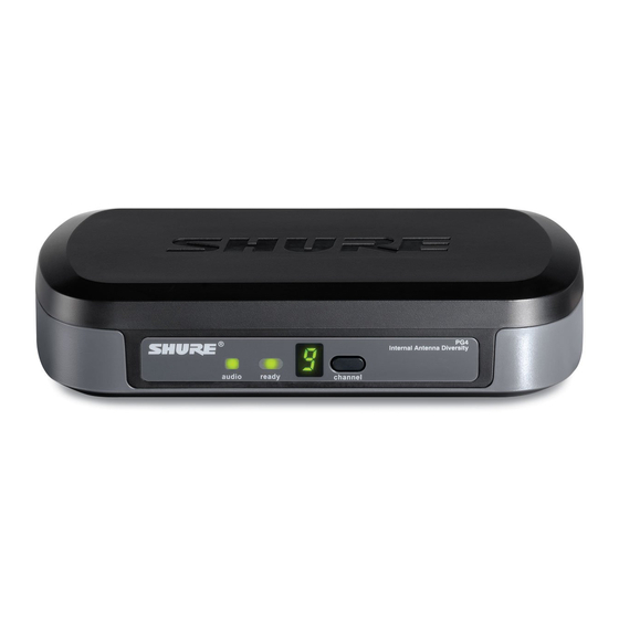
DETAILED DESCRIPTION Front Panel 1 audio LED Indicates strength of incoming audio signal: green for normal, amber for strong, red for peak. 2 ready LED Green light indicates system is ready for use. 3 LED screen 4 channel button Back Panel 1 AC adapter jack 2 Adapter cord tie-off 3 XLR balanced microphone output jack... - Page 3 IF strip, ceramic filter, detector, RSSI buffer, low pass filter, RMS detector and expander, mute circuit, balanced and unbalanced audio outputs, tonekey detection circuit, noise squelch circuit, microprocessor and several voltage regulators. The PG4 receiver has two internal antennas mounted to the circuit board via antenna connectors..
- Page 4 The first, the second VCO's and PLL The first VCO is a two-stage design composed of an oscillator stage and a buffer stage. Its frequency is controlled with the synthesizer chip IC1. The first stage (Q724) is a common emitter Colpitts oscillator. The air wound resonator L720 is coupled to the transistor with C723, and to the modulation varactor diode by C721.
- Page 5 RF & AUDIO BLOCK DIAGRAM IF/Detector From 110 MHz Buffer Buffer and 10.7 MHz MIXER SAW Filter 10.7 MHz ceramic filters DC gain Mixer Sanyo LA8662V Audio RSSI To uP output output RF – 1 and 2 LMX2335 mixer and detector LTM PLL From µP Controller Audio...
- Page 6 Digital Section The Freescale 8Kb FLASH microprocessor was chosen to maximize its benefits and to reduce system cost. The internal ADC converters are utilized to sample DC voltages to handle switching diversity, audio metering, audio muting, noise squelching, and tone-key detection. RF band detection uses four digital inputs.
- Page 7 Four resistors Ra, Rb, Rc, and Rd are responsible to start the microcontroller in a RF band. Table 2 shows the reference designators and how the voltages at the test points reflect the operating RF band. Table 2 PG4 Reference Designators R316 R315...
- Page 8 Microcontroller Netnames and Programming Testpoint List Port Name Testpoint RESETn Reset TP_RST PTC0/TxD2 Seven Segment A PTC1/RxD2 Seven Segment B PTC2/SDA1 Seven Segment C PTC3/SCL1 Seven Segment D PTC4 Seven Segment E PTC5 Seven Segment F PTC6 Seven Segment G PTC7 PTE0/TxD1 Select Button...
- Page 9 RF Level The microprocessor reads the RSSI level from an ADC several times a second when the PG4 is unmuted, to predict if a switch is neces- sary to avoid an audible dropout. Thresholds were calculated from the above RSSI curve.
- Page 10 NOTES 25A1104 (Rev.1)
- Page 11 RF Signal Generator Agilent E4420B Audio Analyzer HP 8903B Power Supply PS20 BNC (M) to BNC (M) cable (2) Shure PT1838A BNC (F) to 1/4” adapter Shure PT1838C Matching UA820 Antenna Frequency Dependent LISTENING TEST Before completely disassembling the receiver, operate it to determine whether it is functioning normally and try to duplicate the reported malfunction.
- Page 12 Deviation All other frequencies 27.5 kHz 37.5 kHz TONE KEY INDICATOR Modulate the RF signal with 32.768 kHz tone key generator. (If using an HP E4400B RF Generator use the Dual- Sine wave feature by pressing: more, FM Waveform (Sine), and Dual-Sine). Set the following: •...
- Page 13 ASSEMBLY AND DISASSEMBLY !CAUTION! Observe precautions when handling this static-sensitive device. ASSEMBLY INSTRUCTIONS (REVERSE FOR DISASSEMBLY) REF LOW BAND ANTENNA REF LOW BAND ANTENNA REF: ANTENNAS SHOWN REF: ANTENNAS SHOWN (MORE TRIANGULAR SHAPED) (MORE TRIANGULAR SHAPED) SUPERIMPOSED TO SHOW SUPERIMPOSED TO SHOW DIFFERENT POSITIONS DIFFERENT POSITIONS ANTENNA SIDE CLIPS...
- Page 14 REF HIGH BAND REF HIGH BAND LEFT LEFT REF LOW BAND REF LOW BAND LEFT LEFT REF LOW BAND, RIGHT REF LOW BAND, RIGHT REF HIGH BAND, RIGHT REF HIGH BAND, RIGHT 25A1104 (Rev.1)
- Page 15 1 GHz Frequency Counter HP 53181A Spectrum Analyzer HP 8591A Power Supply PS20 Shielded Test Lead Shure PT1838F BNC (M) to BNC (M) cable (2) Shure PT1838A BNC (F) to ¼" adapter Shure PT1838C BNC (M) to unterminated Shure PT1824...
- Page 16 ALIGNMENT AND MEASUREMENT PROCEDURE General notes The following procedures are intended for a "bench" testing environment only. The alignment procedure is sequential and does not change unless specified. Use an RG-178/U BNC male to unterminated cable for all RF connections to the antenna inputs. Keep the test cables as short as possible (less than 3 feet in length). Include the insertion loss of the cables and the connectors when performing all RF measurements.
- Page 17 POWER TEST SECTION Measure +9.0 Vdc + 0.2 /-0.2 Vdc at test point "TP_9V" Measure +5.0 Vdc + 0.1 /-0.1 Vdc at test point "TP_5V" Measure +5.0 Vdc + 0.2 /-0.2 Vdc at test point "TP_5VPLL" Measure +3.3 Vdc + 0.2 /-0.2 Vdc at test point "TP3.3V" Measure +4.5 Vdc + 0.2 /-0.2 Vdc at test point "TP_VREF"...
- Page 18 Set signal generator level= -100 dBm. Set signal generator to corresponding frequency. Measure SINAD at TPR (Pin 7 of IC610) to be equal to or greater than 12 dB. TONEKEY LEVEL DETECTION Verify the receiver is set to ATE mode Fmid frequency. Set the RF generator's amplitude to -70dBm and carrier frequency to ATE Fmid frequency.
- Page 19 NOTES 25A1104 (Rev.1)
- Page 20 AGENCY APPROVALS FCC DD4 PG4 (Part 15 "Declaration of Conformity" filed) IC RSS-123 (Canada # 616A-PG4) Professional Only CE (Declaration of Conformity to latest version of ETSI EN 301-389) ADDITIONAL PRODUCT PERFORMANCE CHARACTERISTICS (NOT TESTED IN PRODUCTION): General notes: A-weighting filter, RF testing level = -70 dBm, 33kHz Deviation @ 1 kHz modulation frequency, unless oth- erwise specified.
- Page 21 FREQUENCY TABLES Group A Group B Group C Group D Group E Group F N. & S. America N. & S. America N. & S. America Australia / France China China / Korea 536 - 548 590 - 602 662-674 674-686 P11 702-714 740-752...
-
Page 22: Product Specifications
PRODUCT SPECIFICATIONS System Working Range 75m (250 ft.) Note: actual range depends on RF signal absorption, reflection, and interference Audio Frequency Response Minimum: 45 Hz +/– 2 dB Maximum: 15 kHz (Overall system frequency depends on microphone element.) Total Harmonic Distortion 0.5%, typical Ref. -
Page 23: Troubleshooting
TROUBLESHOOTING Current draw and DC regulator tests Connect the PS20 DC power supply to CON400. Verify current draw is 120mA +/- 25mA. If the current draw is above or below above specification disconnect the 9Vdc, 5Vdc and 3.3Vdc regulated power supply feed points to each section of the receiver to deductively troubleshoot which section is causing the excessive current drain. - Page 24 under test can cause erratic and poor measurements. Verify using a spectrum analyzer that the frequency of operation under test has no interference down to -90dBm. ·Remove both CH. A & B internal antennas from CON500 & CON505. ·Set the receiver into ATE mode and to “2” (Fmid). This sets the receiver to the center operating frequency and set the am- plitude to -50dBm.
- Page 25 emitter dc measurements are not correct replace Q603. If the voltages on Q603 were correct troubleshoot for correct component placement and values back through the SAW filter FL600. Verify pin 4 of IC610 (2nd LO input) measures the respective 2nd LO frequency at approximately -12dBm. If the 2nd LO amplitude is low check the values and correct placement of all components leading back through the circuit path to the collector of Q760.
- Page 26 Fails/Weak Audio at TPBAL2/TPBAL3 1.) Confirm audio at TPE 2.) Confirm 4.5VDC at TP_Vref 3.) Confirm tone key in RF signal or R280 is shorted to disable TK 4.) Check and confirm values of C144, C150, R150, R153 5.) Check other components in vicinity Fails Tone Key at TP_TK Confirm 4.5VDC at IC232 pins 1,5, and 7.
- Page 27 NOTES 25A1104 (Rev.1)
-
Page 28: Replacement Parts
Resistors : Unless otherwise noted, all resistors are surface-mount with 1/10 W rating and 1% tolerance. Capacitors : Unless otherwise noted, non-polarized capacitors are surface-mount NPO dielectric types with a 100 V ca- pacity and a 5% tolerance, and polarized capacitors are tantalum types. PG4 MODEL VARIATION COUNTRY FREQUENCY... - Page 29 PG4 HARDWARE REPLACEMENT PART R e f e r e n c e D e s c r i p t io n S h u r e D e s ig n a t o r P a r t N u m b e r...
- Page 30 PG4 FREQUENCY DEPENDENT PARTS** F requency M 10 P 11 Q 11 R 10 R 11 R 12 T 10 C o de 2.7 pf C1 0 2.7 pf C1 1 2.7 pf 2.7 pf 2.7 pf C346 C347 2.7 pf 2.7 pf...
- Page 31 UNPLACED COMPONENT LIST** C103 C114 C165 C346 C347 C520 C521 C600 C602 C611 C612 C622 CV703 FL610 IC360 L540 L545 Q168 R168 R280 R346 R347 R360 R400 R612 R613 R776 R790 SHLD2 Y347 NOTE: APPLIES TO ALL FREQUENCY CODES 25A1104 (Rev.1)
-
Page 32: Pcb Layout
PCB LAYOUT 25A1104 (Rev.1) - Page 33 25A1104 (Rev.1)
Need help?
Do you have a question about the PG4 and is the answer not in the manual?
Questions and answers