
Subscribe to Our Youtube Channel
Related Manuals for Aaeon HSB-800I


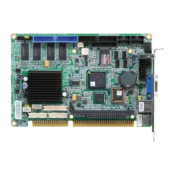
Summary of Contents for Aaeon HSB-800I
- Page 1 H a l f - s i z e S B C H S B - 8 0 0 I HSB-800I AMD LX800 Processor ISA Half-size CPU Card With DDR, Ethernet, CompactFlash™ & PC/104 HSB-800I Manual Rev. A 3rd Ed. October 2012...
-
Page 2: Copyright Notice
AAEON assumes no liabilities resulting from errors or omissions in this document, or from the use of the information contained herein. AAEON reserves the right to make changes in the product design without notice to its users. - Page 3 H a l f - s i z e C P U C a r d H S B - 8 0 0 I Acknowledgments All other products’ name or trademarks are properties of their respective owners. Award is a trademark of Award Software International, Inc. CompactFlash™...
-
Page 4: Packing List
H a l f - s i z e C P U C a r d H S B - 8 0 0 I Packing List Before you begin installing HSB-800I, please make sure that the following items have been shipped: •... -
Page 5: Table Of Contents
H a l f - s i z e C P U C a r d H S B - 8 0 0 I Contents Chapter 1 General Information 1.1 Introduction..............1-2 1.2 Feature ..............1-3 1.3 Specification .............. 1-4 Chapter 2 Quick Installation Guide 2.1 Safety Precaution ............ - Page 6 H a l f - s i z e C P U C a r d H S B - 8 0 0 I 2.17 Digital I/O (CN1) ............2-11 2.18 LPT Port Connector (LPT1) ........2-12 2.19 USB Connector (USB1~3) ........2-12 2.20 FAN Connector (CN2) ..........
- Page 7 H a l f - s i z e C P U C a r d H S B - 8 0 0 I B.3 IRQ Mapping Chart ..........B-3 B.4 DMA Channel Assignments........B-3...
-
Page 8: Chapter 1 General Information
H a l f - s i z e S B C H S B - 8 0 0 I Chapter General Information Chapter 1 General Information... -
Page 9: Introduction
H S B - 8 0 0 I 1.1 Introduction AAEON releases the economic half-size Single Board Computer (SBC) – HSB-800I, which is designed to target the industrial control and automation market. HSB-800I is based on AMD LX800 processor, which features the low power consumption and faster heat spreading to ensure the performance of the product. -
Page 10: Feature
H a l f - s i z e S B C H S B - 8 0 0 I 1.2 Features AMD LX 800 Processor Onboard 128MB DDR 400 Memory Integrated 2D/3D Graphics Accelerator, VGA Support CRT/TFT 10/100/1000Base-TX Ethernet x 1 (10/100 & GbE Optional) USB2.0 x 4/ RS-232 x 3, RS-232/422/485 x 1/ Parallel x 1/ IrDA Port x 1... -
Page 11: Specification
H a l f - s i z e S B C H S B - 8 0 0 I 1.3 Specification System Processor AMD LX800 System Memory Onboard 128MB DDR 400 Memory Chipset AMD LX800 + CS5536 Ethernet PCI 10/100Mbps or 10/100/1000Mbps LAN x 1 (optional), RJ-45 x 1, Realtek 8100C/8110S controller optional... - Page 12 H a l f - s i z e S B C H S B - 8 0 0 I Display: Supports CRT and LCD Simultaneous Display VGA Controller AMD LX800 Memory Shared memory up to 16M Resolutions 1600x1200 @ 32bpp at 100MHz for CRT;...
-
Page 13: Chapter 2 Quick Installation Guide
H a l f - s i z e S B C H S B - 8 0 0 I Chapter Quick Installation Guide Chapter 2 Quick Installation Guide... -
Page 14: Safety Precaution
H a l f - s i z e S B C H S B - 8 0 0 I 2.1 Safety Precautions Always completely disconnect the power cord from your board whenever you are working on it. Do not make connections while the power is on, because a sudden rush of power can damage sensitive electronic components. -
Page 15: Location Of Connectors And Jumpers
H a l f - s i z e S B C H S B - 8 0 0 I 2.2 Location of Connectors and Jumpers Component Side Solder Side Chapter 2 Quick Installation Guide... -
Page 16: Mechanical Drawings
H a l f - s i z e S B C H S B - 8 0 0 I 2.3 Mechanical Drawing Component Side Chapter 2 Quick Installation Guide... - Page 17 H a l f - s i z e S B C H S B - 8 0 0 I Solder Side 72.37 Chapter 2 Quick Installation Guide...
-
Page 18: List Of Jumpers
H a l f - s i z e S B C H S B - 8 0 0 I 2.4 List of Jumpers The board has a number of jumpers that allow you to configure your system to suit your application. The table below shows the function of each of the board's jumpers: Label Function... - Page 19 H a l f - s i z e S B C H S B - 8 0 0 I IrDA Connector LPT1 LPT Port Connector USB1~3 USB Connector USB4 USB Connector 10/100 or 100/1000 Base-TX Ethernet LAN1 Connector DIMM1 DDRII SODIMM Slot (Optional) Digital I/O Fan Connector...
-
Page 20: Setting Jumpers
H a l f - s i z e S B C H S B - 8 0 0 I 2.6 Setting Jumpers You configure your card to match the needs of your application by setting jumpers. A jumper is the simplest kind of electric switch. It consists of two metal pins and a small metal clip (often protected by a plastic cover) that slides over the pins to connect them. -
Page 21: Cfd Voltage 3.3V/5V Selection (Jp1)
H a l f - s i z e S B C H S B - 8 0 0 I 2.7 CFD Voltage 3.3V/5V Selection (JP1) Function 3.3V (default) 2.8 Clear CMOS (JP2) Function Normal (default) Clear CMOS 2.9 AT/ATX Power Type Selection (JP3) Function ATX Power Supply (default) Open... -
Page 22: Front Panel Connector (Fp1)
H a l f - s i z e S B C H S B - 8 0 0 I 2.12 Front Panel Connector (FP1) Signal Signal Power On Button (+) Reset Switch (+) Power On Button (-) Reset Switch (-) IDE LED (+) Power LED (+) IDE LED (-) -
Page 23: Rs-232/422/485 Serial Port Connector (Com2)
H a l f - s i z e S B C H S B - 8 0 0 I 2.15 RS-232/422/485 Serial Port Connector (COM2) Signal Signal DCD (422TXD-/485DATA-) RXD (422RXD+) TXD (422TXD+/485DATA+) DTR (422RXD-) 2.16 IrDA Connector (IR1) Signal IRRX IRTX... -
Page 24: Lpt Port Connector (Lpt1)
H a l f - s i z e S B C H S B - 8 0 0 I 2.18 LPT Port Connector (LPT1) Signal Signal #STROBE #AFD DATA0 #ERROR DATA1 #INIT DATA2 #SLIN DATA3 DATA4 DATA5 DATA6 DATA7 #ACK BUSY SELECT... -
Page 25: Fan Connector (Cn2)
H a l f - s i z e S B C H S B - 8 0 0 I 2.20 FAN Connector (CN2) Signal Speed Sense 2.21 Audio Input/ Output/ CD-in/ MIC (CN3) Signal Signal MIC_Vcc Audio Ground CD_GND LINE_IN L CD_L LINE_IN R... -
Page 26: Tft Lcd (Cn5)
H a l f - s i z e S B C H S B - 8 0 0 I 2.23 TFT LCD (CN5) For 24-bit TFT LCD Signal Signal +5VLCD +5VLCD +3.3VLCD +3.3VLCD BKL_EN LCD_CLK LCD_VS LCD_DE LCD_HS 2-14 Chapter 2 Quick Installation Guide... - Page 27 H a l f - s i z e S B C H S B - 8 0 0 I For 18-bit TFT LCD Signal Signal +5VLCD +5VLCD +3.3VLCD +3.3VLCD BKL_EN LCD_CLK LCD_VS LCD_DE LCD_HS 2-15 Chapter 2 Quick Installation Guide...
-
Page 28: 5Vsb Power Connector (Cn6)
H a l f - s i z e S B C H S B - 8 0 0 I 2.24 +5VSB Power Connector (CN6) Signal PS_ON# +5VSB 2.25 AT Power_5V, 12V Connector (CN7) Signal +12V 2.26 LVDS1, 2 (CN9, CN10) Signal Signal BKL_EN... -
Page 29: Ps2 Keyboard/ Mouse Connector (Cn11)
H a l f - s i z e S B C H S B - 8 0 0 I VLCD 2.27 PS2 Keyboard/ Mouse Connector (CN11) Signal KB_DATA MS-DATA KB_CLK MS_CLK 2.28 Internal Keyboard Connector (CN12) Signal KB_CLK KB_DATA 2-17 Chapter 2 Quick Installation Guide... - Page 30 H a l f - s i z e S B C H S B - 8 0 0 I Below Table for China RoHS Requirements 产品中有毒有害物质或元素名称及含量 AAEON Main Board/ Daughter Board/ Backplane 有毒有害物质或元素 部件名称 铅 汞 镉 六价铬 多溴联苯...
-
Page 31: Chapter 3 Award Bios Setup
H a l f - s i z e S B C H S B - 8 0 0 I Chapter Award BIOS Setup Chapter 3 Award BIOS Setup... - Page 32 3. The CMOS memory has lost power and the configuration information has been erased. The HSB-800I CMOS memory has an integral lithium battery backup for data retention. However, you will need to replace the complete unit when it finally runs down.
- Page 33 H a l f - s i z e S B C H S B - 8 0 0 I 3.2 Award BIOS Setup Awards BIOS ROM has a built-in Setup program that allows users to modify the basic system configuration. This type of information is stored in battery-backed CMOS RAM so that it retains the Setup information when the power is turned off.
- Page 34 Save CMOS value changes to CMOS and exit setup. Exit Without Saving Abandon all CMOS value changes and exit setup. For more detailed information, you can refer to the "AAEON BIOS Item Description.pdf" file in the CD for the meaning of each setting in this chapter.
-
Page 35: Chapter 4 Driver Installation
H a l f - s i z e S B C H S B - 8 0 0 I Chapter Driver Installation Chapter 4 Driver Installation... - Page 36 H a l f - s i z e S B C H S B - 8 0 0 I The HSB-800I comes with a CD-ROM that contains all drivers your need. Follow the sequence below to install the drivers: Step 1 –...
- Page 37 H a l f - s i z e S B C H S B - 8 0 0 I 4.1 Installation: Insert the HSB-800I CD-ROM into the CD-ROM Drive. And install the drivers from Step 1 to Step 5 in order. Step 1 –Install LX-Graphic Driver Place the Driver CD-ROM into your CD-ROM drive and follow the steps below to install.
- Page 38 H a l f - s i z e S B C H S B - 8 0 0 I Step 2 –Install AES Driver Place the Driver CD-ROM into your CD-ROM drive and follow the steps below to install. 1.
- Page 39 H a l f - s i z e S B C H S B - 8 0 0 I 3. Click on Control Panel button 4. Click on System button 5. Select Hardware and click on Device Manager… 6. Double click on Other PCI Bridge Device 7.
- Page 40 H a l f - s i z e S B C H S B - 8 0 0 I Step 5– Install Audio Driver Place the Driver CD-ROM into your CD-ROM drive and follow the steps below to install. 1.
-
Page 41: Appendix A Programming The Watchdog Timer
H a l f - s i z e S B C H S B - 8 0 0 I Appendix Programming the Watchdog Timer A - 1 Appendix A Programming the Watchdog Timer... -
Page 42: Programming
H a l f - s i z e S B C H S B - 8 0 0 I A.1 Programming HSB-800I utilizes ITE 8712 chipset as its watchdog timer controller. ( K version ) Below are the procedures to complete its configuration and... - Page 43 H a l f - s i z e S B C H S B - 8 0 0 I There are three steps to complete the configuration setup: (1) Enter the MB PnP Mode; (2) Modify the data of configuration registers;...
- Page 44 H a l f - s i z e S B C H S B - 8 0 0 I Configure Control (Index=02h) This register is write only. Its values are not sticky; that is to say, a hardware reset will automatically clear the bits, and does not require the software to clear them.
-
Page 45: Ite8712 Watchdog Timer Initial Program
H a l f - s i z e S B C H S B - 8 0 0 I WDT output through PWROK1/PWROK2 (pulse) enable note Select the interrupt level for WDT WatchDog Timer Time-out Value (LSB) Register (Index=73h, Default=00h) Description WDT Time-out value 7-0... - Page 46 H a l f - s i z e S B C H S B - 8 0 0 I Watch_Dog_Setting: ;Timer setting mov al, cl mov cl, 73h call Superio_Set_Reg ;Clear by keyboard or mouse interrupt mov al, 0f0h mov cl, 71h call Superio_Set_Reg ;unit is second.
- Page 47 H a l f - s i z e S B C H S B - 8 0 0 I MOV DX,02Eh MOV CX,04h Init_1: MOV AL,BYTE PTR CS:[SI] OUT DX,AL INC SI LOOP Init_1 Enter_Configuration_Mode ENDP Exit_Configuration_Mode PROC NEAR MOV AX,0202h CALL Write_Configuration_Data Exit_Configuration_Mode ENDP...
- Page 48 H a l f - s i z e S B C H S B - 8 0 0 I CMP AL,12h JNE Not_Initial Need_Initial: Not_Initial: Check_Chip ENDP Read_Configuration_Data PROC NEAR MOV DX,WORD PTR CS:[Cfg_Port+04h] OUT DX,AL MOV DX,WORD PTR CS:[Cfg_Port+06h] IN AL,DX Read_Configuration_Data ENDP Write_Configuration_Data PROC NEAR...
- Page 49 H a l f - s i z e S B C H S B - 8 0 0 I Write_Configuration_Data ENDP Superio_Set_Reg proc near push ax MOV DX,WORD PTR CS:[Cfg_Port+04h] mov al,cl out dx,al pop ax inc dx out dx,al Superio_Set_Reg endp.Set_Logic_Device proc near Set_Logic_Device proc near push ax...
- Page 50 H a l f - s i z e S B C H S B - 8 0 0 I Cfg_Port DB 087h,001h,055h,055h DW 02Eh,02Fh END Main Note: Interrupt level mapping 0Fh-Dh: not valid 0Ch: IRQ12 03h: IRQ3 02h: not valid 01h: IRQ1 00h: no interrupt selected A - 10...
-
Page 51: Appendix B I/O Information
H a l f - s i z e S B C H S B - 8 0 0 I Appendix I/O Information Appendix B I/O Information B-1... -
Page 52: I/O Address Map
H a l f - s i z e S B C H S B - 8 0 0 I B.1 I/O Address Map Appendix B I/O Information B-2... -
Page 53: Memory Address Map
H a l f - s i z e S B C H S B - 8 0 0 I B.2 Memory Address Map B.3 IRQ Mapping Chart B.4 DMA Channel Assignments Appendix B I/O Information B-3...
Need help?
Do you have a question about the HSB-800I and is the answer not in the manual?
Questions and answers