Table of Contents
Advertisement
Quick Links
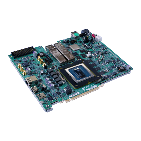
VPK120 Evaluation Board
User Guide
UG1568 (v1.0) August 9, 2022
Xilinx is creating an environment where employees, customers, and
partners feel welcome and included. To that end, we're removing non-
inclusive language from our products and related collateral. We've
launched an internal initiative to remove language that could exclude
people or reinforce historical biases, including terms embedded in our
software and IPs. You may still find examples of non-inclusive
language in our older products as we work to make these changes and
align with evolving industry standards. Follow this
link
for more
information.
Advertisement
Table of Contents

Related Manuals for AMD XILINX VPK120


Summary of Contents for AMD XILINX VPK120
- Page 1 VPK120 Evaluation Board User Guide UG1568 (v1.0) August 9, 2022 Xilinx is creating an environment where employees, customers, and partners feel welcome and included. To that end, we’re removing non- inclusive language from our products and related collateral. We’ve launched an internal initiative to remove language that could exclude people or reinforce historical biases, including terms embedded in our software and IPs.
-
Page 2: Table Of Contents
Table of Contents Chapter 1: Introduction ....................4 Overview............................4 Navigating Content by Design Process..................5 Additional Resources........................6 Block Diagram..........................6 Board Features..........................7 Board Specifications........................9 Chapter 2: Board Setup and Configuration ............11 Standard ESD Measures......................11 Board Component Location.....................11 Default Jumper and Switch Settings..................16 Versal ACAP Configuration.......................19 Chapter 3: Board Component Descriptions ........... - Page 3 Revision History......................... 63 Please Read: Important Legal Notices................... 63 UG1568 (v1.0) August 9, 2022 www.xilinx.com Send Feedback VPK120 Board User Guide...
-
Page 4: Chapter 1: Introduction
Chapter 1: Introduction Chapter 1 Introduction Overview The VPK120 evaluation board features the Xilinx ® Versal ® ACAP XCVP1202 device. The VPK120 board enables the demonstration, evaluation, and development of the applications listed here, as well as other customer applications. Many features found on the VPK120 board are subsets of existing Versal ACAP boards (e.g., the VCK190 and VMK180 boards). -
Page 5: Navigating Content By Design Process
Chapter 1: Introduction Table 1: Models of VPK120 Evaluation Boards Description EK-VPK120-G Xilinx Versal ACAP VPK120 evaluation kit EK-VPK120-G-J Xilinx Versal ACAP VPK120 evaluation kit, Japan specific EK-VPK120-G-ED (encryption Xilinx Versal ACAP VPK120 evaluation kit, China and Russia specific disabled) Users of encryption-disabled kits will not be able to access the following features: •... -
Page 6: Additional Resources
Chapter 1: Introduction • Board System Design: Designing a PCB through schematics and board layout. Also involves power, thermal, and signal integrity considerations. For more information, see Versal ACAP Design Process Documentation Board System Design. Additional Resources Appendix D: Additional Resources and Legal Notices for references to documents, files, and resources relevant to the VPK120 evaluation board. -
Page 7: Board Features
Chapter 1: Introduction Board Features The VPK120 evaluation board features are listed here. Detailed information for each feature is provided in Chapter 3: Board Component Descriptions. • XCVP1202, VSVA2785 package • Form factor: extended height PCIe , double-slot (heatsink clearance) ®... - Page 8 Chapter 1: Introduction PL GPIO DIP switch (4-position) ○ PL GPIO LEDs (four) ○ PL GPIO pushbuttons (two) ○ PL trace connector (J332) ○ PL SYSCTLR_GPIO[0:15] ○ PL 8A34001_GPIO[0:15] ○ • 28 GTYP transceivers (7 quads) PCIe 16-lane edge connector (16, banks GTYP102 - GTYP105) ○...
-
Page 9: Board Specifications
Chapter 1: Introduction PS LPD MIO [21:22]: optional fan interface ○ LPD MIO[23]: VADJ_FMC power rail ○ • Security: PSBATT button battery backup • SYSMON header • Operational switches (power on/off, PROG_B, boot mode DIP switch) • Operational status LEDs (INIT, DONE, PS STATUS, PGOOD) Power and Status LEDs ○... - Page 10 Chapter 1: Introduction Storage: –25°C to +60°C • Humidity: 5% to 95% non-condensing Operating Voltage +12 V Mechanical The VPK120 evaluation board includes a mechanical stiffener to help ensure success with the board under normal lab conditions and use. While it is recommended to not remove this stiffener, it is understood that it might be necessary to remove it for continued evaluation.
-
Page 11: Chapter 2: Board Setup And Configuration
Chapter 2: Board Setup and Configuration Chapter 2 Board Setup and Configuration Standard ESD Measures CAUTION! ESD can damage electronic components when they are improperly handled, and can result in total or intermittent failures. Always follow ESD-prevention procedures when removing and replacing components. - Page 12 Chapter 2: Board Setup and Configuration IMPORTANT! The following figure is for visual reference only and might not reflect the current revision of the board. IMPORTANT! There could be multiple revisions of this board. The specific details concerning the differences between revisions are not captured in this document. This document is not intended to be a reference design guide and the information herein should not be used as such.
- Page 13 Chapter 2: Board Setup and Configuration CAUTION! Do NOT plug a PC ATX power supply 6-pin connector into the VPK120 board power connector J16. The ATX 6-pin connector has a different pinout than J16. Connecting an ATX 6-pin connector into J16 damages the VPK120 board and voids the board warranty. Table 2: Board Component Locations Callout Schematic...
- Page 14 Chapter 2: Board Setup and Configuration Table 2: Board Component Locations (cont'd) Callout Schematic Ref. Des. Feature Notes Page U160 VCC_PMC/PSFP/VCCO_MIO/ Infineon IRPS5401MTRPBF VCCAUX/VCC1V5 regulator IC PMU 5-Ch step-down DC/DC U167 VCCAUX_PMC/LPDMGTYAVCC/ Infineon IRPS5401MTRPBF MGTVCCAUX/MGTAVCC IC PMU 5-Ch step-down DC/DC regulator U175 VCCO_502/UTIL_2V5/...
- Page 15 Chapter 2: Board Setup and Configuration Table 2: Board Component Locations (cont'd) Callout Schematic Ref. Des. Feature Notes Page U248 LPDDR4 CLK1, 200 MHz, 3.3V Skyworks/Silicon Labs 570BAB000299DGR LVDS, 0x60 Osc. XO 10-810 MHz Bottom of board LPDDR4 CLK2, 200 MHz, 3.3V Skyworks/Silicon Labs 570BAB000299DGR LVDS, 0x60 Osc.
-
Page 16: Default Jumper And Switch Settings
Chapter 2: Board Setup and Configuration Default Jumper and Switch Settings The following figure shows the VPK120 board jumper header and switch locations. Each numbered component shown in the figure is keyed to the applicable table in this section. Both tables reference the respective schematic page numbers. - Page 17 Chapter 2: Board Setup and Configuration Table 3: Default Jumper Settings Callout Schematic Ref. Des. Function Default Number Page SYSMON VREFP SEL 1-2: External VREF 2-3: Disable external VREF POR_B supervisor SENSE input 1-2: VCCO_MIO ramp-up sense (1.8V) 2-3: VCCAUX_PMC ramp-up sense (1.5V) J326 POR_B enable header 1-2, 3-4 jumpered...
- Page 18 Chapter 2: Board Setup and Configuration Switches The following table lists the default switch settings. Table 4: Default Switch Settings Callout Schematic Ref. Des. Function Default Number Page U1 mode 4-Pole DIP switch ON, OFF, OFF, OFF Switch OFF = 1 = high; ON = 0 = low Mode = SW1[1:4] = Mode[0:3] SD = ON,OFF,OFF,OFF = 0111 QSPI32 = ON,OFF,ON,ON = 0100...
-
Page 19: Versal Acap Configuration
Chapter 2: Board Setup and Configuration Versal ACAP Configuration The Versal XCVP1202 ACAP boot process is described in the “Platform Boot, Control, and Status” section of the Versal ACAP Technical Reference Manual (AM011). The VPK120 board supports a subset of the modes documented in the technical reference manual via onboard boot options. - Page 20 Chapter 2: Board Setup and Configuration 2-pole DIP SW3[1:2] setting is XX as the MUX is inhibited/turned off. ○ In this mode, the FT4232 device (U20) UART functionality continues to be available. ○ Power-cycle the VPK120 board or press the power-on reset pushbutton (SW2). SW2 is ○...
-
Page 21: Chapter 3: Board Component Descriptions
Chapter 3: Board Component Descriptions Chapter 3 Board Component Descriptions Overview This chapter provides a detailed functional description of the board’s components and features. The "Board Component Locations" table in Board Component Descriptions identifies the components and references the respective schematic page numbers. Component locations are shown in the "Evaluation Board Component Locations"... - Page 22 Chapter 3: Board Component Descriptions Figure 5: Encryption Key Backup Circuit X26015-080522 The Seiko TS621E rechargeable 1.5V lithium button-type battery B1 is soldered to the board with the positive output connected to the XCVP1202 ACAP U1 VCC_BATT bank pin AG33. The battery supply current IBATT specification is 150 nA maximum when board power is off.
- Page 23 Chapter 3: Board Component Descriptions Table 6: I/O Voltage Rails (cont'd) Power Supply ACAP (U1) Bank Voltage Description Rail Net Name XPIO Bank 706 VCC1V1_LP4 1.1V LPDDR4 TRIP3 CH1 XPIO Bank 707 VCC1V1_LP4 1.1V LPDDR4 TRIP3 CH0, LPDDR4 TRIP3 CH1 XPIO Bank 708 VCC1V1_LP4 1.1V...
- Page 24 Chapter 3: Board Component Descriptions Figure 6: LPDDR4 Component Memory XPIO XPIO XPIO Triplet 1 Triplet 2 Triplet 3 LPDDR4 LPDDR4 LPDDR4 2x (1x32) 2x (1x32) 2x (1x32) X26003-080522 XCVP1202 U1 has been configured with three triplet banks. • XPIO triplet 1 (banks 700/701/702) •...
- Page 25 Chapter 3: Board Component Descriptions POR_B is the Versal ACAP processor reset, which can be controlled by: • SYSCTLR (U125) • PC4 header (J36) • FTDI USB JTAG chip (U20) In the following figure, U235 allows directional open drain level shifting for all of these masters, and J326 allows them to be bused together if desired.
- Page 26 Chapter 3: Board Component Descriptions Figure 7: POR_B Reset Circuit X26016-111821 UG1568 (v1.0) August 9, 2022 www.xilinx.com Send Feedback VPK120 Board User Guide...
- Page 27 Chapter 3: Board Component Descriptions PMC and LPD MIO The following sections provide the MIO peripheral mapping implemented on the VPK120 evaluation board. See the Versal ACAP Technical Reference Manual (AM011) for more information on MIO peripheral mapping. Additional signal connectivity can be located in the following schematic sections: •...
- Page 28 Chapter 3: Board Component Descriptions Table 7: MIO Peripheral Mapping (cont'd) PMC MIO[0:25] Bank 500 PMC MIO[26:51] Bank 501 LPD MIO[0:25] Bank 502 USB3320 U99 GEM0 PMC MIO[0–12] Bank 500: QSPI U11, U12 [Figure 3, callout 37] The VPK120 evaluation board uses two Micron MT25QU01GBBB8E12-0SIT 4-bit serial peripheral interface (quad SPI) flash devices.
- Page 29 Chapter 3: Board Component Descriptions Figure 8: Dual Parallel QSPI Circuit X26295-021422 PMC MIO[13:25] Bank 500: USB 2.0 ULPI PHY The VPK120 evaluation board uses a Standard Microsystems Corporation USB3320 USB 2.0 ULPI transceiver (U99) to support a USB 2.0 type-A connector (J308). The USB3320 is a high- speed USB 2.0 PHY supporting the UTMI+ low pin interface (ULPI) interface standard.
- Page 30 Chapter 3: Board Component Descriptions The USB3320 ULPI transceiver circuit has a Micrel MIC2544 high-side programmable current limit switch (U100). This switch has an open-drain output fault flag on pin 2, which turns on red LED DS37 if over current or thermal shutdown conditions are detected. Note: As shown in the following figure, the shield for the USB 2.0 type-A connector (J308) can be tied to GND by a jumper on header J300 pins 1-2 (see Default Jumper and Switch...
- Page 31 Chapter 3: Board Component Descriptions The VPK120 evaluation board includes a secure digital input/output (SDIO) interface to provide access to general purpose non-volatile SDIO memory cards and peripherals. This interface is used for the SD boot mode and supports SD2.0 and SD3.0 access. The SDIO interface signals PMC_MIO[26:36, 51] are connected to XCVP1202 ACAP bank 501, which has its VCCO set to 1.8V.
- Page 32 Chapter 3: Board Component Descriptions Table 8: NVT4857UK U104 Adapter Pinout (cont'd) Aries Adapter Pin Number NVT4857UKAZ Pin Number NVT4857UKAZ Pin Name Unused Unused DATA0 DAT3A DAT1A Unused Unused DAT2A DAT1B DAT0B CLKB CMDB DAT3B DAT2B Unused Unused The ACAP (U1) also has control over the power for the SDCARD, which allows the ACAP to remove power to the SD card as needed.
- Page 33 Chapter 3: Board Component Descriptions Information for the SD I/O card specification can be found at the SanDisk Corporation Association websites. The VPK120 SD card interface supports the SD1 (2.0) and SD2 (3.0) configuration boot modes documented in the Versal ACAP Technical Reference Manual (AM011). See schematic page 39 for more details.
- Page 34 Chapter 3: Board Component Descriptions Figure 12: FT4232HL UART Connections FMC+ FTDI XCVC1202 ACAP Versal JTAG TDI/TDO PortA USB2.0 Versal PS UART PortB PS UART Versal PL UART PortC PL UART HSDP SysCon UART PortD J344 ZX62D-AB-5P8 MPSoC JTAG PS UART X26062-030322 For more information on the FT4232HL, see the Future Technology Devices International Ltd.
- Page 35 Chapter 3: Board Component Descriptions Figure 13: I2C1 Bus Topology I2C1 0x74 0x74 REF_CLK_I2C System Controller FMCP1_IIC U213 PS Bank 501 LPDDR4_SI570_CLK3 U125 XCZU4EG LPDDR4_SI570_CLK2 Versal ACAP LPDDR4_SI570_CLK1 U211 QSFPDD_I2C PS Bank 501 8A34001 U35 TCA9548A U35 TCA9548A 0x54 & 0x5C EEPROM U34 M24128 I2C1...
- Page 36 Chapter 3: Board Component Descriptions Bus I2C0 connects the XCVP1202 U1 PS bank 501 and the XCZU4EG system controller U125 PS bank 501 to a GPIO 16-bit port expander (TCA6416A U233) and I2C switch (TCA9548A U33). The port expander enables accepting various fan controller, FMCP connector, and power system status inputs.
- Page 37 Chapter 3: Board Component Descriptions Table 11: I2C0 Port Expander TCA6416A U233 Address 0x20 Connections I2C Devices Port Direction Device P00-P01 QSFPDD1_MODSELL J1 QSFP-DD QSFPDD2_MODSELL J2 QSFP-DD PMBUS2_INA226_ALERT U125 (ZU4), U166, U168, U172, U174, U176, U177, U184, U186, U188, U234, U260, U264, U265 P07-P09 FMCP1_FMC_PRSNT_M2C_B J51 FMCP HSPC...
- Page 38 Chapter 3: Board Component Descriptions Figure 15: RGMII Ethernet GEM0 U198 RGMII DP83867 J307 10/100/1000 MDIO RJ45 25 MHz Crystal XCVC1202 ACAP X26023-031022 Ethernet PHY (Three Resets) [Figure 3, callout 16] The DP83867 PHY (GEM0 U198) is reset by its GEM0_RESET_B generated by dedicated pushbutton switch (SW15) and PMC_MIO signals as shown in the following figure.
- Page 39 Chapter 3: Board Component Descriptions Ethernet PHY LED Interface [Figure 3, callout 16] Each DP83867 PHY (GEM0 U198) controls two LEDs in the J307 two port connector bezel. The PHY signal LED0 drives the green LED, and LED1 drives the yellow LED. The LED2 signal is not used.
- Page 40 Chapter 3: Board Component Descriptions Table 14: PMC MIO[49] and LPD MIO[13,15:16,20] Power Domains ACAP Pin Signal Power Domains PMC MIO49 VCC_PSLP_EN LPDMGTYAVCC, VCCO_502, VCC_PSLP_CPM5, LPDMGTYAVTT LPD MIO 13 VCC_SOC_EN VCC_SOC LPD MIO 15 VCC_PSFP_EN VCC_PSFP LPD MIO 16 VCC1V1_LP4_AUX_EN VCCAUX,VCC1V1_LP4 LPD MIO 20 VCC_PL_EN...
- Page 41 Chapter 3: Board Component Descriptions • If no valid information is found in an attached FMC card IIC EEPROM, the VADJ_FMC rail is set to 0.0V The system controller user interface allows the FMC IPMI routine to be overridden and an explicit value can be set for the VADJ_FMC rail.
- Page 42 Chapter 3: Board Component Descriptions Figure 17: JTAG Chain Block Diagram U125 XCZU4EG BANK 44 SYSTEM CONTROLLER UTIL_3V3 4.70K 4.70K Set to “ON OFF” for FTDI JTAG FMC1 R162 SYSCTLR JTAG 4.70K FT4232 JTAG UTIL 3v3 NOTE: Switch open when FMC present. B-to-A ACAP U1 S1 S0 OEn...
- Page 43 Chapter 3: Board Component Descriptions Table 15: Clock Sources Schematic Ref. Des. Feature Notes Page U248 DDR4 DIMM CLK, 200 MHz, 3.3V LVDS, 0x60 Skyworks/Silicon Labs 570BAB000299DG DDR4 DIMM CLK, 200 MHz, 3.3V LVDS, 0x60 Skyworks/Silicon Labs 570BAB000299DG DDR4 DIMM CLK, 200 MHz, 3.3V LVDS, 0x60 Skyworks/Silicon Labs 570BAB000299DG ACAP U1 REF CLK, 33.33 MHz, 1.8V CMOS, 0x5D...
- Page 44 Chapter 3: Board Component Descriptions The VPK120 evaluation board has an I2C programmable SI570 low-jitter 1.8V CMOS single- ended oscillator (U32). The 33.333 MHz REF_CLK clock signal is connected to XCVP1202 ACAP U1 configuration bank 503. At power-up, this clock defaults to an output frequency of 33.333333...
- Page 45 Chapter 3: Board Component Descriptions The 8A34001 synchronization management unit (SMU) provides tools to manage timing references, clock sources, and timing paths for IEEE 1588 and Synchronous Ethernet (SyncE) based clocks. The PLL channels can act independently as frequency synthesizers, jitter attenuators, digitally controlled oscillators (DCO), or digital phase lock loops (DPLL).
- Page 46 Chapter 3: Board Component Descriptions Table 16: Transceiver Mapping VPK120 XCVP1202 VSVA2785 GTY/GTM Mapping [Unused] GTM SMA [Unused] 8A34001 1PPS Clocks GTYP MRMAC [Unused] [Unused] Quad 106 PCIe X0Y1 Quad 206 X0Y1 X0Y6 X0Y4 [Unused] [Unused] [Unused] refclk1 refclk1 8A34001 CLK6 IN [Unused] refclk0 refclk0...
- Page 47 Chapter 3: Board Component Descriptions Table 16: Transceiver Mapping (cont'd) VPK120 XCVP1202 VSVA2785 GTY/GTM Mapping FMC DP7 FMC DP6 GTYP FMC DP5 MRMAC Quad 201 X0Y0 FMC DP4 X1Y1 refclk1 SI570_BUF1 refclk0 FMCP1_GBTCLK1 FMC DP3 FMC DP2 GTYP FMC DP1 PCIe Quad 200 X1Y0...
- Page 48 Chapter 3: Board Component Descriptions GTYP200/201: FPGA Mezzanine Card Interface [Figure 3, callout 17] The detailed ACAP connections for the feature described in this section are documented in the VPK120 board XDC file, referenced in Appendix B: Xilinx Design Constraints. FMC+ Connector Type The Samtec SEAF series 1.27 mm (0.050 in) pitch mates with the SEAM series connector.
- Page 49 Chapter 3: Board Component Descriptions Note: QSFP-DD1, J1, supports legacy QSFP operation up to 112G using four odd channels only while full eight channels QSFP-DD operation supports up to 56 Gb/s. QSFP-DD2, J2, supports legacy QSFP 4 channel and QSFP-DD eight channel support up to 56 Gb/s (no 112 Gb/s support). See the Versal ACAP GTM Transceivers Architecture Manual (AM017) for more details on 112 Gb/s GTM-Quad limitations.
- Page 50 Chapter 3: Board Component Descriptions Table 18: User I/O (cont'd) Net Name Ref. Designator Schematic Pages GPIO_PB1 7/48 GPIO_DIP_SW0 7/48 GPIO_DIP_SW1 7/48 GPIO_DIP_SW2 7/48 GPIO_DIP_SW3 7/48 GPIO_LED_0_LS 7/48 GPIO_LED_1_LS 7/48 GPIO_LED_2_LS 7/48 GPIO_LED_3_LS 7/48 Power and Status LEDs [Figure 3, callout 31] The following figure shows the power and status LEDs.
- Page 51 Chapter 3: Board Component Descriptions Figure 19: Power and Status LEDs Schematic Ref. Voltage Name VCCAUX_PMC_PG DS15 VCCAUX_PG DS16 VCC_PSFP_PG DS13 VCC_PSLP_CPMS_PG DS14 VCC_RAM_VCCINT_GT_PG DS12 VCC_PMC_PG DS11 VCC_SOC_PG DS10 VCCINT_PG UTIL_3V3_PG DS32 UTIL_2V5_PG DS43 UTIL_1VS3_PG DS29 MGTYVCCAUX_PG DS30 MGTYAVTT_PT DS27 MGTYVCC_PG DS28 VADI_FMC_PG...
- Page 52 Chapter 3: Board Component Descriptions The VPK120 board provides a fan controller bypass header J347 and J348 to permit control by the Versal ACAP. See the Default Jumper and Switch Settings for more details. Figure 20: 12V Fan Header X26028-121021 System Controller [Figure 3, callout 50]...
- Page 53 Chapter 3: Board Component Descriptions 5. Launch the board user interface application. The board user interface application UI is shown in the following figure. Figure 21: System Controller User Interface X26030-112221 The system controller user interface (SCUI) buttons gray out during command execution and return to their original appearance when ready to accept a new command.
- Page 54 Chapter 3: Board Component Descriptions The VPK120 board power switch is SW13. Sliding the switch actuator from the off to the on position applies 12VDC power from either the 2x3 6-pin mini-fit power input connector J16 (power from an external 120VAC-to-12VDC power adapter) or the 2x4 8-pin ATX power supply PCIe-type connector JP1.
- Page 55 Chapter 3: Board Component Descriptions Table 19: Power System - PMBus Regulators and INA226 Map Regulator Ref. Vout Iout PMBUS INA226 Ref. INA226 I2C Rail Name Type Des. Addr. Addr. Des. Addr. VCC_INT IR35215 PMIC U152 0.80 0x40 BUS1 0x46 0x16 VCC_SOC 0.80...
- Page 56 Chapter 3: Board Component Descriptions Table 20: Power System – Non-PMBus Regulators (cont'd) Rail Name Regulator Type Ref. Des. Vout (V) Iout (A) SYS_VCC1V2 TPS62097RWKR U147 SYS_VCC1V1 TPS7A8300ARGR U145 8A34001_VCC_GPIO_DC LP38798SD-ADJ/NOPB U223 8A34001_VDDA LP38798SD-ADJ/NOPB U225 8A34001_VDDO_Q1_10_7 LP38798SD-ADJ/NOPB U226 8A34001_VDD_CLK0 LP38798SD-ADJ/NOPB U227 8A34001_VDDO_Q0_9_6 LP38798SD-ADJ/NOPB...
-
Page 57: Appendix A: Vita 57.4 Fmcp Connector Pinouts
Appendix A: VITA 57.4 FMCP Connector Pinouts Appendix A VITA 57.4 FMCP Connector Pinouts Overview The following figure shows the pinout of the FPGA plus mezzanine card (FMCP) high pin count (HSPC) connector defined by the VITA 57.4 FMC specification. For a description of how the VPK120 evaluation board implements the FMCP specification, see GTYP200/201: FPGA Mezzanine Card... -
Page 58: Appendix B: Xilinx Design Constraints
Appendix B: Xilinx Design Constraints Appendix B Xilinx Design Constraints Overview The Xilinx ® design constraints (XDC) file template for the VPK120 board provides for designs targeting the VPK120 evaluation board. Net names in the constraints listed correlate with net names on the latest VPK120 evaluation board schematic. -
Page 59: Appendix C: Regulatory And Compliance Information
Appendix C: Regulatory and Compliance Information Appendix C Regulatory and Compliance Information This product is designed and tested to conform to the European Union directives and standards described in this section. For Technical Support, open a Support Service Request. CE Information CE Directives 2006/95/EC, Low Voltage Directive (LVD) 2004/108/EC, Electromagnetic Compatibility (EMC) Directive... -
Page 60: Compliance Markings
Appendix C: Regulatory and Compliance Information Compliance Markings In August of 2005, the European Union (EU) implemented the EU Waste Electrical and Electronic Equipment (WEEE) Directive 2002/96/EC and later the WEEE Recast Directive 2012/19/EU. These directives require Producers of electronic and electrical equipment (EEE) to manage and finance the collection, reuse, recycling and to appropriately treat WEEE that the Producer places on the EU market after August 13, 2005. -
Page 61: Appendix D: Additional Resources And Legal Notices
Appendix D: Additional Resources and Legal Notices Appendix D Additional Resources and Legal Notices Xilinx Resources For support resources such as Answers, Documentation, Downloads, and Forums, see Xilinx Support. Documentation Navigator and Design Hubs Xilinx ® Documentation Navigator (DocNav) provides access to Xilinx documents, videos, and support resources, which you can filter and search to find information. -
Page 62: References
Appendix D: Additional Resources and Legal Notices References The most up to date information related to the VPK120 board and its documentation is available on these websites: VPK120 Evaluation Kit VPK120 Evaluation Kit — Master Answer Record 00003361 These documents provide supplemental material useful with this guide: 1. - Page 63 Appendix D: Additional Resources and Legal Notices Samtec, Inc. (SEAF series connectors, LPAF connectors) VITA FMC Marketing Alliance (FPGA Mezzanine Card (FMC) VITA 57.1, 57.4 specifications) Maxim Integrated Circuits (MAX6643) Infineon Integrated Circuits (IR35215, IRPS5401, IR38164, IR3897) Future Technology Devices International Ltd. (FT4232HL) Integrated Device Technology, Inc.
- Page 64 Appendix D: Additional Resources and Legal Notices www.xilinx.com/legal.htm#tos; IP cores may be subject to warranty and support terms contained in a license issued to you by Xilinx. Xilinx products are not designed or intended to be fail-safe or for use in any application requiring fail-safe performance; you assume sole risk and liability for use of Xilinx products in such critical applications, please refer to Xilinx's Terms of Sale which can be viewed at https:/...