Table of Contents
Advertisement
Quick Links
www.ti.com
User's Guide
LM5157EVM-BST Evaluation Module
The LM5157EVM-BST evaluation module showcases the features and performance of the LM5157 device
as wide input voltage, non-synchronous boost converter with dual random spread spectrum. The standard
configuration is designed to provide a regulated output of 12 V at 1.6 A from an input of 3 V to 9 V (load derated
for input voltages below 6 V), switching at a frequency of 2.1 MHz.
1 Features and Electrical Performance...................................................................................................................................
2 Application Schematic...........................................................................................................................................................
Picture.............................................................................................................................................................................6
Procedure......................................................................................................................................................7
Results.............................................................................................................................................................................8
Files...........................................................................................................................................................................14
7 Revision History...................................................................................................................................................................
Circuit......................................................................................................................................................5
Figure 3-1. EVM Picture..............................................................................................................................................................
Figure 4-1. Test Setup.................................................................................................................................................................
Load......................................................................................................................................................8
Figure 5-2. Load Regulation........................................................................................................................................................
Figure 5-4. Thermal Image V
= 3 V, I
IN
IN
IN
Figure 6-1. Top Layer and Silkscreen........................................................................................................................................
Layer.................................................................................................................................................................14
Figure 6-3. Signal Layer 1.........................................................................................................................................................
Figure 6-4. Signal Layer 2.........................................................................................................................................................
Figure 6-5. Bottom Layer...........................................................................................................................................................
Table 1-2. Jumper Description.....................................................................................................................................................
Table 4-1. Standard Configuration Jumper Connections.............................................................................................................
SNVU739A - OCTOBER 2020 - REVISED AUGUST 2021
Submit Document Feedback
Table of Contents
List of Figures
= 3 V I
= 0.6 A, V
IN
OUT
= 0.6 A, V
= 3 V, I
= 0.6 A......................................................................................................................
IN
OUT
= 1.6 A......................................................................................................................
IN
= 1.6 A......................................................................................................................
IN
= 0.6 A (20
Ω).................................................................................................................11
OUT
= 1.6 A (7.5 Ω)................................................................................................................
Ω)................................................................................................................11
= 0.3 A to 0.6
= 0.8 A to 1.6
= 0.8 A to 1.6
= 0.6 A...................................................................................................
= 6 V, I
= 1.6A....................................................................................................
IN
OUT
= 1.6 A...................................................................................................
(mirrored)..................................................................................................................14
Schematic..................................................................................................................................15
List of Tables
Configuration..........................................................................................................3
Copyright © 2021 Texas Instruments Incorporated
ABSTRACT
= V
, no Forced Air Cooling..............................................................
= 12 V, no Forced Air Cooling............................................................
, no Forced Air Cooling..............................................................
, no Forced Air Cooling..............................................................
A....................................................................................................12
A....................................................................................................12
A....................................................................................................12
Table of Contents
LM5157EVM-BST Evaluation Module
3
5
18
6
7
8
9
9
9
9
10
10
10
11
13
13
13
14
14
14
14
4
7
1
Advertisement
Table of Contents

Related Manuals for Texas Instruments LM5157EVM-BST


Summary of Contents for Texas Instruments LM5157EVM-BST
-
Page 1: Table Of Contents
LM5157EVM-BST Evaluation Module ABSTRACT The LM5157EVM-BST evaluation module showcases the features and performance of the LM5157 device as wide input voltage, non-synchronous boost converter with dual random spread spectrum. The standard configuration is designed to provide a regulated output of 12 V at 1.6 A from an input of 3 V to 9 V (load derated for input voltages below 6 V), switching at a frequency of 2.1 MHz. - Page 2 Trademarks www.ti.com Table 6-1. LM5157EVM-BST Bill of Materials..........................16 Trademarks All trademarks are the property of their respective owners. LM5157EVM-BST Evaluation Module SNVU739A – OCTOBER 2020 – REVISED AUGUST 2021 Submit Document Feedback Copyright © 2021 Texas Instruments Incorporated...
-
Page 3: Features And Electrical Performance
Features and Electrical Performance 1 Features and Electrical Performance The LM5157EVM-BST supports the following features and performance capabilities: • Tightly regulated output voltage of 12 V with 1% accurate reference voltage • High conversion efficiency of > 92% at full load •... -
Page 4: Table 1-2. Jumper Description
Pin 5 to pin 6 (HN) Hiccup mode enabled, spread spectrum disabled J11) Pin 7 to pin 8 (NS) Hiccup mode disabled, spread spectrum enabled LM5157EVM-BST Evaluation Module SNVU739A – OCTOBER 2020 – REVISED AUGUST 2021 Submit Document Feedback Copyright © 2021 Texas Instruments Incorporated... -
Page 5: Application Schematic
Application Schematic 2 Application Schematic The LM5157EVM-BST is capable of multiple configurations. Figure 2-1 shows the standard configuration of the LM5157EVM-BST for which the parameters in Table 1-1 are valid. Section 4.2 describes the correct jumper settings and measurement locations to recreate the data presented in... -
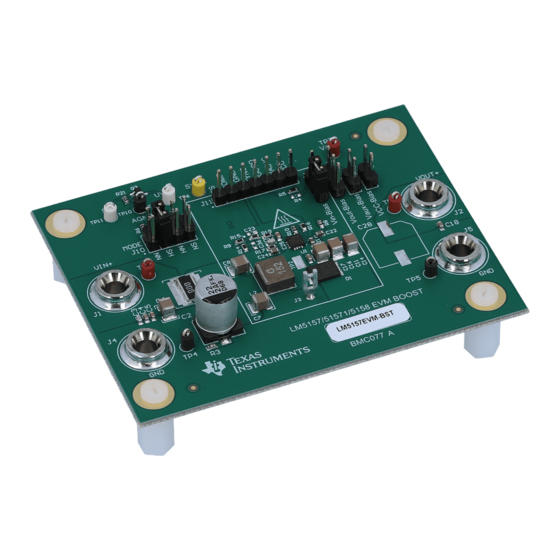
Page 6: Evm Picture
EVM Picture www.ti.com 3 EVM Picture Figure 3-1 shows the 3D-rendered picture of the LM5157EVM-BST. The actual board color can differ. Figure 3-1. EVM Picture LM5157EVM-BST Evaluation Module SNVU739A – OCTOBER 2020 – REVISED AUGUST 2021 Submit Document Feedback Copyright © 2021 Texas Instruments Incorporated... -
Page 7: Test Setup And Procedure
It is not recommended to use a long-leaded ground connection due to the possibility of noise being coupled into the signal. To measure other waveforms, adjust the oscilloscope as needed. SNVU739A – OCTOBER 2020 – REVISED AUGUST 2021 LM5157EVM-BST Evaluation Module Submit Document Feedback Copyright © 2021 Texas Instruments Incorporated... -
Page 8: Test Results
5 Test Results Figure 5-1 through Figure 5-17 present the typical performance of the LM5157EVM-BST according to the BOM and the configuration described in Section 4. Based on measurement techniques and environmental variables, measurements can differ slightly than the data presented. -
Page 9: Figure 5-3. Thermal Image
Figure 5-6. Thermal Image V = 9 V I = 1.6 A, , no Forced Air Cooling , no Forced Air Cooling BIAS BIAS SNVU739A – OCTOBER 2020 – REVISED AUGUST 2021 LM5157EVM-BST Evaluation Module Submit Document Feedback Copyright © 2021 Texas Instruments Incorporated... -
Page 10: Figure 5-7. Steady State, V
Figure 5-8. Steady State, V = 6 V, I = 1.6 A Figure 5-9. Steady State, V = 9 V, I = 1.6 A LM5157EVM-BST Evaluation Module SNVU739A – OCTOBER 2020 – REVISED AUGUST 2021 Submit Document Feedback Copyright © 2021 Texas Instruments Incorporated... -
Page 11: Figure 5-10. Start-Up, V
= 6 V, I = 1.6 A (7.5 Ω) Figure 5-12. Start-Up, V = 9 V, I = 1.6 A (7.5 Ω) SNVU739A – OCTOBER 2020 – REVISED AUGUST 2021 LM5157EVM-BST Evaluation Module Submit Document Feedback Copyright © 2021 Texas Instruments Incorporated... -
Page 12: Figure 5-13. Load Transient, V
0.6 A to 1.6 A Figure 5-15. Load Transient, V = 9 V, I = 0.8 A to 1.6 A LM5157EVM-BST Evaluation Module SNVU739A – OCTOBER 2020 – REVISED AUGUST 2021 Submit Document Feedback Copyright © 2021 Texas Instruments Incorporated... -
Page 13: Figure 5-16. Control Loop Response, V
Figure 5-17. Control Loop Response, V = 6 V, I = 1.6A Figure 5-18. Control Loop Response, V = 9 V, I = 1.6 A SNVU739A – OCTOBER 2020 – REVISED AUGUST 2021 LM5157EVM-BST Evaluation Module Submit Document Feedback Copyright © 2021 Texas Instruments Incorporated... -
Page 14: Design Files
Figure 6-3. Signal Layer 1 Figure 6-4. Signal Layer 2 Figure 6-5. Bottom Layer Figure 6-6. Bottom Layer and Silkscreen (mirrored) LM5157EVM-BST Evaluation Module SNVU739A – OCTOBER 2020 – REVISED AUGUST 2021 Submit Document Feedback Copyright © 2021 Texas Instruments Incorporated... -
Page 15: Figure 6-7. Lm5157Evm-Bst Schematic
MODE SYNC 37.4k COMP 100pF 10.0k 2.61k 62.0k TP12 Default: Pins 3-4 Copyright © 2021, Texas Instruments Incorporated AGND 100k AGND AGND AGND AGND Figure 6-7. LM5157EVM-BST Schematic SNVU739A – OCTOBER 2020 – REVISED AUGUST 2021 LM5157EVM-BST Evaluation Module Submit Document Feedback... - Page 16 Design Files www.ti.com 6.2 Bill of Materials Table 6-1 lists the EVM bill of materials. Table 6-1. LM5157EVM-BST Bill of Materials DESIGNATOR VALUE DESCRIPTION PACKAGE PART NUMBER MANUFACTURER REFERENCE 22 μF CAP, AL, 22 μF, 100 V, ±20%, 1.3 Ω,...
- Page 17 Design Files Table 6-1. LM5157EVM-BST Bill of Materials (continued) DESIGNATOR VALUE DESCRIPTION PACKAGE PART NUMBER MANUFACTURER REFERENCE R11, R20 100 k RES, 100 k, 1%, 0.1 W, 0603 RC0603FR-07100KL Yageo 71.5 k RES, 71.5 k, 1%, 0.1 W, 0603...
-
Page 18: Revision History
• Added resistor in series to the VCC capacitor....................• Updated Figure 6-7 ............................15 • Updated Table 6-1 ............................LM5157EVM-BST Evaluation Module SNVU739A – OCTOBER 2020 – REVISED AUGUST 2021 Submit Document Feedback Copyright © 2021 Texas Instruments Incorporated... - Page 19 STANDARD TERMS FOR EVALUATION MODULES Delivery: TI delivers TI evaluation boards, kits, or modules, including any accompanying demonstration software, components, and/or documentation which may be provided together or separately (collectively, an “EVM” or “EVMs”) to the User (“User”) in accordance with the terms set forth herein.
- Page 20 www.ti.com Regulatory Notices: 3.1 United States 3.1.1 Notice applicable to EVMs not FCC-Approved: FCC NOTICE: This kit is designed to allow product developers to evaluate electronic components, circuitry, or software associated with the kit to determine whether to incorporate such items in a finished product and software developers to write software applications for use with the end product.
- Page 21 www.ti.com Concernant les EVMs avec antennes détachables Conformément à la réglementation d'Industrie Canada, le présent émetteur radio peut fonctionner avec une antenne d'un type et d'un gain maximal (ou inférieur) approuvé pour l'émetteur par Industrie Canada. Dans le but de réduire les risques de brouillage radioélectrique à...
- Page 22 www.ti.com EVM Use Restrictions and Warnings: 4.1 EVMS ARE NOT FOR USE IN FUNCTIONAL SAFETY AND/OR SAFETY CRITICAL EVALUATIONS, INCLUDING BUT NOT LIMITED TO EVALUATIONS OF LIFE SUPPORT APPLICATIONS. 4.2 User must read and apply the user guide and other available documentation provided by TI regarding the EVM prior to handling or using the EVM, including without limitation any warning or restriction notices.
- Page 23 Notwithstanding the foregoing, any judgment may be enforced in any United States or foreign court, and TI may seek injunctive relief in any United States or foreign court. Mailing Address: Texas Instruments, Post Office Box 655303, Dallas, Texas 75265 Copyright © 2019, Texas Instruments Incorporated...
- Page 24 TI products. TI’s provision of these resources does not expand or otherwise alter TI’s applicable warranties or warranty disclaimers for TI products.IMPORTANT NOTICE Mailing Address: Texas Instruments, Post Office Box 655303, Dallas, Texas 75265 Copyright © 2021, Texas Instruments Incorporated...