Sign In
Upload
Manuals
Brands
Renesas Manuals
Motherboard
RX23W Series
Renesas RX23W Series Manuals
Manuals and User Guides for Renesas RX23W Series. We have
5
Renesas RX23W Series manuals available for free PDF download: User Manual, Application Note, Quick Start Manual
Renesas RX23W Series User Manual (1823 pages)
32-Bit MCU
Brand:
Renesas
| Category:
Microcontrollers
| Size: 23 MB
Table of Contents
Table of Contents
7
Features
51
Overview
52
Outline of Specifications
52
List of Products
57
Block Diagram
58
Pin Functions
59
Pin Assignments
63
Cpu
69
Features
69
Register Set of the CPU
70
General-Purpose Registers (R0 to R15)
71
Control Registers
71
Interrupt Stack Pointer (Isp)/User Stack Pointer (USP)
72
Exception Table Register (EXTB)
72
Interrupt Table Register (INTB)
72
Program Counter (PC)
72
Processor Status Word (PSW)
73
Backup PC (BPC)
74
Backup PSW (BPSW)
75
Fast Interrupt Vector Register (FINTV)
75
Floating-Point Status Word (FPSW)
76
Accumulator
78
Processor Mode
79
Supervisor Mode
79
User Mode
79
Privileged Instruction
79
Switching between Processor Modes
79
Data Types
80
Integer
80
Floating-Points
81
Bitwise Operations
81
Strings
82
Endian
83
Switching the Endian
83
Access to I/O Registers
86
Notes on Access to I/O Registers
86
Data Arrangement
87
Data Arrangement in Registers
87
Data Arrangement in Memory
87
Notes on the Allocation of Instruction Codes
87
Vector Table
88
Exception Vector Table
88
Interrupt Vector Table
89
Operation of Instructions
90
Restrictions on RMPA and String-Manipulation Instructions
90
Transfer Size and Data Prefetching
90
Access to the External Space
90
Access to I/O Registers
90
Number of Cycles
91
Instruction and Number of Cycle
91
Numbers of Cycles for Response to Interrupts
95
Operating Modes
96
Operating Mode Types and Selection
96
Register Descriptions
97
Mode Monitor Register (MDMONR)
97
System Control Register 1 (SYSCR1)
98
Details of Operating Modes
99
Single-Chip Mode
99
Boot Mode
99
Boot Mode (USB Interface)
99
Boot Mode (SCI)
99
Transitions of Operating Modes
100
Operating Mode Transitions Determined by the Mode-Setting Pins
100
Address Space
101
I/O Registers
103
I/O Register Addresses (Address Order)
105
Resets
136
Overview
136
Register Descriptions
138
Reset Status Register 0 (RSTSR0)
138
Reset Status Register 1 (RSTSR1)
139
Reset Status Register 2 (RSTSR2)
140
Software Reset Register (SWRR)
141
Operation
142
RES# Pin Reset
142
Power-On Reset and Voltage Monitoring 0 Reset
142
Voltage Monitoring 1 Reset
144
Independent Watchdog Timer Reset
145
Watchdog Timer Reset
145
Software Reset
145
Determination of Cold/Warm Start
146
Determination of Reset Generation Source
147
Option-Setting Memory (OFSM)
148
Overview
148
Register Descriptions
149
Option Function Select Register 0 (OFS0)
149
Option Function Select Register 1 (OFS1)
153
Endian Select Register (MDE)
154
Usage Note
155
Setting Example of Option-Setting Memory
155
Voltage Detection Circuit (Lvdab)
156
Overview
156
Register Descriptions
158
Voltage Monitoring 1 Circuit Control Register 1 (LVD1CR1)
158
Voltage Monitoring 1 Circuit Status Register (LVD1SR)
159
Voltage Monitoring Circuit Control Register (LVCMPCR)
160
Voltage Detection Level Select Register (LVDLVLR)
161
Voltage Monitoring 1 Circuit Control Register 0 (LVD1CR0)
162
VCC Input Voltage Monitor
163
Monitoring Vdet0
163
Monitoring Vdet1
163
Reset from Voltage Monitor 0
164
Interrupt and Reset from Voltage Monitoring 1
165
Event Link Output
167
Interrupt Handling and Event Linking
167
Clock Generation Circuit
168
Overview
168
Register Descriptions
172
System Clock Control Register (SCKCR)
172
System Clock Control Register 3 (SCKCR3)
174
PLL Control Register (PLLCR)
175
PLL Control Register 2 (PLLCR2)
176
USB-Dedicated PLL Control Register (UPLLCR)
177
USB-Dedicated PLL Control Register 2 (UPLLCR2)
178
Main Clock Oscillator Control Register (MOSCCR)
179
Sub-Clock Oscillator Control Register (SOSCCR)
180
Low-Speed On-Chip Oscillator Control Register (LOCOCR)
181
IWDT-Dedicated On-Chip Oscillator Control Register (ILOCOCR)
182
High-Speed On-Chip Oscillator Control Register (HOCOCR)
183
High-Speed On-Chip Oscillator Control Register 2 (HOCOCR2)
184
Oscillation Stabilization Flag Register (OSCOVFSR)
185
Oscillation Stop Detection Control Register (OSTDCR)
187
Oscillation Stop Detection Status Register (OSTDSR)
188
Main Clock Oscillator Wait Control Register (MOSCWTCR)
189
CLKOUT Output Control Register (CKOCR)
190
Main Clock Oscillator Forced Oscillation Control Register (MOFCR)
191
Memory Wait Cycle Setting Register (MEMWAIT)
192
Low-Speed On-Chip Oscillator Trimming Register (LOCOTRR)
194
IWDT-Dedicated On-Chip Oscillator Trimming Register (ILOCOTRR)
194
High-Speed On-Chip Oscillator Trimming Register N (Hocotrrn) (N = 0, 3)
195
Main Clock Oscillator
196
Connecting a Crystal
196
External Clock Input
197
Handling of Pins When the Main Clock Is Not Used
197
Notes on the External Clock Input
197
Sub-Clock Oscillator
198
Connecting 32.768-Khz Crystal
198
Handling of Pins When Sub-Clock Is Not Used
199
Dedicated Clock Oscillator for Bluetooth
200
Connecting the Oscillator
200
Connecting the Bluetooth-Dedicated Clock Output Pin
200
Oscillation Stop Detection Function
201
Oscillation Stop Detection and Operation after Detection
201
Oscillation Stop Detection Interrupts
202
PLL Circuit
203
Internal Clock
203
System Clock
203
Peripheral Module Clock
203
Flashif Clock
203
USB Clock
204
CAN Clock
204
CAC Clock
204
RTC-Dedicated Clock
204
IWDT-Dedicated Clock
204
SSI Clock
204
Clocks for BLE
204
Low-Power Timer Clock
204
Usage Notes
205
Notes on Clock Generation Circuit
205
Notes on Resonator
205
Notes on Board Design
205
Notes on Resonator Connection Pins
206
Notes on Sub-Clock
206
Clock Frequency Accuracy Measurement Circuit (CAC)
210
Overview
210
Register Descriptions
212
CAC Control Register 0 (CACR0)
212
CAC Control Register 1 (CACR1)
213
CAC Control Register 2 (CACR2)
214
CAC Interrupt Request Enable Register (CAICR)
215
CAC Status Register (CASTR)
216
CAC Upper-Limit Value Setting Register (CAULVR)
217
CAC Lower-Limit Value Setting Register (CALLVR)
217
CAC Counter Buffer Register (CACNTBR)
217
Operation
218
Measuring Clock Frequency
218
Digital Filtering of Signals on the CACREF Pin
219
Interrupt Requests
219
Usage Notes
220
Module Stop Function Setting
220
Low Power Consumption
221
Overview
221
Register Descriptions
225
Standby Control Register (SBYCR)
225
Module Stop Control Register a (MSTPCRA)
226
Module Stop Control Register B (MSTPCRB)
227
Module Stop Control Register C (MSTPCRC)
229
Module Stop Control Register D (MSTPCRD)
230
Operating Power Control Register (OPCCR)
231
Sub Operating Power Control Register (SOPCCR)
232
Sleep Mode Return Clock Source Switching Register (RSTCKCR)
237
Reducing Power Consumption by Switching Clock Signals
239
Module Stop Function
239
Function for Lower Operating Power Consumption
239
Setting Operating Power Control Mode
239
Low Power Consumption Modes
241
Sleep Mode
241
Entry to Sleep Mode
241
Exit from Sleep Mode
242
Sleep Mode Return Clock Source Switching Function
242
Deep Sleep Mode
243
Entry to Deep Sleep Mode
243
Exit from Deep Sleep Mode
244
Software Standby Mode
245
Entry to Software Standby Mode
245
Exit from Software Standby Mode
246
Example of Software Standby Mode Application
247
Usage Notes
248
I/O Port States
248
Module Stop State of DMAC and DTC
248
On-Chip Peripheral Module Interrupts
248
Write Access to MSTPCRA, MSTPCRB, MSTPCRC, and MSTPCRD
248
Timing of WAIT Instructions
248
Rewrite the Register by DMAC and DTC in Sleep Mode
248
Battery Backup Function
249
Overview
249
Register Descriptions
250
VBATT Control Register (VBATTCR)
250
VBATT Status Register (VBATTSR)
251
VBATT Pin Voltage Drop Detection Interrupt Control Register (VBTLVDICR)
252
Operation
253
Battery Backup Function
253
VBATT Pin Voltage Monitoring Function
254
Usage Notes
255
Register Write Protection Function
256
Register Descriptions
257
Protect Register (PRCR)
257
Exception Handling
258
Exception Events
258
Undefined Instruction Exception
259
Privileged Instruction Exception
259
Access Exceptions
259
Floating-Point Exception
259
Reset
259
Non-Maskable Interrupt
259
Interrupt
259
Unconditional Trap
259
Exception Handling Procedure
260
Acceptance of Exception Events
262
Acceptance Timing and Saved PC Value
262
Vector and Site for Saving the Values in the PC and PSW
263
Hardware Processing for Accepting and Returning from Exceptions
264
Hardware Pre-Processing
265
Undefined Instruction Exception
265
Privileged Instruction Exception
265
Access Exceptions
265
Floating-Point Exception
265
Reset
265
Non-Maskable Interrupt
266
Interrupt
266
Unconditional Trap
266
Return from Exception Handling Routine
267
Priority of Exception Events
267
Interrupt Controller (Icub)
268
Overview
268
Register Descriptions
270
Interrupt Request Register N (Irn) (N = Interrupt Vector Number)
270
Interrupt Request Enable Register M (Ierm) (M = 02H to 1Fh)
271
Interrupt Source Priority Register N (Iprn) (N = Interrupt Vector Number)
272
Fast Interrupt Set Register (FIR)
273
Software Interrupt Generation Register (SWINTR)
274
DTC Transfer Request Enable Register N (Dtcern) (N = Interrupt Vector Number)
275
DMAC Trigger Select Register M (Dmrsrm) (M = DMAC Channel Number)
276
IRQ Control Register I (Irqcri) (I = 0, 1, and 4 to 7)
277
IRQ Pin Digital Filter Enable Register 0 (IRQFLTE0)
278
IRQ Pin Digital Filter Setting Register 0 (IRQFLTC0)
279
Non-Maskable Interrupt Status Register (NMISR)
280
Non-Maskable Interrupt Enable Register (NMIER)
282
Non-Maskable Interrupt Status Clear Register (NMICLR)
284
NMI Pin Interrupt Control Register (NMICR)
285
NMI Pin Digital Filter Enable Register (NMIFLTE)
285
NMI Pin Digital Filter Setting Register (NMIFLTC)
286
Vector Table
287
Interrupt Vector Table
287
Fast Interrupt Vector Table
293
Non-Maskable Interrupt Vector Area
293
Interrupt Operation
294
Detecting Interrupts
294
Operation of Status Flags for Edge-Detected Interrupts
294
Operation of Status Flags for Level-Detected Interrupts
296
Enabling and Disabling Interrupt Sources
297
Selecting Interrupt Request Destinations
298
Determining Priority
300
Multiple Interrupts
300
Fast Interrupt
300
Digital Filter
301
External Pin Interrupts
301
Non-Maskable Interrupt Operation
302
Return from Power-Down States
303
Return from Sleep Mode or Deep Sleep Mode
303
Return from Software Standby Mode
303
Usage Note
304
Note on WAIT Instruction Used with Non-Maskable Interrupt
304
Buses
305
Overview
305
Description of Buses
307
CPU Buses
307
Memory Buses
307
Internal Main Buses
307
Internal Peripheral Buses
308
Write Buffer Function (Internal Peripheral Bus)
309
Parallel Operation
310
Register Descriptions
311
Bus Error Status Clear Register (BERCLR)
311
Bus Error Monitoring Enable Register (BEREN)
311
Bus Error Status Register 1 (BERSR1)
312
Bus Error Status Register 2 (BERSR2)
312
Bus Priority Control Register (BUSPRI)
313
Bus Error Monitoring Section
315
Types of Bus Error
315
Illegal Address Access
315
Timeout
315
Operations When a Bus Error Occurs
316
Conditions Leading to Bus Errors
316
Interrupt
317
Interrupt Source
317
Memory-Protection Unit (MPU)
318
Overview
318
Types of Access Control
320
Regions for Access Control
320
Background Region
320
Overlap between Regions
320
Instructions and Data that Span Regions
320
Register Descriptions
321
Region-N Start Page Number Register (Rspagen) (N = 0 to 7)
321
Region-N End Page Number Register (Repagen) (N = 0 to 7)
322
Memory-Protection Enable Register (MPEN)
323
Background Access Control Register (MPBAC)
324
Memory-Protection Error Status-Clearing Register (MPECLR)
325
Memory-Protection Error Status Register (MPESTS)
326
Data Memory-Protection Error Address Register (MPDEA)
327
Region Search Address Register (MPSA)
327
Region Search Operation Register (MPOPS)
328
Region Invalidation Operation Register (MPOPI)
328
Instruction-Hit Region Register (MHITI)
329
Data-Hit Region Register (MHITD)
331
Functions
333
Memory Protection
333
Region Search
333
Protection of Registers Related to the Memory-Protection Unit
333
Flow for Determination of Access by the Memory-Protection Function
334
Procedures for Using Memory Protection
336
Setting Access-Control Information
336
Enabling Memory Protection
336
Transition to User Mode
336
Processing in Response to Memory-Protection Errors
336
DMA Controller (DMACA)
338
Overview
338
Register Descriptions
340
DMA Source Address Register (DMSAR)
340
DMA Destination Address Register (DMDAR)
340
DMA Transfer Count Register (DMCRA)
341
DMA Block Transfer Count Register (DMCRB)
343
DMA Transfer Mode Register (DMTMD)
344
DMA Interrupt Setting Register (DMINT)
345
DMA Address Mode Register (DMAMD)
347
DMA Offset Register (DMOFR)
350
DMA Transfer Enable Register (DMCNT)
351
DMA Software Start Register (DMREQ)
352
DMA Status Register (DMSTS)
353
DMA Activation Source Flag Control Register (DMCSL)
355
DMA Module Activation Register (DMAST)
356
Operation
357
Transfer Mode
357
Extended Repeat Area Function
361
Address Update Function Using Offset
363
Activation Sources
367
Operation Timing
368
DMAC Execution Cycles
369
Activating the DMAC
370
Starting DMA Transfer
371
Registers During DMA Transfer
371
Channel Priority
372
Ending DMA Transfer
373
Transfer End by Completion of Specified Total Number of Transfer Operations
373
Transfer End by Repeat Size End Interrupt
373
Transfer End by Interrupt on Extended Repeat Area Overflow
374
Interrupts
375
Event Link Function
376
Low Power Consumption Function
377
Usage Notes
378
DMA Transfer to Peripheral Modules
378
Access to the Registers During DMA Transfer
378
DMA Transfer to Reserved Areas
378
Interrupt Request by the DMA Activation Source Flag Control Register (DMCSL) at the End of each Transfer
378
Setting of DMAC Activation Source Select Register of the Interrupt Controller (Icu.dmrsrm)
378
Suspending or Restarting DMA Activation
378
Data Transfer Controller (Dtca)
379
Overview
379
Register Descriptions
381
DTC Mode Register a (MRA)
381
DTC Mode Register B (MRB)
382
DTC Transfer Source Register (SAR)
383
DTC Transfer Destination Register (DAR)
383
DTC Transfer Count Register a (CRA)
384
DTC Transfer Count Register B (CRB)
385
DTC Control Register (DTCCR)
385
DTC Vector Base Register (DTCVBR)
386
DTC Address Mode Register (DTCADMOD)
386
DTC Module Start Register (DTCST)
387
DTC Status Register (DTCSTS)
388
Request Sources
389
Allocating Transfer Information and DTC Vector Table
389
Operation
391
Transfer Information Read Skip Function
393
Transfer Information Write-Back Skip Function
394
Normal Transfer Mode
395
Repeat Transfer Mode
396
Block Transfer Mode
397
Chain Transfer
398
Operation Timing
399
Execution Cycles of the DTC
402
DTC Bus Mastership Release Timing
402
DTC Setting Procedure
403
Examples of DTC Usage
404
Normal Transfer
404
Chain Transfer When the Counter Is 0
405
Interrupt Source
406
Event Link
406
Low Power Consumption Function
407
19.10 Usage Notes
408
Start Address of Transfer Information
408
Allocating Transfer Information
408
Setting the DTC Transfer Request Enable Register in the Interrupt Controller (Icu.dtcern)
409
Event Link Controller (ELC)
410
Overview
410
Register Descriptions
411
Event Link Control Register (ELCR)
411
Event Link Setting Register N (Elsrn) (N = 1 to 4, 7, 8, 10, 12, 14 to 16, 18 to 29)
412
Event Link Option Setting Register a (ELOPA)
415
Event Link Option Setting Register B (ELOPB)
415
Event Link Option Setting Register C (ELOPC)
416
Event Link Option Setting Register D (ELOPD)
416
Port Group Setting Register N (Pgrn) (N = 1, 2)
417
Port Group Control Register N (Pgcn) (N = 1, 2)
418
Port Buffer Register N (Pdbfn) (N = 1, 2)
419
Event Link Port Setting Register M (Pelm) (M = 0 to 3)
420
Event Link Software Event Generation Register (ELSEGR)
421
Operation
422
Relation between Interrupt Handling and Event Linking
422
Event Linkage
423
Operation of Peripheral Timer Modules When Event Signal Is Input
424
Operation of A/D and D/A Converters When Event Signal Is Input
424
I/O Port Operation When Event Signal Is Input and Event Generation
424
Example of Procedure for Linking Events
428
Usage Notes
429
Setting Elsrn Register
429
Setting Bit-Rotating Operation of Output Port Groups
429
Linking DMA/DTC Transfer End Signal as Event
429
Clock Settings
429
Module Stop Function Setting
429
I/O Ports
430
Overview
430
I/O Port Configuration
432
Register Descriptions
441
Port Direction Register (PDR)
441
Port Output Data Register (PODR)
442
Port Input Data Register (PIDR)
443
Port Mode Register (PMR)
444
Open Drain Control Register 0 (ODR0)
445
Open Drain Control Register 1 (ODR1)
446
Pull-Up Control Register (PCR)
447
Drive Capacity Control Register (DSCR)
448
Initialization of the Port Direction Register (PDR)
449
Handling of Unused Pins
450
Multi-Function Pin Controller (MPC)
451
Overview
451
Register Descriptions
457
Write-Protect Register (PWPR)
457
P0N Pin Function Control Register (P0Npfs) (N = 3, 5, 7)
458
P1N Pin Function Control Registers (P1Npfs) (N = 4 to 7)
459
P2N Pin Function Control Register (P2Npfs) (N = 1, 2, 5 to 7)
460
P3N Pin Function Control Registers (P3Npfs) (N = 0, 1)
461
P4N Pin Function Control Registers (P4Npfs) (N = 0 to 7)
462
Pbn Pin Function Control Registers (Pbnpfs) (N = 0, 1, 3, 5, 7)
463
Pcn Pin Function Control Registers (Pcnpfs) (N = 0, 2 to 7)
464
Pdn Pin Function Control Registers (Pdnpfs) (N = 3)
465
Pen Pin Function Control Registers (Penpfs) (N = 0 to 4)
466
Pjn Pin Function Control Registers (Pjnpfs) (N = 3)
468
Usage Notes
469
Procedure for Specifying Input/Output Pin Function
469
Notes on MPC Register Setting
469
Note on Using Analog Functions
470
Notes on Using the CTSU Function of the Capacitive Touch Sensing Unit
470
Multi-Function Timer Pulse Unit 2 (Mtu2A)
471
Overview
471
Register Descriptions
476
Timer Control Register (TCR)
476
Timer Mode Register (TMDR)
479
Timer I/O Control Register (TIOR)
481
Timer Interrupt Enable Register (TIER)
491
Timer Status Register (TSR)
493
Timer Buffer Operation Transfer Mode Register (TBTM)
494
Timer Input Capture Control Register (TICCR)
495
Timer A/D Converter Start Request Control Register (TADCR)
496
Timer A/D Converter Start Request Cycle Set Registers a and B (TADCORA and TADCORB)
497
Timer A/D Converter Start Request Cycle Set Buffer Registers a and B (TADCOBRA and TADCOBRB)
498
Timer Counter (TCNT)
498
Timer General Register (TGR)
499
Timer Start Registers (TSTR)
500
Timer Synchronous Registers (TSYR)
501
Timer Read/Write Enable Registers (TRWER)
502
Timer Output Master Enable Registers (TOER)
503
Timer Output Control Registers 1 (TOCR1)
504
Timer Output Control Registers 2 (TOCR2)
506
Timer Output Level Buffer Registers (TOLBR)
508
Timer Gate Control Registers (TGCR)
509
Timer Subcounters (TCNTS)
510
Timer Dead Time Data Registers (TDDR)
510
Timer Cycle Data Registers (TCDR)
511
Timer Cycle Buffer Registers (TCBR)
511
Timer Interrupt Skipping Set Registers (TITCR)
512
Timer Interrupt Skipping Counters (TITCNT)
513
Timer Buffer Transfer Set Registers (TBTER)
514
Timer Dead Time Enable Registers (TDER)
515
Timer Waveform Control Registers (TWCR)
516
Noise Filter Control Registers (NFCR)
517
Bus Master Interface
518
Operation
519
Basic Functions
519
Synchronous Operation
525
Buffer Operation
527
Cascaded Operation
531
PWM Modes
536
Phase Counting Mode
540
Reset-Synchronized PWM Mode
546
Complementary PWM Mode
549
A/D Converter Start Request Delaying Function
580
Noise Filter
584
Interrupt Sources
585
Interrupt Sources and Priorities
585
DTC/DMAC Activation
586
A/D Converter Activation
586
Operation Timing
588
Input/Output Timing
588
Interrupt Signal Timing
594
Usage Notes
596
Module Clock Stop Mode Setting
596
Count Clock Restrictions
596
Notes on Cycle Setting
596
Contention between TCNT Write and Clear Operations
597
Contention between TCNT Write and Increment Operations
597
Contention between TGR Write Operation and Compare Match
598
Contention between Buffer Register Write Operation and Compare Match
598
Contention between Buffer Register Write and TCNT Clear Operations
599
Contention between TGR Read Operation and Input Capture
599
Contention between TGR Write Operation and Input Capture
600
Contention between Buffer Register Write Operation and Input Capture
600
Contention between MTU2.TCNT Write Operation and Overflow/Underflow in Cascaded Operation
601
Counter Value When Count Operation Is Stopped in Complementary PWM Mode
602
Buffer Operation Setting in Complementary PWM Mode
602
Buffer Operation and Compare Match Flags in Reset-Synchronized PWM Mode
603
Overflow Flags in Reset-Synchronized PWM Mode
604
Contention between Overflow/Underflow and Counter Clearing
605
Contention between TCNT Write Operation and Overflow/Underflow
605
Notes on Transition from Normal Mode or PWM Mode 1 to Reset-Synchronized PWM Mode
606
Output Level in Complementary PWM Mode or Reset-Synchronized PWM Mode
606
Interrupts During Periods in the Module Stop State
606
Simultaneous Input Capture in MTU1.TCNT and MTU2.TCNT in Cascade Connection
606
Notes When Complementary PWM Mode Output Protection Functions Are Not Used
607
Points for Caution to Prevent Malfunctions in Synchronous Clearing for Complementary PWM Mode
607
Continuous Output of Interrupt Signal in Response to a Compare Match
609
Usage Notes on A/D Converter Delaying Function in Complementary PWM Mode
609
MTU Output Pin Initialization
611
Operating Modes
611
Operation in Case of Re-Setting Due to Error During Operation
611
Overview of Pin Initialization Procedures and Mode Transitions in Case of Error During Operation
612
Operations Linked by the ELC
638
Event Signal Output to the ELC
638
MTU Operations in Response to Receiving Event Signals from the ELC
638
Notes on MTU by Event Signal Reception from the ELC
639
Port Output Enable 2 (Poe2A)
640
Overview
640
Register Descriptions
643
Input Level Control/Status Register 1 (ICSR1)
643
Output Level Control/Status Register 1 (OCSR1)
645
Input Level Control/Status Register 2 (ICSR2)
646
Software Port Output Enable Register (SPOER)
647
Port Output Enable Control Register 1 (POECR1)
648
Port Output Enable Control Register 2 (POECR2)
649
Input Level Control/Status Register 3 (ICSR3)
650
Operation
651
Input Level Detection Operation
653
Output-Level Compare Operation
654
High-Impedance Control Using Registers
655
High-Impedance Control on Detection of Stopped Oscillation
655
High-Impedance Control in Response to Receiving an Event Signal from the ELC
655
Release from the High-Impedance
655
Interrupts
656
Usage Notes
656
Transitions to Software Standby Mode
656
When the POE Is Not Used
656
Specifying Pins Corresponding to the MTU
656
Notes on High-Impedance Control by Event Signal Reception from the ELC
656
Overview
657
Register Descriptions
661
Timer Control Register (TCR)
661
Timer Mode Register (TMDR)
665
Timer I/O Control Register (TIORH, TIORL, TIOR)
666
Timer Interrupt Enable Register (TIER)
674
Timer Status Register (TSR)
675
Timer Counter (TCNT)
678
Timer General Register a (TGRA), Timer General Register B (TGRB), Timer General Register C (TGRC), Timer General Register D (TGRD)
678
Timer Start Register (TSTR)
679
Timer Synchronous Register (TSYR)
680
Noise Filter Control Register (NFCR)
681
Operation
683
Basic Functions
683
Synchronous Operation
689
Buffer Operation
691
Cascaded Operation
694
PWM Modes
696
Phase Counting Mode
701
Phase Counting Mode Application Example
706
Noise Filters
707
Interrupt Sources
708
DTC Activation
709
DMAC Activation
709
A/D Converter Activation
709
Operation Timing
710
Input/Output Timing
710
Interrupt Signal Timing
714
Usage Notes
716
Module Stop Function Setting
716
Input Clock Restrictions
716
Notes on Cycle Setting
716
Conflict between Tpum.tcnt Write and Clear Operations
717
Conflict between Tpum.tcnt Write and Increment Operations
717
Conflict between Tpum.tgry Write and Compare Match
718
Conflict between Buffer Register Write and Compare Match
718
Conflict between Tpum.tgry Read and Input Capture
719
Conflict between Tpum.tgry Write and Input Capture
719
Conflict between Buffer Register Write and Input Capture
720
TCNT Simultaneous Input Capture in Cascade Operation
720
Conflict between Overflow/Underflow and Counter Clearing
721
Conflict between Tpum.tcnt Write and Overflow/Underflow
722
Multiplexing of I/O Pins
722
Continuous Output of Compare-Match Pulse Interrupt Signal
723
Continuous Output of Input-Capture Pulse Interrupt Signal
724
Continuous Output of Underflow Pulse Interrupt Signal
725
Bit Timer (TMR)
726
Overview
726
Register Descriptions
731
Timer Counter (TCNT)
731
Time Constant Register a (TCORA)
732
Time Constant Register B (TCORB)
732
Timer Control Register (TCR)
733
Timer Counter Control Register (TCCR)
734
Timer Control/Status Register (TCSR)
736
Timer Counter Start Register (TCSTR)
738
Operation
739
Pulse Output
739
External Counter Reset Input
740
Operation Timing
741
TCNT Count Timing
741
Timing of Interrupt Signal Output on a Compare Match
742
Timing of Timer Output Signal at Compare Match
742
Timing of Counter Clear by Compare Match
743
Timing of the External Reset for TCNT
743
Timing of Interrupt Signal Output on an Overflow
744
Operation with Cascaded Connection
745
16-Bit Count Mode
745
Compare Match Count Mode
745
Interrupt Sources
746
Interrupt Sources and DTC Activation
746
Link Operation by ELC
747
Event Signal Output to ELC
747
TMR Operation When Receiving an Event Signal from ELC
747
Notes on Operating TMR According to an Event Signal from ELC
748
Usage Notes
749
Module Stop State Setting
749
Notes on Setting Cycle
749
Conflict between TCNT Write and Counter Clear
749
Conflict between TCNT Write and Increment
750
Conflict between TCORA or TCORB Write and Compare Match
750
Conflict between Compare Matches a and B
751
Switching of Internal Clocks and TCNT Operation
751
Clock Source Setting with Cascaded Connection
753
Continuous Output of Compare Match Interrupt Signal
753
Compare Match Timer (CMT)
754
Overview
754
Register Descriptions
755
Compare Match Timer Start Register 0 (CMSTR0)
755
Compare Match Timer Start Register 1 (CMSTR1)
755
Compare Match Timer Control Register (CMCR)
756
Compare Match Counter (CMCNT)
757
Compare Match Constant Register (CMCOR)
757
Operation
758
Periodic Count Operation
758
CMCNT Count Timing
758
Interrupts
759
Interrupt Sources
759
Timing of Compare Match Interrupt Generation
759
Link Operations by ELC
760
Event Signal Output to ELC
760
CMT Operation When Receiving an Event Signal from ELC
760
Notes on Operating CMT According to an Event Signal from ELC
760
Usage Notes
761
Setting the Module Stop Function
761
Conflict between CMCNT Counter Writing and Compare Match
761
Conflict between CMCNT Counter Writing and Incrementing
761
Realtime Clock (Rtce)
762
Overview
762
Register Descriptions
764
64-Hz Counter (R64CNT)
764
Second Counter (Rseccnt)/Binary Counter 0 (BCNT0)
765
Minute Counter (Rmincnt)/Binary Counter 1 (BCNT1)
766
Hour Counter (Rhrcnt)/Binary Counter 2 (BCNT2)
767
Day-Of-Week Counter (Rwkcnt)/Binary Counter 3 (BCNT3)
768
Date Counter (RDAYCNT)
769
Month Counter (RMONCNT)
770
Year Counter (RYRCNT)
771
Second Alarm Register (Rsecar)/Binary Counter 0 Alarm Register (BCNT0AR)
772
Minute Alarm Register (Rminar)/Binary Counter 1 Alarm Register (BCNT1AR)
773
Hour Alarm Register (Rhrar)/Binary Counter 2 Alarm Register (BCNT2AR)
774
Day-Of-Week Alarm Register (Rwkar)/Binary Counter 3 Alarm Register (BCNT3AR)
775
Date Alarm Register (Rdayar)/Binary Counter 0 Alarm Enable Register (BCNT0AER)
776
Month Alarm Register (Rmonar)/Binary Counter 1 Alarm Enable Register (BCNT1AER)
777
Year Alarm Register (Ryrar)/Binary Counter 2 Alarm Enable Register (BCNT2AER)
778
Year Alarm Enable Register (Ryraren)/Binary Counter 3 Alarm Enable Register (BCNT3AER)
779
RTC Control Register 1 (RCR1)
780
RTC Control Register 2 (RCR2)
781
RTC Control Register 3 (RCR3)
783
Notes on Using a Low CL Crystal Unit
783
Time Error Adjustment Register (RADJ)
784
Time Capture Control Register N (Rtccrn) (N = 0, 1)
785
Second Capture Register N (Rseccpn) (N = 0, 1)/BCNT0 Capture Register N (Bcnt0Cpn) (N = 0, 1)
787
Minute Capture Register N (Rmincpn) (N = 0, 1)/BCNT1 Capture Register N (Bcnt1Cpn) (N = 0, 1)
788
Hour Capture Register N (Rhrcpn) (N = 0, 1)/BCNT2 Capture Register N (Bcnt2Cpn) (N = 0, 1)
789
Date Capture Register N (Rdaycpn) (N = 0, 1)/BCNT3 Capture Register N (Bcnt3Cpn) (N = 0, 1)
790
Month Capture Register N (Rmoncpn) (N = 0, 1)
791
Operation
792
Outline of Initial Settings of Registers after Power on
792
Clock and Count Mode Setting Procedure
793
Setting the Time
794
30-Second Adjustment
794
Reading 64-Hz Counter and Time
795
Alarm Function
796
Procedure for Disabling Alarm Interrupt
797
Time Error Adjustment Function
797
Automatic Adjustment
797
Adjustment by Software
798
Procedure for Changing the Mode of Adjustment
799
Procedure for Stopping Adjustment
799
Capturing the Time
800
Interrupt Sources
801
Event Link Output
803
Interrupt Handling and Event Linking
803
Usage Notes
804
Register Writing During Counting
804
Use of Periodic Interrupts
804
RTCOUT (1-Hz/64-Hz) Clock Output
804
Transitions to Low Power Consumption Modes after Setting Registers
805
Notes When Writing to and Reading from Registers
805
Changing the Count Mode
805
Initialization Procedure When the Realtime Clock Is Not to be Used
806
Low-Power Timer (LPT)
807
Overview
807
Register Descriptions
808
Low-Power Timer Control Register 1 (LPTCR1)
808
Low-Power Timer Control Register 2 (LPTCR2)
810
Low-Power Timer Control Register 3 (LPTCR3)
811
Low-Power Timer Period Setting Register (LPTPRD)
812
Low-Power Timer Compare Register 0 (LPCMR0)
814
Low-Power Timer Standby Wakeup Enable Register (LPWUCR)
815
Operation
816
Periodic Counting Operation
816
Count Timing of Low-Power Timer Counter
818
Clearing Timing of Low-Power Timer Counter
818
Wakeup from Software Standby Mode by an Interrupt through the Event Link Controller (ELC)
819
Usage Notes
819
Notes on Transition to Software Standby Mode
819
Watchdog Timer (WDTA)
820
Overview
820
Register Descriptions
821
WDT Refresh Register (WDTRR)
821
WDT Control Register (WDTCR)
822
WDT Status Register (WDTSR)
825
WDT Reset Control Register (WDTRCR)
826
Option Function Select Register 0 (OFS0)
826
Operation
827
Count Operation in each Start Mode
827
Register Start Mode
827
Auto-Start Mode
829
Control over Writing to the WDTCR and WDTRCR Registers
831
Refresh Operation
831
Reset Output
832
Interrupt Source
832
Reading the Down-Counter Value
833
Correspondence between Option Function Select Register 0 (OFS0) and WDT Registers
833
Independent Watchdog Timer (Iwdta)
834
Overview
834
Register Descriptions
836
IWDT Refresh Register (IWDTRR)
836
IWDT Control Register (IWDTCR)
837
IWDT Status Register (IWDTSR)
840
IWDT Reset Control Register (IWDTRCR)
841
IWDT Count Stop Control Register (IWDTCSTPR)
842
Option Function Select Register 0 (OFS0)
842
Operation
843
Count Operation in each Start Mode
843
Register Start Mode
843
Auto-Start Mode
845
Advertisement
Renesas RX23W Series Application Note (54 pages)
Brand:
Renesas
| Category:
Microcontrollers
| Size: 6 MB
Table of Contents
Table of Contents
1
1 Overview
3
Related Documents
3
2 Board Design Guidelines for RX23W QFN
4
RX23W QFN Pin List
4
Oscillator Circuit for Bluetooth-Dedicated Clock
5
Antenna Connection Pin
8
Power Supply Mode for Bluetooth 5.0 RF Transceiver
12
DC-DC Converter Mode
12
Linear Regulator Mode
15
Power Supply and Ground Patterns
17
Power Supply
17
Ground
18
Circuit Diagram for Reference
20
Parts List for Reference
21
3 Board Design Guidelines for RX23W BGA
22
RX23W BGA Pin List
22
Oscillator Circuit for Bluetooth-Dedicated Clock
23
Antenna Connection Pin
26
Power Supply Mode for Bluetooth 5.0 RF Transceiver
30
DC-DC Converter Mode
30
Linear Regulator Mode
33
Power Supply and Ground Patterns
35
Power Supply
35
Ground
36
Circuit Diagram for Reference
38
Parts List for Reference
39
4 Board Design Guidelines for RX23W LGA
40
RX23W LGA Pin List
41
Oscillator Circuit for Bluetooth-Dedicated Clock
43
Antenna Connection Pin
43
Power Supply Mode for Bluetooth 5.0 RF Transceiver
44
Ground
44
Antenna Layout
46
Main Board Design
48
Emission Characteristics
49
Housing Design
50
Foot Pattern Design Example
51
Revision History
52
Renesas RX23W Series User Manual (33 pages)
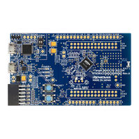
Target Board, 32-Bit MCU
Brand:
Renesas
| Category:
Motherboard
| Size: 1 MB
Table of Contents
Table of Contents
6
1 Overview
7
Package Components
7
Purpose
7
Features
7
Preparation
7
Target Board for RX23W: Table of Specifications
8
Block Diagram
9
2 Board Layout
10
3 Parts Layout
11
4 Operating Environment
12
5 User Circuits
13
Evaluation MCU
13
Bluetooth Low Energy
13
Emulator
14
USB-To-Serial Conversion
15
Act Led
15
Power LED
15
User Leds
15
External Power-Supply Header
16
Pmod Connector
17
Arduino uno Headers
18
Current Measurement Header
20
MCU Headers
20
Reset Switch
20
User Switch
20
Patterns for Cutting
20
6 Configurations
22
Modifying the Target Board for RX23W
22
Analog Power Supply
22
On-Chip Oscillator
23
7 Handling Precautions
24
Adding Load
24
Remodeling the Board
24
Limitation on the Number of Connected Target Boards for RX23W
24
8 Developing Code
25
Using the E 2 Studio
25
Using CS
26
9 Additional Information
27
10 Certification of Compliance
28
Radio-Related Laws
28
Advertisement
Renesas RX23W Series Quick Start Manual (18 pages)
Brand:
Renesas
| Category:
Motherboard
| Size: 1 MB
Table of Contents
Necessary Equipment
2
Operation Check
4
Revision History
16
Corporate Headquarters
18
Contact Information
18
Renesas RX23W Series Quick Start Manual (4 pages)
Brand:
Renesas
| Category:
Computer Hardware
| Size: 0 MB
Table of Contents
1. Installation
1
2. Connection
2
3. Importing Sample Code into E2 Studio
2
4. Programming and Debug
3
5. Next Step
4
6. Touch Demonstration Project
4
7. Renesas RX Compiler
4
8. User Manuals
4
9. Support
4
Advertisement
Related Products
Renesas RX Series
Renesas RX200 Series
Renesas RX23T Series
Renesas RTK5RX23W0C00000BJ
Renesas RE01 256KB
Renesas RA6M2
Renesas RC21012A
Renesas RC21211A
Renesas RC22308A
Renesas RC38612
Renesas Categories
Computer Hardware
Motherboard
Microcontrollers
Adapter
Switch
More Renesas Manuals
Login
Sign In
OR
Sign in with Facebook
Sign in with Google
Upload manual
Upload from disk
Upload from URL