Renesas RA4 Series Manuals
Manuals and User Guides for Renesas RA4 Series. We have 17 Renesas RA4 Series manuals available for free PDF download: User Manual, Quick Design Manual, Quick Start Manual, Engineering Manual
Renesas RA4 Series User Manual (1317 pages)
32-bit MCU
Brand: Renesas
|
Category: Microcontrollers
|
Size: 17 MB
Table of Contents
Advertisement

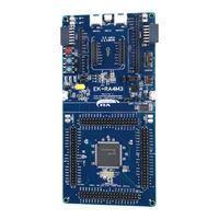
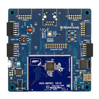
Renesas RA4 Series User Manual (45 pages)
Evaluation Kit for RA4L1 Microcontroller Group
Brand: Renesas
|
Category: Motherboard
|
Size: 3 MB
Table of Contents
Renesas RA4 Series Quick Design Manual (52 pages)
Brand: Renesas
|
Category: Microcontrollers
|
Size: 1 MB
Table of Contents
Advertisement

Renesas RA4 Series User Manual (36 pages)
Evaluation Kit for RA4E2 Microcontroller Group
Brand: Renesas
|
Category: Computer Hardware
|
Size: 1 MB
Table of Contents

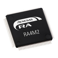
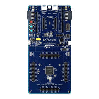
Renesas RA4 Series User Manual (36 pages)
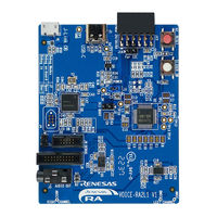
Evaluation Kit for RA4M2 Microcontroller Group
Brand: Renesas
|
Category: Motherboard
|
Size: 4 MB
Table of Contents
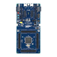
Renesas RA4 Series User Manual (35 pages)
Evaluation Kit for RA4M3 Microcontroller Group
Brand: Renesas
|
Category: Motherboard
|
Size: 4 MB
Table of Contents
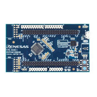
Renesas RA4 Series User Manual (29 pages)
Fast Prototyping Board for RA4E1 Microcontroller
Brand: Renesas
|
Category: Computer Hardware
|
Size: 1 MB
Table of Contents
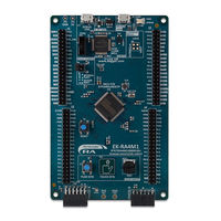
Renesas RA4 Series User Manual (38 pages)
Evaluation Kit for RA4M1 Microcontroller Group
Brand: Renesas
|
Category: Motherboard
|
Size: 2 MB
Table of Contents

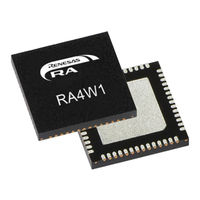
Renesas RA4 Series User Manual (26 pages)
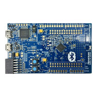
Evaluation Kit for RA4W1 Microcontroller Group
Brand: Renesas
|
Category: Motherboard
|
Size: 0 MB
Table of Contents

Renesas RA4 Series User Manual (31 pages)
Starter Kit Capacitive Touch Evaluation System
Brand: Renesas
|
Category: Computer Hardware
|
Size: 0 MB
Table of Contents

Renesas RA4 Series Quick Start Manual (32 pages)
Brand: Renesas
|
Category: Motherboard
|
Size: 1 MB
Table of Contents
Renesas RA4 Series Quick Start Manual (28 pages)
Evaluation Kit for RA4M3 Microcontroller Group
Brand: Renesas
|
Category: Motherboard
|
Size: 2 MB
Table of Contents

Renesas RA4 Series Quick Start Manual (28 pages)
Evaluation Kit for RA4E2 Microcontroller Group
Brand: Renesas
|
Category: Motherboard
|
Size: 1 MB
Table of Contents
Renesas RA4 Series Quick Start Manual (23 pages)
Evaluation Kit for RA4M1 Microcontroller Group
Brand: Renesas
|
Category: Motherboard
|
Size: 0 MB
Table of Contents
Renesas RA4 Series Quick Start Manual (24 pages)
Brand: Renesas
|
Category: Computer Hardware
|
Size: 1 MB
Table of Contents
Renesas RA4 Series Engineering Manual (17 pages)
Brand: Renesas
|
Category: Microcontrollers
|
Size: 0 MB
Table of Contents
Renesas RA4 Series Quick Start Manual (19 pages)
Evaluation Kit for RA4W1 Microcontroller Group
Brand: Renesas
|
Category: Motherboard
|
Size: 1 MB