Sign In
Upload
Manuals
Brands
Renesas Manuals
Motherboard
RA4W1
Renesas RA4W1 Manuals
Manuals and User Guides for Renesas RA4W1. We have
2
Renesas RA4W1 manuals available for free PDF download: User Manual, Application Note
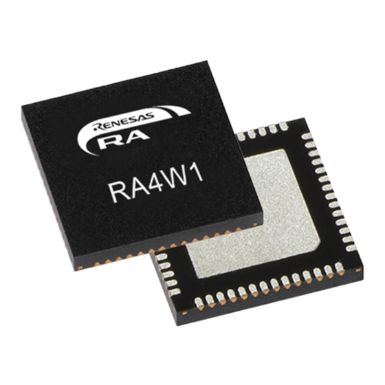
Renesas RA4W1 User Manual (1317 pages)
32-bit MCU
Brand:
Renesas
| Category:
Microcontrollers
| Size: 17 MB
Table of Contents
Table of Contents
9
Features
47
1 Overview
48
Function Outline
48
Block Diagram
54
Part Numbering
54
Function Comparison
56
Pin Functions
57
Pin Assignments
60
Pin Lists
61
2 Cpu
64
Overview
64
Debug
64
Operating Frequency
65
MCU Implementation Options
66
Trace Interface
66
JTAG/SWD Interface
67
Debug Mode
67
Debug Mode Definition
67
Debug Mode Effects
67
Low Power Mode
67
Reset
67
Programmers Model
68
Address Spaces
68
Cortex-M4 Peripheral Address Map
68
Coresight ROM Table
69
ROM Entries
69
Coresight Component Registers
69
DBGREG Module
70
Debug Status Register (DBGSTR)
70
Debug Stop Control Register (DBGSTOPCR)
71
Trace Control Register (TRACECTR)
71
DBGREG Coresight Component Registers
72
OCDREG Module
72
ID Authentication Code Register (IAUTH0 to 3)
72
MCU Status Register (MCUSTAT)
73
MCU Control Register (MCUCTRL)
74
OCDREG Coresight Component Registers
74
Coresight ATB Funnel
75
Flash Patch and Break Unit
75
Systick System Timer
75
Coresight Time Stamp Generator
75
OCD Emulator Connection
75
Dbgen
76
Unlock ID Code
76
Restrictions on Connecting an OCD Emulator
76
Starting Connection While in Low Power Mode
76
Changing Low Power Mode While in OCD Mode
76
Modifying the Unlock ID Code in OSIS
77
Connecting Sequence and JTAG/SWD Authentication
77
References
78
3 Operating Modes
79
Overview
79
Details of Operating Modes
79
Single-Chip Mode
79
SCI Boot Mode
79
USB Boot Mode
79
Operating Mode Transitions
79
Operating Mode Transitions as Determined by the Mode-Setting Pin
79
4 Address Space
80
Overview
80
5 Memory Mirror Function (MMF)
81
Overview
81
Register Descriptions
81
Memmirror Special Function Register (MMSFR)
81
Memmirror Enable Register (MMEN)
82
Operation
82
MMF Operation
82
Setting Example
86
6 Resets
87
Overview
87
Register Descriptions
90
Reset Status Register 0 (RSTSR0)
90
Reset Status Register 1 (RSTSR1)
91
Reset Status Register 2 (RSTSR2)
93
Operation
94
RES Pin Reset
94
Power-On Reset
94
Voltage Monitor Reset
95
Independent Watchdog Timer Reset
96
Watchdog Timer Reset
96
Software Reset
97
Determination of Cold/Warm Start
97
Determination of Reset Generation Source
97
7 Option-Setting Memory
99
Overview
99
Register Descriptions
99
Option Function Select Register 0 (OFS0)
99
Option Function Select Register 1 (OFS1)
102
MPU Registers
103
Access Window Setting Control Register (AWSC)
104
Access Window Setting Register (AWS)
105
Ocd/Serial Programmer ID Setting Register (OSIS)
106
Setting Option-Setting Memory
107
Allocation of Data in Option-Setting Memory
107
Setting Data for Programming Option-Setting Memory
107
Usage Note
108
Data for Programming Reserved Areas and Reserved Bits in the Option-Setting Memory
108
8 Low Voltage Detection (LVD)
109
Overview
109
Register Descriptions
111
Voltage Monitor 1 Circuit Control Register 1 (LVD1CR1)
111
Voltage Monitor 1 Circuit Status Register (LVD1SR)
111
Voltage Monitor Circuit Control Register (LVCMPCR)
112
Voltage Detection Level Select Register (LVDLVLR)
112
Voltage Monitor 1 Circuit Control Register 0 (LVD1CR0)
113
VCC Input Voltage Monitor
113
Monitoring Vdet0
113
Monitoring Vdet1
113
Reset from Voltage Monitor 0
114
Interrupt and Reset from Voltage Monitor 1
114
Event Link Output
116
Interrupt Handling and Event Linking
116
9 Clock Generation Circuit
117
Overview
117
Register Descriptions
120
System Clock Division Control Register (SCKDIVCR)
120
System Clock Source Control Register (SCKSCR)
122
PLL Clock Control Register 2 (PLLCCR2)
123
PLL Control Register (PLLCR)
123
Memory Wait Cycle Control Register (MEMWAIT)
124
Main Clock Oscillator Control Register (MOSCCR)
126
Sub-Clock Oscillator Control Register (SOSCCR)
127
Low-Speed On-Chip Oscillator Control Register (LOCOCR)
128
High-Speed On-Chip Oscillator Control Register (HOCOCR)
129
Middle-Speed On-Chip Oscillator Control Register (MOCOCR)
130
Oscillation Stabilization Flag Register (OSCSF)
130
Oscillation Stop Detection Control Register (OSTDCR)
132
Oscillation Stop Detection Status Register (OSTDSR)
133
Main Clock Oscillator Wait Control Register (MOSCWTCR)
134
High-Speed On-Chip Oscillator Wait Control Register (HOCOWTCR)
135
Main Clock Oscillator Mode Oscillation Control Register (MOMCR)
136
Sub-Clock Oscillator Mode Control Register (SOMCR)
136
Segment LCD Source Clock Control Register (SLCDSCKCR)
137
Clock out Control Register (CKOCR)
138
LOCO User Trimming Control Register (LOCOUTCR)
139
MOCO User Trimming Control Register (MOCOUTCR)
139
HOCO User Trimming Control Register (HOCOUTCR)
140
Trace Clock Control Register (TRCKCR)
140
USB Clock Control Register (USBCKCR)
141
Main Clock Oscillator
141
Connecting a Crystal Resonator
141
External Clock Input
142
Notes on External Clock Input
142
Sub-Clock Oscillator
142
Connecting a 32.768-Khz Crystal Resonator
142
Dedicated Clock Oscillator for Bluetooth
142
Connecting the Oscillator
142
Connecting the Bluetooth-Dedicated Clock Output Pin
143
Oscillation Stop Detection Function
143
Oscillation Stop Detection and Operation after Detection
143
Oscillation Stop Detection Interrupts
145
PLL Circuit
146
Internal Clock
146
System Clock (ICLK)
146
Peripheral Module Clock (PCLKA, PCLKB, PCLKC, PCLKD)
147
Flash Interface Clock (FCLK)
148
USB Clock (UCLK)
148
CAN Clock (CANMCLK)
148
CAC Clock (CACCLK)
148
RTC-Dedicated Clock (RTCSCLK, RTCLCLK)
148
IWDT-Dedicated Clock (IWDTCLK)
148
AGT-Dedicated Clock (AGTSCLK, AGTLCLK)
149
Systick Timer-Dedicated Clock (SYSTICCLK)
149
Segment LCDC Source Clock (LCDSRCCLK)
149
Clock/Buzzer Output Clock (CLKOUT)
149
JTAG Clock (JTAGTCK)
149
Clocks for BLE
149
Usage Notes
149
Notes on Clock Generation Circuit
149
Notes on Resonator
150
Notes on Board Design
150
Notes on Resonator Connect Pin
150
10 Clock Frequency Accuracy Measurement Circuit (CAC)
151
Overview
151
Register Descriptions
152
CAC Control Register 0 (CACR0)
152
CAC Control Register 1 (CACR1)
153
CAC Control Register 2 (CACR2)
154
CAC Interrupt Control Register (CAICR)
155
CAC Status Register (CASTR)
156
CAC Upper-Limit Value Setting Register (CAULVR)
157
CAC Lower-Limit Value Setting Register (CALLVR)
157
CAC Counter Buffer Register (CACNTBR)
157
Operation
157
Measuring Clock Frequency
157
Digital Filtering of Signals on CACREF Pin
158
Interrupt Requests
159
Usage Note
159
Settings for the Module-Stop Function
159
11 Low Power Modes
160
Overview
160
Register Descriptions
163
Standby Control Register (SBYCR)
163
Module Stop Control Register a (MSTPCRA)
164
Module Stop Control Register B (MSTPCRB)
164
Module Stop Control Register C (MSTPCRC)
166
Module Stop Control Register D (MSTPCRD)
167
Operating Power Control Register (OPCCR)
168
Sub Operating Power Control Register (SOPCCR)
168
Snooze Control Register (SNZCR)
169
Snooze End Control Register (SNZEDCR)
170
Snooze Request Control Register (SNZREQCR)
171
Flash Operation Control Register (FLSTOP)
173
Power Save Memory Control Register (PSMCR)
173
System Control OCD Control Register (SYOCDCR)
174
Reducing Power Consumption by Switching Clock Signals
174
Module-Stop Function
174
Function for Lower Operating Power Consumption
174
Setting Operating Power Control Mode
174
Operating Range
176
Sleep Mode
179
Transition to Sleep Mode
179
Canceling Sleep Mode
179
Software Standby Mode
180
Transition to Software Standby Mode
180
Canceling Software Standby Mode
181
Example of Software Standby Mode Application
181
Snooze Mode
183
Transition to Snooze Mode
183
Canceling Snooze Mode
183
Return to Software Standby Mode
184
Snooze Operation Example
186
Usage Notes
189
Register Access
189
I/O Port States
190
Module-Stop State of DMAC and DTC
190
Internal Interrupt Sources
190
Transition to Low Power Modes
190
Timing of WFI Instruction
191
Writing WDT/IWDT Registers by DMAC or DTC in Sleep Mode or Snooze Mode
191
Oscillators in Snooze Mode
191
Snooze Mode Entry by RXD0 Falling Edge
191
Using SCI0 in Snooze Mode
191
Conditions of A/D Conversion Start in Snooze Mode
191
Conditions of CTSU in Snooze Mode
191
ELC Event in Snooze Mode
191
Module-Stop Function for ADC140
192
Module-Stop Function for an Unused Circuit
192
12 Battery Backup Function
193
Overview
193
Features of Battery Backup Function
193
Battery Power Supply Switch
193
VBATT Pin Low Voltage Detection
193
VBATT_R Low Voltage Detection
193
Backup Registers
193
VBATT Wakeup Control Function
193
Time Capture Pin Detection
194
Register Descriptions
196
VBATT Control Register 1 (VBTCR1)
196
VBATT Control Register 2 (VBTCR2)
197
VBATT Status Register (VBTSR)
197
VBATT Comparator Control Register (VBTCMPCR)
198
VBATT Pin Low Voltage Detect Interrupt Control Register (VBTLVDICR)
199
VBATT Backup Register (Vbtbkrn) (N = 0 to 511)
199
VBATT Wakeup Control Register (VBTWCTLR)
199
VBATT Wakeup I/O 0 Output Trigger Select Register (VBTWCH0OTSR)
200
VBATT Input Control Register (VBTICTLR)
200
VBATT Output Control Register (VBTOCTLR)
201
VBATT Wakeup Trigger Source Enable Register (VBTWTER)
201
VBATT Wakeup Trigger Source Edge Register (VBTWEGR)
202
VBATT Wakeup Trigger Source Flag Register (VBTWFR)
202
Backup Register Access Control Register (BKRACR)
203
Operation
204
Battery Backup Function
204
VBATT Battery Power Supply Switch Usage
205
VBATT Pin Low Voltage Detection Procedures
206
VBATT Backup Register Usage
207
VBATT Wakeup Control Function Usage
207
Usage Notes
208
13 Register Write Protection
209
Overview
209
Register Descriptions
209
Protect Register (PRCR)
209
14 Interrupt Controller Unit (ICU)
210
Overview
210
Register Descriptions
211
IRQ Control Register I (Irqcri) (I = 0 to 4, 6, 7, 9, 11, 14, 15)
212
Non-Maskable Interrupt Status Register (NMISR)
213
Non-Maskable Interrupt Enable Register (NMIER)
215
Non-Maskable Interrupt Status Clear Register (NMICLR)
217
NMI Pin Interrupt Control Register (NMICR)
218
ICU Event Link Setting Register N (Ielsrn)
219
DMAC Event Link Setting Register N (Delsrn)
220
SYS Event Link Setting Register (SELSR0)
221
Wake up Interrupt Enable Register (WUPEN)
221
Vector Table
223
Interrupt Vector Table
223
Event Number
224
Interrupt Operation
229
Detecting Interrupts
229
Selecting Interrupt Request Destinations
230
CPU Interrupt Request
230
DTC Activation
230
DMAC Activation
231
Digital Filter
231
External Pin Interrupts
232
Non-Maskable Interrupt Operation
232
Return from Low Power Mode
233
Return from Sleep Mode
233
Return from Software Standby Mode
233
Return from Snooze Mode
233
Using the WFI Instruction with Non-Maskable Interrupts
234
Reference
234
15 Buses
235
Overview
235
Description of Buses
236
Main Buses
236
Slave Interface
236
Parallel Operation
236
Restriction on Endianness
237
Register Descriptions
237
Master Bus Control Register (Busmcnt<Master>)
237
Slave Bus Control Register (Busscnt<Slave>)
238
Bus Error Address Register (Busnerradd) (N = 1 to 4)
239
Bus Error Status Register (Busnerrstat) (N = 1 to 4)
239
Bus Error Monitoring Section
240
Error Type that Occurs by Bus
240
Operation When a Bus Error Occurs
240
Conditions Leading to Illegal Address Access Errors
241
Timeout
241
Notes on Using Flash Cache
242
References
242
16 Memory Protection Unit (MPU)
243
Overview
243
CPU Stack Pointer Monitor
243
Protection of Registers
246
Overflow/Underflow Error
246
Register Descriptions
246
Main Stack Pointer (MSP) Monitor Start Address Register (MSPMPUSA)
247
Main Stack Pointer (MSP) Monitor End Address Register (MSPMPUEA)
247
Process Stack Pointer (PSP) Monitor Start Address Register (PSPMPUSA)
248
Process Stack Pointer (PSP) Monitor End Address Register (PSPMPUEA)
248
Stack Pointer Monitor Operation after Detection Register (MSPMPUOAD, PSPMPUOAD)
249
Stack Pointer Monitor Access Control Register (MSPMPUCTL, PSPMPUCTL)
249
Stack Pointer Monitor Protection Register (MSPMPUPT, PSPMPUPT)
250
Arm MPU
251
Bus Master MPU
251
Register Descriptions
252
Group a Region N Start Address Register (Mmpusan) (N = 0 to 15)
253
Group a Region N End Address Register (Mmpuean) (N = 0 to 15)
253
Group a Region N Access Control Register (Mmpuacan) (N = 0 to 15)
253
Bus Master MPU Control Register (MMPUCTLA)
255
Group a Protection of Register (MMPUPTA)
256
Operation
256
Memory Protection
256
Protecting the Registers
258
Memory Protection Error
258
Bus Slave MPU
259
Register Descriptions
260
Access Control Register for Memory Bus 3 (SMPUMBIU)
260
Access Control Register for Internal Peripheral Bus 9 (SMPUFBIU)
260
Access Control Register for Memory Bus 4 (SMPUSRAM0)
261
Access Control Register for Internal Peripheral Bus 1 (SMPUP0BIU)
261
Access Control Register for Internal Peripheral Bus 3 (SMPUP2BIU)
262
Access Control Register for Internal Peripheral Bus 7 (SMPUP6BIU)
263
Slave MPU Control Register (SMPUCTL)
263
Functions
264
Memory Protection
264
Protecting the Registers
264
Memory Protection Error
264
Security MPU
264
Register Descriptions (Option-Setting Memory)
265
Security MPU Program Counter Start Address Register (Secmpupcsn) (N = 0, 1)
266
Security MPU Program Counter End Address Register (Secmpupcen) (N = 0, 1)
267
Security MPU Region 0 Start Address Register (SECMPUS0)
267
Security MPU Region 0 End Address Register (SECMPUE0)
268
Security MPU Region 1 Start Address Register (SECMPUS1)
268
Security MPU Region 1 End Address Register (SECMPUE1)
269
Security MPU Region 2 Start Address Register (SECMPUS2)
269
Security MPU Region 2 End Address Register (SECMPUE2)
270
Security MPU Region 3 Start Address Register (SECMPUS3)
270
Security MPU Region 3 End Address Register (SECMPUE3)
271
Security MPU Access Control Register (SECMPUAC)
271
Memory Protection
272
Notes on Debug
273
References
273
17 DMA Controller (DMAC)
274
Overview
274
Register Descriptions
276
DMA Source Address Register (DMSAR)
276
DMA Destination Address Register (DMDAR)
276
DMA Transfer Count Register (DMCRA)
277
DMA Block Transfer Count Register (DMCRB)
278
DMA Transfer Mode Register (DMTMD)
278
DMA Interrupt Setting Register (DMINT)
279
DMA Address Mode Register (DMAMD)
280
DMA Offset Register (DMOFR)
282
DMA Transfer Enable Register (DMCNT)
282
DMA Software Start Register (DMREQ)
283
DMA Status Register (DMSTS)
284
DMAC Module Activation Register (DMAST)
285
Operation
285
Transfer Mode
285
Extended Repeat Area Function
288
Address Update Function Using Offset
290
Activation Sources
294
Operation Timing
294
Execution Cycles of DMAC
295
Activating DMAC
295
Starting DMA Transfer
297
Registers During DMA Transfer
297
Channel Priority
298
Ending DMA Transfer
298
Transfer End by Completion of Specified Total Number of Transfer Operations
298
Transfer End by Repeat Size End Interrupt
298
Transfer End by Interrupt on Extended Repeat Area Overflow
298
Precautions for the End of DMA Transfer
299
Interrupts
299
Event Link
300
Low Power Consumption Function
300
Usage Notes
301
Access to Registers During DMA Transfer
301
DMA Transfer to Reserved Areas
301
Setting the DMAC Event Link Setting Register of the Interrupt Controller Unit (Icu.delsrn)
301
Suspending or Restarting DMA Activation
301
18 Data Transfer Controller (DTC)
302
Overview
302
Register Descriptions
303
DTC Mode Register a (MRA)
304
DTC Mode Register B (MRB)
304
DTC Transfer Source Register (SAR)
305
DTC Transfer Destination Register (DAR)
306
DTC Transfer Count Register a (CRA)
306
DTC Transfer Count Register B (CRB)
307
DTC Control Register (DTCCR)
307
DTC Vector Base Register (DTCVBR)
308
DTC Module Start Register (DTCST)
308
DTC Status Register (DTCSTS)
309
Activation Sources
309
Allocating Transfer Information and DTC Vector Table
310
Operation
311
Transfer Information Read Skip Function
313
Transfer Information Write-Back Skip Function
313
Normal Transfer Mode
314
Repeat Transfer Mode
315
Block Transfer Mode
316
Chain Transfer
317
Operation Timing
318
Execution Cycles of DTC
320
DTC Bus Mastership Release Timing
320
DTC Setting Procedure
320
Examples of DTC Usage
321
Normal Transfer
321
Chain Transfer
322
Chain Transfer When Counter = 0
324
Interrupt Source
325
Event Link
325
Snooze Control Interface
325
Module-Stop Function
325
18.11 Usage Notes
326
Transfer Information Start Address
326
19 Event Link Controller (ELC)
327
Overview
327
Register Descriptions
328
Event Link Controller Register (ELCR)
328
Event Link Software Event Generation Register N (Elsegrn) (N = 0, 1)
328
Event Link Setting Register N (Elsrn) (N = 0 to 9, 12, 14 to 18)
329
Operation
333
Relation between Interrupt Handling and Event Linking
333
Linking Events
333
Example of Procedure for Linking Events
333
Usage Notes
334
Linking DMAC or DTC Transfer End Signals as Events
334
Setting Clocks
334
Module-Stop Function Setting
334
ELC Delay Time
334
20 I/O Ports
335
Overview
335
Register Descriptions
336
Port Control Register 1 (PCNTR1/PODR/PDR)
336
Port Control Register 2 (PCNTR2/EIDR/PIDR)
337
Port Control Register 3 (PCNTR3/PORR/POSR)
338
Port Control Register 4 (PCNTR4/EORR/EOSR)
339
Port Mn Pin Function Select Register (Pmnpfs/Pmnpfs_Ha/Pmnpfs_By)
340
Write-Protect Register (PWPR)
342
Operation
342
General I/O Ports
342
Port Function Select
342
Port Group Function for the ELC
343
Behavior When ELC_PORT1, 2, 3, or 4 Is Input from the ELC
343
Behavior When an Event Pulse Is Output to the ELC
344
Handling of Unused Pins
345
Usage Notes
345
Procedure for Specifying the Pin Functions
345
Procedure for Using Port Group Input
345
Port Output Data Register (PODR) Summary
346
Notes on Using Analog Functions
346
I/O Buffer Specification
346
Selecting the USB_DP and USB_DM Pins
346
Pull-Up/Pull-Down Setting for P914 and P915 Using USBFS/GPIO Function
347
Peripheral Select Settings for each Product
347
21 Key Interrupt Function (KINT)
355
Overview
355
Register Descriptions
357
Key Return Control Register (KRCTL)
357
Key Return Flag Register (KRF)
357
Key Return Mode Register (KRM)
357
Operation
358
Operation When Not Using Key Interrupt Flag (KRMD = 0)
358
Operation When Using Key Interrupt Flag (KRMD = 1)
358
Usage Notes
360
22 Port Output Enable for GPT (POEG)
361
Overview
361
Register Descriptions
362
POEG Group N Setting Register (Poeggn) (N = A, B)
362
Output-Disable Control Operation
363
Pin Input Level Detection Operation
364
Digital Filter
364
Output-Disable Request from GPT
364
Output-Disable Control on Detection of Stopped Oscillation
364
Output-Disable Control Using Registers
364
Release from Output Disable
364
Interrupt Sources
365
External Trigger Output to GPT
365
Usage Notes
366
Transition to Software Standby Mode
366
Specifying Pins Associated with the GPT
366
23 General PWM Timer (GPT)
367
Overview
367
Register Descriptions
371
General PWM Timer Write-Protection Register (GTWP)
372
General PWM Timer Software Start Register (GTSTR)
372
General PWM Timer Software Stop Register (GTSTP)
373
General PWM Timer Software Clear Register (GTCLR)
373
General PWM Timer Start Source Select Register (GTSSR)
374
General PWM Timer Stop Source Select Register (GTPSR)
376
General PWM Timer Clear Source Select Register (GTCSR)
379
General PWM Timer up Count Source Select Register (GTUPSR)
381
General PWM Timer down Count Source Select Register (GTDNSR)
384
General PWM Timer Input Capture Source Select Register a(GTICASR)
386
General PWM Timer Input Capture Source Select Register B(GTICBSR)
389
General PWM Timer Control Register (GTCR)
391
General PWM Timer Count Direction and Duty Setting Register (GTUDDTYC)
393
General PWM Timer I/O Control Register (GTIOR)
395
General PWM Timer Interrupt Output Setting Register (GTINTAD)
398
General PWM Timer Status Register (GTST)
399
General PWM Timer Buffer Enable Register (GTBER)
403
General PWM Timer Counter (GTCNT)
404
General PWM Timer Compare Capture Register N (Gtccrn) (N = a to F)
405
General PWM Timer Cycle Setting Register (GTPR)
405
General PWM Timer Cycle Setting Buffer Register (GTPBR)
406
General PWM Timer Dead Time Control Register (GTDTCR)
406
General PWM Timer Dead Time Value Register U (GTDVU)
407
Output Phase Switching Control Register (OPSCR)
407
Operation
409
Basic Operation
409
Counter Operation
409
Waveform Output by Compare Match
415
Input Capture Function
418
Buffer Operation
420
GTPR Register Buffer Operation
420
Buffer Operation for GTCCRA and GTCCRB
423
PWM Output Operating Mode
428
Saw-Wave PWM Mode
428
Saw-Wave One-Shot Pulse Mode
431
Triangle-Wave PWM Mode 1 (32-Bit Transfer at Trough)
433
Triangle-Wave PWM Mode 2 (32-Bit Transfer at Crest and Trough)
436
Triangle-Wave PWM Mode 3 (64-Bit Transfer at Trough)
438
Automatic Dead Time Setting Function
440
Count Direction Changing Function
444
Function of Output Duty 0% and 100
445
Hardware Count Start/Count Stop and Clear Operation
447
Hardware Start Operation
447
Hardware Stop Operation
448
Hardware Clear Operation
451
Synchronized Operation
454
Synchronized Operation by Software
454
Synchronized Operation by Hardware
456
PWM Output Operation Examples
458
Phase Counting Function
464
Output Phase Switching (GPT_OPS)
471
Input Selection and Synchronization of External Input Signal
474
Input Sampling
475
Input Phase Decode
475
Output Selection Control
475
Output Selection Control (Group Output Disable Function)
477
Event Link Controller (ELC) Output
477
GPT_OPS Start Operation Setting Flow
478
Interrupt Sources
478
DMAC/DTC Activation
482
Operations Linked by ELC
482
Event Signal Output to ELC
482
Event Signal Inputs from ELC
482
Noise Filter Function
482
Protection Function
483
Write-Protection for Registers
483
Disabling of Buffer Operation
483
GTIOC Pin Output Negate Control
484
Initialization Method of Output Pins
485
Pin Settings after Reset
485
Pin Initialization Due to Error During Operation
486
Usage Notes
486
Module-Stop Function Setting
486
Gtccrn Settings During Compare Match Operation (N = a to F)
486
Setting Range for GTCNT Counter
487
Starting and Stopping the GTCNT Counter
487
Priority Order of each Event
487
24 Asynchronous General Purpose Timer (AGT)
489
Overview
489
Register Descriptions
491
AGT Counter Register (AGT)
491
AGT Compare Match a Register (AGTCMA)
491
AGT Compare Match B Register (AGTCMB)
492
AGT Control Register (AGTCR)
492
AGT Mode Register 1 (AGTMR1)
494
AGT Mode Register 2 (AGTMR2)
495
AGT I/O Control Register (AGTIOC)
495
AGT Event Pin Select Register (AGTISR)
496
AGT Compare Match Function Select Register (AGTCMSR)
497
AGT Pin Select Register (AGTIOSEL)
497
Operation
498
Reload Register and Counter Rewrite Operation
498
Reload Register and Compare Register A/B Rewrite Operation
499
Timer Mode
500
Pulse Output Mode
501
Event Counter Mode
502
Pulse Width Measurement Mode
503
Pulse Period Measurement Mode
504
Compare Match Function
505
Output Settings for each Mode
507
Standby Mode
507
Interrupt Sources
508
Event Signal Output to ELC
508
Usage Notes
508
Count Operation Start and Stop Control
508
Access to Counter Register
509
When Changing Mode
509
Digital Filter
509
How to Calculate Event Number, Pulse Width, and Pulse Period
509
When Count Is Forcibly Stopped by TSTOP Bit
510
When Selecting AGT0 Underflow as the Count Source
510
Reset of I/O Register
510
When Selecting PCLKB, PCLKB/8, or PCLKB/2 as the Count Source
510
When Selecting AGTLCLK or AGTSCLK as the Count Source
510
When Switching Source Clock
510
25 Realtime Clock (RTC)
511
Overview
511
Register Descriptions
513
64-Hz Counter (R64CNT)
513
Second Counter (Rseccnt)/Binary Counter 0 (BCNT0)
513
Minute Counter (Rmincnt)/Binary Counter 1 (BCNT1)
514
Hour Counter (Rhrcnt)/Binary Counter 2 (BCNT2)
515
Day-Of-Week Counter (Rwkcnt)/Binary Counter 3 (BCNT3)
516
Day Counter (RDAYCNT)
517
Month Counter (RMONCNT)
517
Year Counter (RYRCNT)
518
Second Alarm Register (Rsecar)/Binary Counter 0 Alarm Register (BCNT0AR)
518
Minute Alarm Register (Rminar)/Binary Counter 1 Alarm Register (BCNT1AR)
519
Hour Alarm Register (Rhrar)/Binary Counter 2 Alarm Register (BCNT2AR)
520
Day-Of-Week Alarm Register (Rwkar)/Binary Counter 3 Alarm Register (BCNT3AR)
521
Date Alarm Register (Rdayar)/Binary Counter 0 Alarm Enable Register (BCNT0AER)
522
Month Alarm Register (Rmonar)/Binary Counter 1 Alarm Enable Register (BCNT1AER)
523
Year Alarm Register (Ryrar)/Binary Counter 2 Alarm Enable Register (BCNT2AER)
524
Year Alarm Enable Register (Ryraren)/Binary Counter 3 Alarm Enable Register (BCNT3AER)
525
RTC Control Register 1 (RCR1)
526
RTC Control Register 2 (RCR2)
527
RTC Control Register 4 (RCR4)
530
Frequency Register (RFRH/RFRL)
531
Time Error Adjustment Register (RADJ)
532
Time Capture Control Register 0 (RTCCR0)
532
Second Capture Register 0 (RSECCP0) /BCNT0 Capture Register 0
534
(Bcnt0Cp0)
534
Minute Capture Register 0 (RMINCP0)/BCNT1 Capture Register 0 (BCNT1CP0)
534
Hour Capture Register 0 (RHRCP0) /BCNT2 Capture Register 0 (BCNT2CP0)
535
Date Capture Register 0 (RDAYCP0) /BCNT3 Capture Register 0 (BCNT3CP0)
536
Month Capture Register 0 (RMONCP0)
537
Operation
537
Outline of Initial Settings of Registers after Power on
537
Clock and Count Mode Setting Procedure
537
Setting the Time
538
30-Second Adjustment
539
Reading 64-Hz Counter and Time
540
Alarm Function
541
Procedure for Disabling Alarm Interrupt
541
Time Error Adjustment Function
542
Automatic Adjustment
542
Adjustment by Software
543
Procedure for Changing the Mode of Adjustment
543
Procedure for Stopping Adjustment
544
Capturing the Time
544
Interrupt Sources
545
Event Link Output
546
Interrupt Handling and Event Linking
547
Usage Notes
547
Register Writing During Counting
547
Use of Periodic Interrupts
547
RTCOUT (1-Hz/64-Hz) Clock Output
548
Transitions to Low Power Modes after Setting Registers
548
Notes on Writing to and Reading from Registers
548
Changing the Count Mode
548
Initialization Procedure When the RTC Is Not to be Used
548
When Switching Source Clock
549
26 Watchdog Timer (WDT)
550
Overview
550
Register Descriptions
551
WDT Refresh Register (WDTRR)
551
WDT Control Register (WDTCR)
552
WDT Status Register (WDTSR)
554
WDT Reset Control Register (WDTRCR)
555
WDT Count Stop Control Register (WDTCSTPR)
556
Option Function Select Register 0 (OFS0)
556
Operation
556
Count Operation in each Start Mode
556
Register Start Mode
556
Auto Start Mode
558
Controlling Writes to the WDTCR, WDTRCR, and WDTCSTPR Registers
559
Refresh Operation
560
Reset Output
561
Interrupt Sources
561
Reading the Down-Counter Value
561
Associations between Option Function Select Register 0 (OFS0) and WDT Registers
562
Link Operation by ELC
562
Usage Notes
562
ICU Event Link Setting Register N (Ielsrn) Setting
562
27 Independent Watchdog Timer (IWDT)
563
Overview
563
Register Descriptions
564
IWDT Refresh Register (IWDTRR)
564
IWDT Status Register (IWDTSR)
565
Option Function Select Register 0 (OFS0)
566
Operation
568
Auto Start Mode
568
Refresh Operation
569
Status Flags
570
Reset Output
571
Interrupt Sources
571
Reading the Down-Counter Value
571
Link Operation by ELC
571
Usage Notes
572
Refresh Operations
572
Clock Division Ratio Setting
572
28 USB 2.0 Full-Speed Module (USBFS)
573
Overview
573
Register Descriptions
575
System Configuration Control Register (SYSCFG)
575
System Configuration Status Register 0 (SYSSTS0)
576
Device State Control Register 0 (DVSTCTR0)
577
CFIFO Port Register (CFIFO/CFIFOL)
579
D0FIFO Port Register (D0FIFO/D0FIFOL)
579
D1FIFO Port Register (D1FIFO/D1FIFOL)
579
CFIFO Port Select Register (CFIFOSEL)
581
D0FIFO Port Select Register (D0FIFOSEL)
581
D1FIFO Port Select Register (D1FIFOSEL)
581
CFIFO Port Control Register (CFIFOCTR)
584
D0FIFO Port Control Register (D0FIFOCTR)
584
D1FIFO Port Control Register (D1FIFOCTR)
584
Interrupt Enable Register 0 (INTENB0)
585
Interrupt Enable Register 1 (INTENB1)
586
BRDY Interrupt Enable Register (BRDYENB)
587
NRDY Interrupt Enable Register (NRDYENB)
588
BEMP Interrupt Enable Register (BEMPENB)
588
SOF Output Configuration Register (SOFCFG)
589
Interrupt Status Register 0 (INTSTS0)
590
Interrupt Status Register 1 (INTSTS1)
592
BRDY Interrupt Status Register (BRDYSTS)
595
NRDY Interrupt Status Register (NRDYSTS)
595
BEMP Interrupt Status Register (BEMPSTS)
596
Frame Number Register (FRMNUM)
597
USB Request Type Register (USBREQ)
598
USB Request Value Register (USBVAL)
598
USB Request Index Register (USBINDX)
599
USB Request Length Register (USBLENG)
600
DCP Configuration Register (DCPCFG)
600
DCP Maximum Packet Size Register (DCPMAXP)
601
DCP Control Register (DCPCTR)
602
Pipe Window Select Register (PIPESEL)
605
Pipe Configuration Register (PIPECFG)
606
Pipe Maximum Packet Size Register (PIPEMAXP)
608
Pipe Cycle Control Register (PIPEPERI)
609
Pipen Control Registers (Pipenctr) (N = 1 to 9)
610
Pipen Transaction Counter Enable Register (Pipentre) (N = 1 to 5)
616
Pipen Transaction Counter Register (Pipentrn) (N = 1 to 5)
617
Device Address N Configuration Register (Devaddn) (N = 0 to 5)
618
USB Module Control Register (USBMC)
618
BC Control Register 0 (USBBCCTRL0)
619
Operation
620
System Control
620
Setting Data to the USBFS-Related Registers
620
Selecting the Controller Function
620
Controlling the USBFS Data Bus Using Resistors
620
Example of USB External Connection Circuits
621
Interrupt Sources
625
Interrupt Descriptions
629
BRDY Interrupt
629
NRDY Interrupt
632
BEMP Interrupt
634
Device State Transition Interrupt (Device Controller Mode)
635
Control Transfer Stage Transition Interrupt (Device Controller Mode)
636
Frame Update Interrupt
637
VBUS Interrupt
637
Resume Interrupt
638
OVRCR Interrupt
638
BCHG Interrupt
638
DTCH Interrupt
638
SACK Interrupt
638
SIGN Interrupt
638
ATTCH Interrupt
638
EOFERR Interrupt
638
Portable Device Detection Interrupt
639
Pipe Control
639
Pipe Control Register Switching Procedures
639
Transfer Types
640
Endpoint Number
640
Maximum Packet Size Setting
640
Transaction Counter for Pipes 1 to 5 in the Receiving Direction
640
Response PID
641
Data PID Sequence Bit
642
Response PID = NAK Function
642
Auto Response Mode
642
OUT-NAK Mode
642
Null Auto Response Mode
643
FIFO Buffer Memory
643
FIFO Buffer Clearing
643
FIFO Port Functions
644
DMA Transfers (D0FIFO and D1FIFO Ports)
645
Control Transfers Using DCP
645
Control Transfers in Host Controller Mode
646
Control Transfers in Device Controller Mode
646
Bulk Transfers (Pipes 1 to 5)
647
Interrupt Transfers (Pipes 6 to 9)
647
Interval Counter for Interrupt Transfers in Host Controller Mode
648
Isochronous Transfers (Pipes 1 and 2)
648
Error Detection in Isochronous Transfers
648
Data-Pid
649
Interval Counter
649
SOF Interpolation Function
655
Pipe Schedule
655
Conditions for Generating Transactions
655
Transfer Schedule
656
Enabling USB Communication
656
Battery Charging Detection Processing
656
Processing in Device Controller Mode
656
Processing When Host Controller Is Selected
658
Usage Notes
661
Settings for the Module-Stop State
661
Clearing the Interrupt Status Register on Exiting Software Standby Mode
661
Clearing the Interrupt Status Register after Setting up the Port Function
661
Advertisement
Renesas RA4W1 Application Note (20 pages)
Guidelines for 2.4 GHz Wireless Board Design
Brand:
Renesas
| Category:
Motherboard
| Size: 0 MB
Table of Contents
Table of Contents
1
Overview
3
Related Documents
3
Board Design Guidelines
4
Pin List of the RF Transceiver Unit
4
Oscillator Circuit for the Wireless-Dedicated (Bluetooth-Dedicated) Clock
5
Antenna Connection Pin
7
Impedance of the Signal Line Form an Antenna to the "ANT" Pin
7
RF Filter for Spurious Emissions Reduction
8
Power Supply Mode for the RF Transceiver
10
DC-DC Converter Mode
10
Linear Regulator Mode
12
Power Supply and Ground Patterns
14
Power Supply
14
Ground
14
Circuit Diagram for Reference
16
Parts List for Reference
17
Revision History
18
Advertisement
Related Products
Renesas RA4 Series
Renesas RA4M2
Renesas RA4M3
Renesas RA6M2
Renesas RAJ306102
Renesas RAA214020
Renesas RA8E1 Series
Renesas RAA223011
Renesas RAA211803
Renesas RAA211403
Renesas Categories
Computer Hardware
Motherboard
Microcontrollers
Adapter
Switch
More Renesas Manuals
Login
Sign In
OR
Sign in with Facebook
Sign in with Google
Upload manual
Upload from disk
Upload from URL