Sign In
Upload
Manuals
Brands
Motorola Manuals
Two-Way Radio
ASTRO SRX 2200 Series
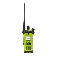
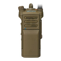
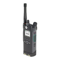
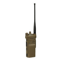
Motorola ASTRO SRX 2200 Series Manuals
Manuals and User Guides for Motorola ASTRO SRX 2200 Series. We have
6
Motorola ASTRO SRX 2200 Series manuals available for free PDF download: Service Manual, User Manual, Quick Reference Manual, Quick Reference Card
Motorola ASTRO SRX 2200 Series Service Manual (438 pages)
Brand:
Motorola
| Category:
Two-Way Radio
| Size: 29.88 MB
Table of Contents
Foreword
4
Manual Revisions
4
Product Safety and Rf Exposure Compliance
4
Computer Software Copyrights
4
Document Copyrights
4
Disclaimer
4
Trademarks
4
Document History
5
Table of Contents
7
List of Tables
10
List of Figures
12
Commercial Warranty
17
Limited Warranty
17
Motorola Communication Products
17
Chapter 1 Introduction
21
General
21
Notations Used in this Manual
22
Chapter 2 Radio Power
23
General
23
Table 2-1. Batteries
23
DC Power Routing - Transceiver Board
24
Figure 2-1. DC Power Distribution
24
DC Power Routing - VOCON Board
25
Table 2-2. Transceiver Voltage Regulators
25
Chapter 3 Theory of Operation
27
Figure 3-1. APX 5000/ APX 6000/ APX 6000XE/ SRX 2200 Overall Block Diagram
28
Figure 3-2. Transceiver (VHF) Block Diagram (Power and Control Omitted)
29
Transceiver Board
29
Figure 3-3. Transceiver (UHF1 and UHF2) Block Diagram (Power and Control Omitted)
30
Figure 3-4. Transceiver (7/800) Block Diagram (Power and Control Omitted)
30
Table 3-1. Battery Connector M101
31
Table 3-2. VOCON Connector J1001
31
Figure 3-5. Receiver Block Diagram (VHF)
33
Figure 3-6. Receiver Block Diagram (UHF1 and UHF2)
34
Figure 3-7. Receiver Block Diagram (7/800)
34
Figure 3-8. Transmitter Block Diagram (VHF)
37
Figure 3-9. Transmitter Block Diagram (UHF1 and UHF2)
37
Figure 3-10. Transmitter Block Diagram (7/800)
38
Directional Coupler
39
Antenna Switch
40
Harmonic Filter
40
Figure 3-11. Synthesizer Block Diagram (VHF)
43
Figure 3-12. Synthesizer Block Diagram (UHF1 and UHF2)
43
Figure 3-13. Synthesizer Block Diagram (7/800)
44
Table 3-3. Port Expander Pin Settings
46
Controller
50
Figure 3-14. Controller Interconnection Diagram
50
Figure 3-15. Controller Electrical Overview
52
Figure 3-16. Controller DC Block Diagram
53
Table 3-4. DC Supplies and Sources for Controller
54
Table 3-5. Mako's LDO and Supplies
55
Figure 3-17. V_SW_1.4 Switched Power Supply
56
Figure 3-18. 5V Switched Power Supply
57
Table 3-6. Pulse Switching Combination
57
Figure 3-19. Power-Up Timing Regulators
58
Figure 3-20. VOCON Clock Architecture
59
Table 3-7. VOCON Clock Distribution
59
Figure 3-21. Overview of OMAP Interconnection with VOCON Peripherals
60
Figure 3-22. OMAP Memory Interface
61
Figure 3-23. Timing of Power-Up and Initialization of Emmc
63
Figure 3-24. Emmc Topography
64
Figure 3-25. Block Diagram of VOCON and EXPANSION Boards as Related to Emmc
65
Figure 3-26. RX / TX SSI Configuration
66
Figure 3-27. Audio SSI Configuration
66
Figure 3-28. SPI and I2C Configuration
67
Figure 3-29. CPLD Block Diagram
68
Figure 3-30. Audio TX Path Block Diagram
69
Figure 3-31. VOCON RX Audio Path Block Diagram
70
Figure 3-32. Control Top Block Diagram
71
Figure 3-33. Display Circuit Detail Overview Block Diagram
72
Table 3-8. Color Schemes
74
Figure 3-34. Lighting Controller Overview
75
Figure 3-35. Lighting Controller - SRX 2200
76
Figure 3-36. Keypad Interface Outline
77
Table 3-9. Key Map Matrix
77
Side Controls
78
Figure 3-37. GCAI Signal Configuration
79
Figure 3-38. GCAI Connector
79
Table 3-11. GCAI Connector Pin Assignment
80
Figure 3-39. GCAI Connector - Back View
81
Figure 3-40. VOCON to RF Board Interface
82
Figure 3-41. APX 5000/ APX 6000/ APX 6000XE/ SRX 2200 Encryption Architecture
83
Table 3-12. Encryption Algorithms and Corresponding Kit Numbers
84
Global Positioning Sytem (GPS)
86
Figure 3-42. GPS Block Diagram (VHF/700-800 Mhz)
87
Table 3-13. Power and I/O Pins for NI5500
87
Accelerometer
88
Figure 3-43. GPS Block Diagram (UHF1 and UHF2)
88
Figure 3-44. Directions of the Detectable Accelerations
88
Figure 3-45. Accelerometer Block Diagram
89
Table 3-14. SPI Interface
89
Table 3-15. Register Address Map
90
Bluetooth
91
Figure 3-46. Relation of Bluetooth Antenna Assembly to Expansion Board
91
Figure 3-47. Bluetooth Connection Flowchart
92
Figure 3-48. Bluetooth/Controller Interface with Clock Sources
93
Figure 3-49. Bluetooth Functional Block Diagram
93
Figure 3-50. Bluetooth Low-Frequency Circuit Block Diagram
94
Figure 3-51. Bluetooth Low-Frequency Pairing Data Path
94
Figure 3-52. Detailed Low-Frequency Transmit/Receive Paths
95
Figure 3-53. Chip Power-Up/Power-Down Sequence (Exernal Input/Output Shown)
95
Figure 3-54. Current Distribution Tree for Bluetooth Circuitry
96
Figure 3-55. Bluetooth LF UART Connection Block Diagram
97
Table 3-16. Bluetooth Host Processor UART I/O
97
Table 3-17. SPI I/O
98
Table 3-18. USB I/O
98
Figure 3-56. Bluetooth USB Interface too Main VOCON
99
Table 3-19. GPIO I/O
99
Chapter 4 Troubleshooting Procedures
101
Handling Precautions
101
Recommended Service Tools
102
Table 4-1. Recommended Service Tools
102
Standard Bias Table
103
Table 4-2. Standard Operating Bias - DC Voltages
103
Table 4-3. Standard Operating Bias - Clock Sources
103
Power-Up Self-Check Errors
104
Table 4-4. Power-Up Self-Check Error Codes
104
Power-Up Self-Check Diagnostics and Repair (Not for Field Use)
105
Table 4-5. Power-Up Self-Check Diagnostic Actions
105
Chapter 5 Troubleshooting Charts
107
List of Troubleshooting Charts
107
Table 5-1. Troubleshooting Charts
107
Main Troubleshooting Flowchart
109
Power-Up Failure
111
DC Supply Failure
121
Top/CID Display Failure
128
Main Display Failure
129
Volume Set Error
130
Channel Select Error
131
Keypad Error
132
5.10 Side Button Error
133
VOCON RX Audio Error
134
VOCON RX Audio Error
135
VOCON TX Audio Error
136
5.15 Keyload Failure
138
5.16 Secure Hardware Failure
139
5.17 Emmc Memory Failure
140
RX RF Failure
141
5.19 FGU Failure
152
5.20 FGU Power Failure
153
5.21 GPS Failure
154
Bluetooth Failure
156
PA Failure
162
Chapter 6 Troubleshooting Waveforms
173
List of Waveforms
173
Table 6-1. List of Waveforms
173
Clocks
175
Figure 6-1. 32 Khz Clock Waveform
175
Figure 6-2. 4 Mhz Clock Waveform
176
Figure 6-3. 12 Mhz Clock Waveform
177
Figure 6-4. 16.8 Mhz Clock Waveform
178
Figure 6-5. 24 Mhz Clock Waveform
179
Audio SSI
180
Figure 6-6. Audio SSI - Red Tx Waveform
180
Figure 6-7. Audio SSI - Red Rx Waveform
181
Figure 6-8. Audio SSI - Sync. Waveform
182
Figure 6-9. Audio SSI - BCLK. Waveform
183
Rx Ssi
184
Figure 6-10. RX SSI - CLK. Waveform
184
Figure 6-11. RX SSI - da Waveform
185
Figure 6-12. RX SSI - Fsync. Waveform
186
Tx Ssi
187
Figure 6-13. TX SSI - TX CLK. Waveform
187
Figure 6-14. TX SSI - da Waveform
188
Figure 6-15. TX SSI - Fsync. Waveform
189
Spi
190
Figure 6-16. SPI - CLK Waveform
190
Figure 6-17. MOSI Waveform
191
Figure 6-18. MISO Waveform
192
Figure 6-19. CS Waveform
193
I2C Bus
194
Figure 6-20. I2C Bus - SCA Waveform
194
Figure 6-21. I2C Bus - SCA 5V Waveform
195
Figure 6-22. I2C Bus - SDA Waveform
196
One Wire
197
Figure 6-23. 1-Wire Waveform
197
Gcai
198
Figure 6-24. GCAI - GPIO0 Waveform
198
Figure 6-25. GCAI - GPIO4 Waveform
199
6.10 Usb
200
Figure 6-26. USB - D- Waveform
200
Figure 6-27. USB - D+ Waveform
201
6.11 Uart
202
Figure 6-28. UART - RX Waveform
202
Figure 6-29. UART - TX Waveform
203
6.12 Sdram
204
Figure 6-30. SDRAM - CLK Waveform
204
Figure 6-31. SDRAM - CLKX Waveform
205
6.13 Flash Control
206
Figure 6-32. FLASH CONTROL - ADV Waveform
206
Figure 6-33. FLASH CONTROL - CS3 Waveform
207
Figure 6-34. FLASH CONTROL - OE Waveform
208
Figure 6-35. FLASH CONTROL - RDY Waveform
209
Figure 6-36. FLASH CONTROL - WE Waveform
210
Expandable Memory (Emmc)
211
Figure 6-37. Emmc: Power-On until Final Initialization Waveforms
211
Figure 6-38. Emmc: Correct Detection, Configuration and Initialization Waveforms
212
Figure 6-39. Emmc: Failure to Properly Detect, Configure and Initialize Waveforms
213
Figure 6-40. MMC_CLK @ < 400 Khz During "Clock Frequency Identification Mode
214
Figure 6-41. MMC_CLK @ < 24 Mhz During "Clock Frequency Data Transfer Mode
215
Figure 6-42. MMC_CMD Actual Waveform When Probing with Active Probes; Short Wires; GND Pin Soldered
216
Figure 6-43. MMC_CMD Misleading Waveform When Probing with Passive Probe; Long Wires; GND Clip
217
Figure 6-44. MMC_DAT0, MMC_DAT1, MMC_DAT2, MMC_DAT3 Data Lines During Data Transmission between Emmc and OMAP
218
Figure 6-45. F2_TIMER_OUT Clock from CPLD into OMAP for Emmc Operation
219
6.15 Receive Baseband Signals
220
Figure 6-46. Received Baseband Waveforms
220
6.16 Gps
221
Figure 6-47. GPS TCXO Waveforms
221
Figure 6-48. GPS RTC Waveforms
222
Figure 6-49. GPS UART DATA Waveforms
223
6.17 Bluetooth Troubleshooting Waveforms
224
Table 6-2. Bluetooth Command to TX
224
Table 6-3. Bluetooth Command to RX
225
Table 6-4. Low Frequency Command to TX
225
Table 6-5. Low Frequency Command to RX
225
Table 6-6. Bluetooth Test Points
226
Figure 6-50. Startup Waveforms - Vmax of TP16
227
Figure 6-51. Startup - Timing Difference of TP9 to TP16
228
Figure 6-52. Startup - Timing Difference of TP5 to TP16 and Voltage Statistics
229
Figure 6-53. Startup - Timing Difference of TP4 to TP16 and Time Statistics
230
Figure 6-54. Startup - Timing Difference of TP4 to TP5 and Time Statistics
231
Figure 6-55. Startup - Vmax of TP5 and Time Statistics
232
Figure 6-56. Startup - Vmax of TP4 and Time Statistics
233
Figure 6-57. Startup - Vmax of TP5 and Voltage Statistics
234
Figure 6-58. Startup - Vmax of TP9 and Voltage Statistics
235
Figure 6-59. Startup - Vmax of TP10 and Time Statistics
236
Figure 6-60. Startup - Vmax of TP16 and Voltage Statistics
237
Figure 6-61. Startup - Vmax of TP13 and Voltage Statistics
238
Figure 6-62. Startup - Vmax of TP11 and Voltage Statistics
239
Figure 6-63. Startup - Timing Difference of TP13 to TP16 and Time Statistics
240
Figure 6-64. Startup - Timing Difference of TP10 to TP13 and Time Statistics
241
Figure 6-65. Startup - Timing Difference of TP11 to TP13 and Time Statistics
242
Figure 6-66. Bluetooth CW on Spectrum Analyzer
243
6.18 Bluetooth Steady-State
244
Figure 6-67. Expansion Board - USB D+ Vmax and Packet Timing with Statistics
244
Figure 6-68. Expansion Board - USB D- Vmax and Packet Timing with Statistics
245
Figure 6-69. Expansion Board - VSW_3.6 Voltage Statistics
246
Figure 6-70. Expansion Board - 32 Khz Clock Vmax with Statistics
247
Figure 6-71. Expansion Board - LF Coil with TX and RX Waveform Measured by a Conducted Cable on LF Coil
248
6.19 LF CW on Spectrum Analyzer
249
Figure 6-72. LF CW on Spectrum Analyzer
249
Chapter 7 Troubleshooting Tables
251
List of Board and IC Signals
251
Table 7-2. VOCON Board to RF Board Connector Interface PIN-OUT
252
Table 7-3. VOCON Board to EXPANSION Board Connector Interface PIN-OUT
254
Table 7-4. VOCON Board to Control Top with Top Display Interface PIN-OUT
257
Table 7-5. VOCON Board to Front Display Interface PIN-OUT
259
Table 7-6. VOCON Board to Keypad Interface PIN-OUT
260
Table 7-7. EXPANSION Board to Accessory Connector (GCAI) Interface PIN-OUT
261
Table 7-8. EXPANSION Board to Side Buttons Interface PIN-OUT
262
Table 7-9. EXPANSION Board to Speaker and Microphones Interface PIN-OUT
263
Table 7-10. EXPANSION Board to AVR / JTAG Interface PIN-OUT
264
Table 7-11. Primary IC Reference Designators
265
Table 7-12. Overall GPIO Pin Functions Across Multiple Boards
266
Chapter 8 Schematics, Boards Overlays, and Parts Lists
277
List of Transceiver Schematics and Board Overlays
277
Table 8-1. List of Transceiver Schematics and Board Overlays
277
List of VOCON Schematics and Board Overlays
278
List of Expansion Board Schematics and Overlays
278
Table 8-2. List of VOCON Schematics and Board Overlays
278
Table 8-3. List of VOCON Schematics and Board Overlays
278
Transceiver (RF) Boards: VHF
279
Figure 8-1. NUD7120A Transceiver (RF) Board Overall Circuit Schematic
279
Figure 8-2. NUD7120A Harmonic Filter Circuit
280
Figure 8-3. NUD7120A GPS Circuit
281
Figure 8-4. NUD7120A Miscellaneous Connector Circuit
282
Figure 8-5. NUD7120A Receiver Front End Circuit
283
Figure 8-6. NUD7120A Receiver Back End Circuit
284
Figure 8-7. NUD7120A DC Power Circuit
285
Figure 8-8. NUD7120A Transmitter and Automatic Level Control Circuits
286
Figure 8-9. NUD7120A Frequency Generation Unit (Synthesizer) Circuit – 1 of 2
287
Figure 8-10. NUD7120A Frequency Generation Unit (VCO) Circuit – 2 of 2
288
Figure 8-11. NUD7120A Mixer and if Filter Circuits
289
Figure 8-12. NUD7120A Power Amplifier Circuit
290
Figure 8-13. NUD7120A Transceiver (RF) Board Layout – Side 1
291
Figure 8-14. NUD7120A Transceiver (RF) Board Layout – Side 2
292
Transceiver (RF) Boards: UHF1
301
Figure 8-15. NUE7365A/ NUE7369A Transceiver (RF) Board Overall Circuit Schematic
301
Figure 8-16. NUE7365A/ NUE7369A UHF1 Harmonic Filter Circuit
302
Figure 8-17. NUE7365A/ NUE7369A GPS Circuit
303
Figure 8-18. NUE7365A/ NUE7369A Miscellaneous Connector Circuit
304
Figure 8-19. NUE7365A Receiver Front End Circuit
305
Figure 8-20. NUE7365A/ NUE7369A Receiver Back End Circuit
306
Figure 8-21. NUE7365A/ NUE7369A DC Power Circuit
307
Figure 8-22. NUE7365A/ NUE7369A Transmitter and Automatic Level Control Circuits
308
Figure 8-23. NUE7365A Frequency Generation Unit (Synthesizer) Circuit – 1 of 2
309
Figure 8-24. NUE7365A Frequency Generation Unit (VCO) Circuit – 2 of 2
310
Figure 8-25. NUE7365A/ NUE7369A Mixer and if Filter Circuits
311
Figure 8-26. NUE7365A Power Amplifier Circuit
312
Figure 8-27. NUE7365A Transceiver (RF) Board Layout – Side 1
313
Figure 8-28. NUE7365A Transceiver (RF) Board Layout – Side 2
314
Figure 8-29. NUE7369A Receiver Front End Circuit
324
Figure 8-30. NUE7369A Frequency Generation Unit (Synthesizer) Circuit – 1 of 2
325
Figure 8-31. NUE7369A Frequency Generation Unit (VCO) Circuit – 2 of 2
326
Figure 8-32. NUE7369A Power Amplifier Circuit
327
Figure 8-33. NUE7369A Transceiver (RF) Board Layout – Side 1
328
Figure 8-34. NUE7369A Transceiver (RF) Board Layout – Side 2
329
Transceiver (RF) Boards: UHF2
337
Figure 8-35. NUE7366A Transceiver (RF) Board Overall Circuit Schematic
337
Figure 8-36. NUE7366A UHF2 Harmonic Filter Circuit
338
Figure 8-37. NUE7366A GPS Circuit
339
Figure 8-38. NUE7366A Miscellaneous Connector Circuit
340
Figure 8-39. NUE7366A Receiver Front End Circuit
341
Figure 8-40. NUE7366A Receiver Back End Circuit
342
Figure 8-41. NUE7366A DC Power Circuit
343
Figure 8-42. NUE7366A Transmitter and Automatic Level Control Circuits
344
Figure 8-43. NUE7366A Frequency Generation Unit (Synthesizer) Circuit – 1 of 2
345
Figure 8-44. NUE7366A Frequency Generation Unit (VCO) Circuit – 2 of 2
346
Figure 8-45. NUE7366A Mixer and if Filter Circuits
347
Figure 8-46. NUE7366A Power Amplifier Circuit
348
Figure 8-47. NUE7366A Transceiver (RF) Board Layout – Side 1
349
Figure 8-48. NUE7366A Transceiver (RF) Board Layout – Side 2
350
Transceiver (RF) Boards: 700-800 Mhz
357
Figure 8-49. NUF6750A Transceiver (RF) Board Overall Circuit Schematic
357
Figure 8-50. NUF6750A Harmonic Filter Circuit
358
Figure 8-51. NUF6750A GPS Circuit
359
Figure 8-52. NUF6750A Miscellaneous Connector Circuit
360
Figure 8-53. NUF6750A Receiver Front End Circuit
361
Figure 8-54. NUF6750A Receiver Back End Circuit
362
Figure 8-55. NUF6750A DC Power Circuit
363
Figure 8-56. NUF6750A Transmitter and Automatic Level Control Circuits
364
Figure 8-57. NUF6750A Frequency Generation Unit (Synthesizer) Circuit – 1 of 2
365
Figure 8-58. NUF6750A Frequency Generation Unit (VCO) Circuit – 2 of 2
366
Figure 8-59. NUF6750A Mixer and if Filter Circuits
367
Figure 8-60. NUF6750A Power Amplifier Circuit
368
Figure 8-61. NUF6750A Transceiver (RF) Board Layout – Side 1
369
Figure 8-62. NUF6750A Transceiver (RF) Board Layout – Side 2
370
Controller Board
379
Figure 8-63. HLN5979B/ Hln5960Acontroller Board Overall Schematic
379
Figure 8-64. HLN5979B/ HLN5960A Controller Board Display, Controls and JTAG Schematics
380
Figure 8-65. HLN5979B Controller Board Display/Keypad Lighting Control Circuits
381
Figure 8-66. HLN5979B/ HLN5960A Controller Board LCD and Keypad Connector Circuits
382
Figure 8-67. HLN5979B/ HLN5960A Controller Board Expansion Board Interface Circuits
383
Figure 8-68. HLN5979B Controller Board CPLD Circuit
384
Figure 8-69. HLN5979B/ HLN5960A Controller Board OMAP User Interface Circuit
385
Figure 8-70. HLN5979B/ HLN5960A Controller Board Memory Interface Circuit
386
Figure 8-71. HLN5979B/ HLN5960A Controller Board Audio Circuit
387
Figure 8-72. HLN5979B/ HLN5960A Controller Board MAKO/DC Circuits
388
Figure 8-73. HLN5979B/ HLN5960A Controller Board Serial Interface Circuit
389
Figure 8-74. HLN5979B/ HLN5960A Controller Board RF Interface Circuit
390
Figure 8-75. HLN5979B Controller Board Layout – Side 1
391
Figure 8-76. HLN5979B Controller Board Layout – Side 2
392
Figure 8-77. HLN5960A Controller Board Display/Keypad Lighting Control Circuits
398
Figure 8-78. HLN5960A Controller Board CPLD Circuit
399
Figure 8-79. HLN5960A Controller Board Layout – Side 1
400
Figure 8-80. HLN5960A Controller Board Layout – Side 2
401
Expansion Board
407
Figure 8-81. HLN5978B Expansion Board Overall Circuit Schematic
407
Figure 8-82. HLN5977A/ HLN5978B Audio Circuit
408
Figure 8-83. HLN5977A/ HLN5978B Secure Circuit
409
Figure 8-84. HLN5978B Expandable Memory Circuit
410
Figure 8-85. HLN5978B GPS Bluetooth Circuit – 1 of 2
411
Figure 8-86. HLN5978B GPS Bluetooth Circuit – 2 of 2
412
Figure 8-87. HLN5977A/ HLN5978B Expansion Board Layout – Side 1
413
Figure 8-88. HLN5977A/ HLN5978B Expansion Board Layout – Side 2
414
Appendix A Replacement Parts Ordering
421
Basic Ordering Information
421
Transceiver Board, VOCON Board and Expander Board Ordering Information
421
Motorola Online
421
Mail Orders
421
Telephone Orders
421
Fax Orders
422
Parts Identification
422
Product Customer Service
422
A.6 Fax Orders
422
Glossary
423
Index
433
Advertisement
Motorola ASTRO SRX 2200 Series User Manual (112 pages)
Brand:
Motorola
| Category:
Two-Way Radio
| Size: 15.16 MB
Table of Contents
Table of Contents
3
Declaration of Conformity
8
Important Safety Information
10
Software Version
11
Notice to Users (FCC and Industry Canada)
11
Consignes de Sécurité Importantes
12
Version Logicielle
13
Avis Aux Utilisateurs (FCC Et Industrie Canada)
13
Computer Software Copyrights
14
Documentation Copyrights
15
Disclaimer
16
Getting Started
17
How to Use this Guide
17
Notations Used in this Manual
17
Additional Performance Enhancement
17
ASTRO 25 Enhanced Data
17
Dynamic System Resilience (DSR)
17
Crosstalk Prevention
18
Encrypted Integrated Data (EID)
18
Securenet
18
Conventional Talkgroup and Radio Scan Enhancements
18
What Your Dealer/System Administrator Can Tell You
19
Preparing Your Radio for Use
20
Charging the Battery
20
Attaching the Battery
20
Attaching the Antenna
21
Removing and Attaching the Accessory Connector Cover
22
Attaching the Belt Clip
23
Turning on the Radio
24
Adjusting the Volume
25
Identifying Radio Controls
26
Radio Parts and Controls
26
Programmable Features
27
Assignable Radio Functions
27
Assignable Settings or Utility Functions
30
Accessing the Preprogrammed Functions
30
Push-To-Talk (PTT) Button
30
Identifying Status Indicators
32
Status Icons
32
LED Indicator
34
Intelligent Lighting Indicators
36
Alert Tones
37
General Radio Operation
42
Selecting a Zone
42
Selecting a Radio Channel
42
Receiving and Responding to a Radio Call
42
Receiving and Responding to a Talkgroup Call
42
Receiving and Responding to a Private Call (Trunking Only)
43
Receiving and Responding to a Telephone Call (Trunking Only)
43
Methods to Make a Radio Call
44
Making a Talkgroup Call
44
Switching between Repeater or Direct Operation Button
45
Monitor Feature
45
Monitoring a Channel
45
Monitoring Conventional Mode
46
Advanced Features
47
Advanced Call Features
47
Selective Call (ASTRO Conventional Only)
47
Responding to the Dynamic Regrouping Feature (Trunking Only)
47
Scan Lists
48
Viewing a Scan List
49
Viewing and Changing the Priority Status
49
Scan
49
Turning Scan on or off
49
Making a Dynamic Priority Change (Conventional Scan Only)
49
Deleting a Nuisance Channel
50
Restoring a Nuisance Channel
50
Call Alert Paging
50
Receiving a Call Alert Page
51
Emergency Operation
51
Sending an Emergency Alarm
52
Sending an Emergency Call (Trunking Only)
52
Sending an Emergency Alarm with Emergency Call
53
Sending a Silent Emergency Alarm
54
Change of Channels During Emergency
54
Emergency Keep-Alive Feature
54
Emergency Find Me
55
Man down
55
Pre-Alert Timer
57
Post-Alert Timer
57
Radio Alerts When man down Feature Is Triggered
57
Triggering Emergency
57
Radio Alerts When man down Enhanced Is Triggered
58
Exiting man down Feature
59
Re-Initiating man down
59
Testing the man down Feature
59
Secure Operations
60
Selecting Secure Transmissions
60
Selecting Clear Transmissions
60
Managing Encryption
61
Global Positioning System / Global Navigation Satellite System
64
GPS Operation
64
GPS Performance Enhancement
65
Peer-Location on the Display (ASTRO Conventional Only)
66
Trunking System Controls
67
Operating in Failsoft System
67
Out-Of-Range Radio
67
Site Trunking Feature
67
Locking and Unlocking a Site
67
Site Display and Search Button
68
Mission Critical Wireless - Bluetooth
68
Turning on Bluetooth
69
Turning off the Bluetooth
69
Re-Pair Timer
69
Bluetooth Drop Timer
70
Pairing with Low Frequency
71
MPP) Feature
71
Radio Indications of Lost Bluetooth Connection
72
Standard Pairing Feature
73
Turning on the Bluetooth Audio (Routing the Audio from the Radio to the Headset)
75
Turning off the Bluetooth Audio (Routing the Audio from the Headset to the Radio)
75
Adjusting the Volume of the Radio from Bluetooth Audio Device
75
Clearing All Bluetooth Devices Information
75
Over-The-Air Programming (POP 25, ASTRO 25, ASTRO Conventional)
76
Responding to the Notification of Upgrade
76
Voice Announcement
76
Site Selectable Alerts (ASTRO 25)
77
Wi-Fi
78
Turning Wi-Fi on or off
78
Checking the Wi-Fi Configuration
78
And Status of the Radio
78
Utilities
79
Using the Flip Display
79
Selecting a Basic Zone Bank
79
Selecting the Power Level
79
Controlling the Display Backlight
80
Setting up the Radio Display and Visual Indicators to Suit Night Vision Goggles
80
Locking and Unlocking the Controls
81
Turning Voice Mute on or off
81
Using the Time-Out Timer
82
Using Conventional Squelch Operation Features
82
Using the PL Defeat Feature
83
Digital PTT ID Support
83
Smart PTT Feature (Conventional Only)
83
Transmit Inhibit
84
Helpful Tips
86
Radio Care
86
Cleaning Your Radio
87
Preparation for Washing the Radio and Parts
87
Proper Ways to Handle the Radio
92
Radio Service and Repair
92
Battery Care
93
Battery Charge Status
93
Battery Recycling and Disposal
93
Accessories
95
Maritime Radio Use in the VHF Frequency Range
96
Special Channel Assignments
96
Emergency Channel
96
Non-Commercial Call Channel
96
Operating Frequency Requirements
96
Declaration of Compliance for the Use of Distress and Safety Frequencies
99
Technical Parameters for Interfacing External Data Sources
99
Glossary
100
Limited Warranty
105
Motorola Communication Products
105
What this Warranty Covers and for How Long
105
II. General Provisions
106
III. State Law Rights
107
IV. How to Get Warranty Service
107
What this Warranty Does Not Cover
107
VI. Patent and Software Provisions
108
VII. Governing Law
109
VIII. for Australia Only
109
Motorola ASTRO SRX 2200 Series User Manual (45 pages)
VEHICULAR ADAPTER (VA) System Compatibility Matrix
Brand:
Motorola
| Category:
Two-Way Radio
| Size: 5.39 MB
Table of Contents
APX Vehicular Adapter (VA) System Compatibility Matrix
3
ASTRO™ APX™ Vehicular Adapter (APX VA) RF Energy Exposure and Product Safety
5
RF Energy Exposure Awareness and Control Information, and Operational Instructions for Federal Communication Commission (FCC) Occupational Use Requirements
5
Federal Communication Commission (FCC) Regulations
6
Compliance with RF Exposure Standard
6
Operating Instructions
7
Mobile Antenna Installation Guidelines
8
Approved Accessories
8
Additional Information
9
Compliance and Control Guidelines and Operating Instructions for Mobile Two-Way Radios Installed as Fixed Site Control Stations
9
Compliance and Control Guidelines and Operating Instructions for Mobile Two-Way Radios Installed on Maritime Vessels
10
Electromagnetic Interference or Compatibility
10
Driver Safety
11
Acoustic Safety
11
Operational Warnings
12
Potentially Explosive Atmospheres
12
Installation Requirements for Compliance with RF Energy Exposure Safety Standards
13
Installation Planning
14
Console Location
15
Microphone Bracket Location
16
Visor Microphone Location
16
Antenna Location
16
Battery Connections
17
Optional Speaker Location
17
Console Installation
17
Microphone Bracket Installation
18
Visor Microphone Installation
20
Antenna Installation
20
Console Cabling
23
Optional External Speaker Installation
26
LED Surveillance Configuration (Option Wiring - User Configurable)
27
Installation Verification
28
Maintenance
28
Vehicles with an Air Bag
29
Operational Cautions
30
Antenna Information
30
Electronic Devices
30
Efficient System Operation
31
Troubleshooting
31
Product Safety and RF Exposure Compliance
33
Safe and Efficient Operation of Motorola Two-Way Radios
33
Loading the Radio into the APX VA
35
Keylock Security
37
LED Indications
37
Operating the Radio
38
Setting the Volume
38
Battery Charging
38
Removing the Radio from the APX VA
39
Recommended Maintenance and Cleaning
39
Advertisement
Motorola ASTRO SRX 2200 Series Quick Reference Manual (48 pages)
Brand:
Motorola
| Category:
Two-Way Radio
| Size: 9.1 MB
Table of Contents
Invio DI una Chiamata DI Emergenza Silenziosa
10
Guía de Exposición a Radiofrecuencia y Seguridad del Producto para Radios Bidireccionales Portátiles
11
Blootstelling Aan Radiogolven en Productveiligheid Voor Draagbare Tweerichtingportofoons
15
Элементы Управления
39
Motorola ASTRO SRX 2200 Series Quick Reference Card (2 pages)
Digital Portable Radios
Brand:
Motorola
| Category:
Two-Way Radio
| Size: 0.45 MB
Motorola ASTRO SRX 2200 Series Quick Reference Card (2 pages)
Digital Portable Radios
Brand:
Motorola
| Category:
Two-Way Radio
| Size: 0.48 MB
Advertisement
Related Products
Motorola SRX 2200 MODEL 3.5
Motorola ASTRO SRX 2200 1.5
Motorola SRX 2200 3.5
Motorola SRX 2200
Motorola SPIRIT GT
Motorola SL4010
Motorola SP50+
Motorola SP21
Motorola SYJN0916A
Motorola SM120
Motorola Categories
Cell Phone
Two-Way Radio
Baby Monitor
Cordless Telephone
Radio
More Motorola Manuals
Login
Sign In
OR
Sign in with Facebook
Sign in with Google
Upload manual
Upload from disk
Upload from URL