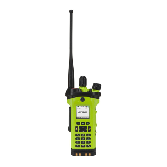
Motorola APX 5000 Service Manual
Hide thumbs
Also See for APX 5000:
- Service manual (318 pages) ,
- Quick reference card (2 pages) ,
- User manual (45 pages)

Related Manuals for Motorola APX 5000


Summary of Contents for Motorola APX 5000
- Page 1 APX™ TWO-WAY RADIOS APX 5000/ APX 6000/ APX 6000XE/ SRX 2200 Detailed Service Manuals...
- Page 3 ASTRO 5000/ APX 6000/ ® 6000XE/ SRX 2200 VHF/700–800 MHz/UHF1/UHF2 Digital Portable Radios Detailed Service Manual Motorola Solutions 1303 E. Algonquin Rd. Schaumburg, IL 60196-1078 U.S.A. 68012002028-C...
-
Page 4: Foreword
No duplication or distribution of this document or any portion thereof shall take place without the express written permission of Motorola. No part of this manual may be reproduced, distributed, or transmitted in any form or by any means, electronic or mechanical, for any purpose without the express written permission of Motorola. -
Page 5: Document History
The following major changes have been implemented in this manual since the previous edition: Edition Description Date 68012002028-A Initial edition Aug 2011 68012002028-B Added APX 5000 info Sept 2011 68012002028-C Added UHF2 info Jun 2012 Added UHF1: NUE7369A Added APX 6000XE and SRX 2200 info... - Page 6 Document History Notes...
-
Page 7: Table Of Contents
Table of Contents Table of Contents Foreword ......................ii Product Safety and RF Exposure Compliance ....................ii Manual Revisions ............................ii Computer Software Copyrights ........................ii Document Copyrights ..........................ii Disclaimer..............................ii Trademarks ..............................ii Document History ..................iii List of Tables ....................viii List of Figures ....................x Commercial Warranty ..................xv Limited Warranty ............................xv Chapter 1 Introduction ................. - Page 8 Table of Contents Power-Up Self-Check Errors......................4-4 Power-Up Self-Check Diagnostics and Repair (Not for Field Use)..........4-5 Chapter 5 Troubleshooting Charts ............. 5-1 List of Troubleshooting Charts ....................... 5-1 Main Troubleshooting Flowchart....................5-3 Power-Up Failure ........................... 5-4 DC Supply Failure........................5-15 Top/CID Display Failure.......................
- Page 9 Controller Board......................... 8-129 Expansion Board ........................8-157 Appendix A Replacement Parts Ordering..........A-1 Basic Ordering Information ......................A-1 Transceiver Board, VOCON Board and Expander Board Ordering Information......A-1 Motorola Online ..........................A-1 Mail Orders ............................A-1 Telephone Orders..........................A-1 Fax Orders.............................A-2 Parts Identification .........................A-2 Product Customer Service......................A-2 Glossary ..................
-
Page 10: List Of Tables
viii List of Tables List of Tables Table 2-1. Batteries ..........................2-1 Table 2-2. Transceiver Voltage Regulators .................... 2-3 Table 3-1. Battery Connector M101 ....................... 3-5 Table 3-2. VOCON Connector J1001 ....................3-5 Table 3-3. Port Expander Pin Settings ....................3-20 Table 3-4. - Page 11 APX 6000 Quick Reference Card Model 2................. PMLN5716_ APX 6000 Quick Reference Card Model 3................. PMLN5717_ APX 5000/ APX 6000/ APX 6000Li/ APX 6000XE Digital Portable Radios Basic Service Manual............................68012002028 APX 6000/ APX 7000 Digital Portable Radios User Guide (CD)..........PMLN5335_ APX 5000 Digital Portable Radios User Guide (CD)..............
-
Page 12: List Of Figures
List of Figures Figure 2-1. DC Power Distribution......................2-2 Figure 3-1. APX 5000/ APX 6000/ APX 6000XE/ SRX 2200 Overall Block Diagram......3-2 Figure 3-2. Transceiver (VHF) Block Diagram (Power and Control Omitted).......... 3-3 Figure 3-3. Transceiver (UHF1 and UHF2) Block Diagram (Power and Control Omitted) ...... 3-4 Figure 3-4. - Page 13 List of Figures Figure 3-50. Bluetooth Low-Frequency Circuit Block Diagram ............... 3-68 Figure 3-51. Bluetooth Low-Frequency Pairing Data Path..............3-68 Figure 3-52. Detailed Low-Frequency Transmit/Receive Paths .............. 3-69 Figure 3-53. Chip Power-Up/Power-Down Sequence (Exernal Input/Output Shown) ......3-69 Figure 3-54. Current Distribution Tree for Bluetooth Circuitry ..............3-70 Figure 3-55.
- Page 14 List of Figures Figure 6-45. F2_TIMER_OUT clock from CPLD into OMAP for eMMC operation ........6-47 Figure 6-46. Received Baseband Waveforms..................6-48 Figure 6-47. GPS TCXO Waveforms ...................... 6-49 Figure 6-48. GPS RTC Waveforms ......................6-50 Figure 6-49. GPS UART DATA Waveforms..................... 6-51 Figure 6-50.
- Page 15 List of Figures xiii Figure 8-26. NUE7365A Power Amplifier Circuit..................8-36 Figure 8-27. NUE7365A Transceiver (RF) Board Layout – Side 1 ............8-37 Figure 8-28. NUE7365A Transceiver (RF) Board Layout – Side 2 ............8-38 Figure 8-29. NUE7369A Receiver Front End Circuit................8-48 Figure 8-30.
- Page 16 List of Figures Figure 8-80. HLN5960A Controller Board Layout – Side 2 ..............8-151 Figure 8-81. HLN5978B Expansion Board Overall Circuit Schematic........... 8-157 Figure 8-82. HLN5977A/ HLN5978B Audio Circuit ................8-158 Figure 8-83. HLN5977A/ HLN5978B Secure Circuit ................8-159 Figure 8-84. HLN5978B Expandable Memory Circuit ................8-160 Figure 8-85.
-
Page 17: Commercial Warranty
Product Accessories One (1) Year Motorola, at its option, will at no charge either repair the Product (with new or reconditioned parts), replace it (with a new or reconditioned Product), or refund the purchase price of the Product during the warranty period provided it is returned in accordance with the terms of this warranty. Replaced parts or boards are warranted for the balance of the original applicable warranty period. - Page 18 Warranty service will be provided by Motorola through one of its authorized warranty service locations. If you first contact the company which sold you the Product, it can facilitate your obtaining warranty service. You can also call Motorola at 1-888-567-7347 US/Canada.
- Page 19 A. that MOTOROLA will be notified promptly in writing by such purchaser of any notice of such claim; B. that MOTOROLA will have sole control of the defense of such suit and all negotiations for its settlement or compromise; and C.
- Page 20 xviii Commercial Warranty Notes...
-
Page 21: Chapter 1 Introduction
This manual includes all the information needed to maintain peak product performance and maximum working time for the ASTRO APX 5000/ APX 6000/ APX 6000XE/ SRX 2200 radio. This detailed level of service (component level) is typical of the service performed by some service centers, self-maintained customers, and distributors. -
Page 22: Notations Used In This Manual
Introduction: Notations Used in This Manual Notations Used in This Manual Throughout the text in this publication, you will notice the use of warnings, cautions, and notes. These notations are used to emphasize that safety hazards exist, and care must be taken and observed. -
Page 23: Chapter 2 Radio Power
APX 6000/ APX 6000XE/ SRX 2200 radio. General In the ASTRO APX 5000/ APX 6000/ APX 6000XE/ SRX 2200 radio, power (B+) is distributed to two boards: the transceiver (RF) board and the VOCON board (see Figure 2-1 on page 2-2). -
Page 24: Dc Power Routing - Transceiver Board
Radio Power: DC Power Routing – Transceiver Board Battery RF Board VOCON Board PMOS M101 BATT SW_B+ Switch Fuse 3.6Vdc External P101 5.4Vdc External SW 1.4Vdc RAW B+ External SW 5Vdc 1.85Vdc 1.85Vdc 2.23Vdc External 5Vdc External LDO 3Vdc 3.6Vdc MAKO 3Vdc 1.8 Volts... -
Page 25: Dc Power Routing - Vocon Board
Radio Power: DC Power Routing – VOCON Board The transceiver regulated power supplies are summarized in Table 2-2. Table 2-2. Transceiver Voltage Regulators Reference Output Description Designator Name Signal Name U200 LP2989 DC_LIN_5V Regulated 5.0 Vdc U201 LP5900 DC_LIN_3V Regulated 3.0 Vdc U202 LP5900 DC_LIN_1_8V... - Page 26 Radio Power: DC Power Routing – VOCON Board Notes...
-
Page 27: Chapter 3 Theory Of Operation
This detailed theory of operation can help isolate the problem to a particular component. The ASTRO APX 5000/ APX 6000/ APX 6000XE radio, which is a single-band synthesized radio, is available in the VHF (136–174 MHz), 7/800 (764–870 MHz), UHF1 (380–470 MHz) and UHF2 (450–520 MHz) frequency bands. -
Page 28: Figure 3-1. Apx 5000/ Apx 6000/ Apx 6000Xe/ Srx 2200 Overall Block Diagram
Theory of Operation: Bluetooth Antenna Antenna Expansion External Accessory Connector Board External Antenna Front Display Transceiver Keypad Board VOCON Board Top Display Controls Top Figure 3-1. APX 5000/ APX 6000/ APX 6000XE/ SRX 2200 Overall Block Diagram... -
Page 29: Transceiver Board
Theory of Operation: Transceiver Board Transceiver Board The transceiver (XCVR) board performs the transmitter and receiver functions necessary to translate between voice and data from the VOCON board and the modulated radio-frequency (RF) carrier at the antenna. The transceiver board contains all the radio’s RF circuits for the following major components: •... -
Page 30: Figure 3-3. Transceiver (Uhf1 And Uhf2) Block Diagram (Power And Control Omitted)
Theory of Operation: Transceiver Board Transmitter Receiver Indicates Sub-shield SP3T Rf Switch Digital RF Atten SP3T Driver SP2T Amplifier Harmonic Filter Atten coupler Power Detector LOOP UHF TX FILTER 16.8MHz BUFFER TRIDENT IC TX LO UHF RX LOGIC PRESCALAR BUFFER EXPANDER BUFFER 16.8MHz... -
Page 31: Table 3-1. Battery Connector M101
Theory of Operation: Transceiver Board 3.1.1 Interconnections This section describes the various interconnections for the transceiver board. 3.1.1.1 Battery Connector M101 Battery connector M101 solders to the transceiver printed circuit board. The connector has 5 gold plated contacts that mate with the battery, two contacts for positive, two for negative and one for the Dig_Battery_Data. - Page 32 Theory of Operation: Transceiver Board Table 3-2. VOCON Connector J1001 (Continued) XCVR VOCON Signal XCVR Signal Type Description TX_INH DIG_CTRL_TX_INHIBIT_TYPE_1 control TX inhibit control for secure RX_DA DIG _DATA _SSI _RX _DOUTA RX SSI data RF_DAC_SPI_CS DIG_CTRL_SPI_DAC_PE SPI DAC chip select RX_CLK CLK_SSI_RX RX SSI clock...
-
Page 33: Figure 3-5. Receiver Block Diagram (Vhf)
Theory of Operation: Transceiver Board 3.1.1.3 Antenna Port J101 Antenna port J101 is a surface-mount, miniature coaxial connector for the antenna cable. 3.1.1.4 Serial EEPROM The electrically erasable programmable memory (EEPROM), U101, holds all of the transceiver tuning data. This allows transceivers to be tuned in the factory and installed in the field without retuning. -
Page 34: Figure 3-6. Receiver Block Diagram (Uhf1 And Uhf2)
Theory of Operation: Transceiver Board DPLXR SP3T ΣΔ Dec. Filter RF/Vocon Connector 18Mhz Abacus III Figure 3-6. Receiver Block Diagram (UHF1 and UHF2) DPLXR SP3T 700/800 ΣΔ Dec. Filter RF/Vocon Connector 18Mhz Abacus III Figure 3-7. Receiver Block Diagram (7/800) - Page 35 Theory of Operation: Transceiver Board 3.1.2.1 VHF Front-End From the attenuator, U1149, a VHF signal is routed to the first pre-selector filter followed by a Low Noise Amplifier (LNA) and a second pre-selector filter. Both filters are discrete and fixed designs and are used to band limit the incoming energy and suppress known spurious responses such as Image and the ½...
- Page 36 The UHF1 SRX 2200 is available with a low power setting that limits the transmit power to 0.25 watt. The rest of the APX 5000/ APX 6000 radios and the SRX 2200 VHF radio are able to be limited to...
-
Page 37: Figure 3-8. Transmitter Block Diagram (Vhf)
Theory of Operation: Transceiver Board 3-11 Log Amp Power Detector SP3T RF Switch Digital RF Attenuator Transmitter FET VHF TX Buffer Amp Antenna Connector Directional TX Driver Amplifier Harmonic LP Filter Coupler To RX Reverse Power Detection Loop Filter TX VCO Ref. -
Page 38: Figure 3-10. Transmitter Block Diagram (7/800)
3-12 Theory of Operation: Transceiver Board Log Amp Power Detector SP3T RF Switch Digital RF Attenuator Transmitter FET 7/800 TX Buffer Amp SP2T To Antenna To RMT Port Directional TX Driver Amplifier Harmonic LP Filter Coupler To RX Reverse Power Detection Loop Filter TX VCO Ref. -
Page 39: Directional Coupler
Theory of Operation: Transceiver Board 3-13 3.1.3.1 Driver Amplifier The driver amplifier IC (VHF – U902, UHF1 – U1602, UHF2 – U1500 and 7/800 – U1002) contains one LDMOS FET amplifier stages and an internal resistor bias networks. Pin 16 is the RF input. Modulated RF from the FGU, at a level of +3 dBm ±2 dB, is coupled through a blocking capacitor to the gate of FET-1. -
Page 40: Harmonic Filter
3-14 Theory of Operation: Transceiver Board 3.1.3.4 Harmonic Filter The harmonic filter is a high-power, low-loss, low-pass filter. Its purpose is to suppress transmitter harmonics. The filter also improves receiver out-of-band rejection. The appropriate shield over the filter must be in place to achieve the required stop band rejection. VHF: The harmonic filter uses discrete components. - Page 41 Theory of Operation: Transceiver Board 3-15 3.1.3.7.1 Voltage Control Mode The heart of the voltage control loop is a logarithmic amplifier based power control IC, U1105. Quad DAC, U1125, receives the power tuning values via the SPI bus and converts them into a voltage at “VOUTB.”...
- Page 42 3-16 Theory of Operation: Transceiver Board 3.1.3.7.3 Current Control Mode In TDMA mode, excessive transient adjacent channel splatter caused by the RFPA, when it is under a greater degree of compression than is expected at nominal supply voltage, is mitigated through a system of saturation detection and switching of the TX power control mode from the voltage control loop to the current control loop.
-
Page 43: Figure 3-11. Synthesizer Block Diagram (Vhf)
Theory of Operation: Transceiver Board 3-17 VHF DIVIDE-BY-2 HARMONIC FILTER 16.8MHz BUFFER BUFFER 16.8MHz LOOP FILTER TX LO VHF TX TRIDENT IC RX LO BUFFER VHF RX LOGIC EXPANDER PRESCALAR BUFFER Figure 3-11. Synthesizer Block Diagram (VHF) 16.8MHz BUFFER BUFFER 16.8MHz LOOP FILTER... -
Page 44: Figure 3-13. Synthesizer Block Diagram (7/800)
Components L753 and C754 form a low-pass filter to reduce the harmonics of the 16.8 MHz. 3.1.4.2 Trident IC U702 The Trident IC, U702, is a multiple protocol, multiple band transceiver Motorola-proprietary, CMOS IC, with built-in dual-port modulation. The Trident IC incorporates frequency division and comparison circuitry to keep the VCO signals stable. - Page 45 3-19 3.1.4.5 Modulation To support many voice, data, and signaling protocols, APX 5000/APX 6000/APX 6000XE/SRX 2200 radios must modulate the transmitter carrier frequency over a wide audio frequency range, from less than 10 Hz up to more than 6 kHz. The Trident IC supports audio frequencies down to zero Hz by using dual-port modulation.
-
Page 46: Table 3-3. Port Expander Pin Settings
3-20 Theory of Operation: Transceiver Board 3.1.4.8 Port Expander U703 is a port expander that is controlled by the auxiliary SPI of the Trident IC; pins A7 (ASPI_DATA), B7 (ASPI_CLK) and C6 (ACE1_GPO7). Data sent on the main SPI bus with a specific header, tells the Trident IC to pass the data (via the auxiliary SPI lines) onto the port expander SPI lines, pins 32 (SCLK), 33 (DIN) and 34 (CS). - Page 47 Theory of Operation: Transceiver Board 3-21 Table 3-3. Port Expander Pin Settings (Continued) PIN NO. UHF R1 TX LOGIC (380–445) PIN NO. LOGIC PIN NO. UHF R1 TX LOGIC (445–470) PIN NO. LOGIC PIN NO. UHF R1 RX LOGIC (380–449.65) PIN NO.
- Page 48 3-22 Theory of Operation: Transceiver Board 3.1.4.9 Buffers and VCOs Q774 and surrounding circuitry is the prescalar buffer that takes the output of the VCOs and feeds the prescalar input to the Trident IC, pin G1 (M_PRSC). Q713 and surrounding circuitry is a buffer that provides the correct drive level to the receiver section (via the transmission line TL_RX_LO) and to the input to the TX buffer (Q842 and surrounding circuitry).
- Page 49 Theory of Operation: Transceiver Board 3-23 UHF2: The TX and RX VCOs used for UHF2 are contained in Y705 and Y704. To select UHF RX VCO (450–520 MHz), pin 3 (SEL1) must be at a low logic level and pin 5 (SEL 2) at a high logic level, on Y704.
-
Page 50: Controller
: Controller Controller 3.2.1 Controller Overview This section provides a detailed circuit description of the APX 5000/APX 6000/APX 6000XE/ SRX 2000 controller design. The controller design consists of the following board and flexes: Printed Circuit Boards • VOCON Board • Expansion Board •... - Page 51 Theory of Operation : Controller 3-25 3.2.1.1 Main Controller Components and Connections 3.2.1.1.1 VOCON Board The VOCON Board contains the OMAP1710 dual-core processor, FLASH and SDRAM memory, Audio circuitry (MAKO and CODEC IC's), a Complex Programmable Logic Device (CPLD), and interfaces to the other components in the controller design.
-
Page 52: Figure 3-15. Controller Electrical Overview
Theory of Operation 3-26 : Controller 3.2.1.2.4 Data-Side Microphone The data-side microphone is mounted on the front chassis and connects directly to the VOCON board through a set of pogo pins mounted on the VOCON board. 3.2.1.2.5 Side Controls Flex The side controls flex contains the PTT, Side Top button, Side Middle button and Side Bottom button. -
Page 53: Figure 3-16. Controller Dc Block Diagram
Theory of Operation : Controller 3-27 The functional blocks of the controller are: • DC Distribution • Clock Sources • Processor / Memory • e-MMC Expandable Memory (expansion board) • CPLD • Audio – Internal and External • MAKO • User Interfaces •... -
Page 54: Table 3-4. Dc Supplies And Sources For Controller
Theory of Operation 3-28 : Controller Table 3-4. DC Supplies and Sources for Controller OMAP CORE OMAP IO FLASH CPLD MACE CODEC LGHT FRNT LGHT TOP RF BOARD MAKO CLASS D PA TOP DSPLY FRNT DSPLY USB SPLY 16.8 SQR... -
Page 55: Table 3-5. Mako's Ldo And Supplies
Theory of Operation : Controller 3-29 3.2.2.1 DC Distribution Major Components The controller's DC section is made up of MAKO and external regulators. This section will give an overview of the schematics and circuitry that makes up the major supplies of the DC architecture. 3.2.2.1.1 MAKO MAKO (U6501) is a custom power management IC manufactured by Atmel. -
Page 56: Figure 3-17. V_Sw_1.4 Switched Power Supply
Theory of Operation 3-30 : Controller 3.2.2.1.2 External Regulators: V_SW_1.4, V_SW_3.60 The controller board contains two TPS62050 regulators in order to regulate voltages of 1.4V and 3.6V. The TPS62050 is a synchronous step-down adjustable regulator. The switching regulator is capable of sourcing 800mA. Its output can be adjusted by using a voltage divider tied to the feedback pin. -
Page 57: Table 3-6. Pulse Switching Combination
PA_SHTDN 5V_PWM_EN Figure 3-18. 5V Switched Power Supply APX 5000/APX 6000/APX 6000XE/SRX 2200 has Pulse Switching option. Mode 1: Pulse Frequency Modulation (PFM). A relatively noisy but highly efficient pulsing mode for Switched power supplies. Mode 2: Pulse Width Modulation (PWM). Pulsing mode that is cleaner than PFM, used when risk of RF interference is present which includes both transmit and receive radio modes. -
Page 58: Figure 3-19. Power-Up Timing Regulators
Theory of Operation 3-32 : Controller 3.2.2.1.4 Power-up Timing The powering up of the radio starts with the MAKO. Once the radio knob is turned to the 'ON' position and battery voltage is supplied, a pass FET is activated to deliver battery voltage to MAKO and external regulators. -
Page 59: Table 3-7. Vocon Clock Distribution
Theory of Operation : Controller 3-33 3.2.3 Clock Sources The VOCON board contains multiple crystal clock sources. These sources are active upon power- up. Secondary clock frequencies are derived on the VOCON board from these crystal sources. In addition to the crystal frequencies, the VOCON receives a 16.8 MHz sine wave from the RF board, which is shaped into square wave and fed to the OMAP timer input. -
Page 60: Figure 3-21. Overview Of Omap Interconnection With Vocon Peripherals
Theory of Operation 3-34 : Controller 3.2.4 OMAP Processor and Memory 3.2.4.1 OMAP Processor (U6302) The OMAP1710 dual core processor lies at the center of the VOCON design. The processor features utilized in the VOCON design include: • ARM9 CPU core •... -
Page 61: Figure 3-22. Omap Memory Interface
Theory of Operation : Controller 3-35 3.2.4.2 Memory In addition to the internal RAM, the OMAP 1710 Processor (U6302) features three distinct external memory interfaces. All memory devices except the eMMC memory, is located on the VOCON board, as elaborated in Figure 3-21. - Page 62 Theory of Operation 3-36 : Controller 3.2.4.6 Synchronous External Memory Interface This interfaces the OMAP to a 32 MB Double Data Rate (DDR) RAM IC (U6301). Upon boot-up OMAP configures this interface to operate in synchronous mode at 96MHz. This volatile memory unit is primarily accessed during code execution.
-
Page 63: Figure 3-23. Timing Of Power-Up And Initialization Of Emmc
Theory of Operation : Controller 3-37 A GPIO named "MMC_RESET" will be used to soft-reset the eMMC card. This will be an output from CPLD ball C7. This ball is on output high out of reset. On power-up software should drive the pin low for at least 5ms and then drive it high. -
Page 64: Figure 3-24. Emmc Topography
Theory of Operation 3-38 : Controller e·MMC controller RST_n Registers DAT[7:0] ECSD * internally connected. NAND Flash Symbol Type Description Input Clock: Each cycle of the clock directs a transfer on the command line and on the data line(s). The frequency can vary between the minimum and the maximum clock frequency. Command: This signal is a bidirectional command channel used for command and response transfers. -
Page 65: Figure 3-25. Block Diagram Of Vocon And Expansion Boards As Related To Emmc
Theory of Operation : Controller 3-39 VOCON Board Expansion Board V_SW_3.6 V_EXT_1.85v U6508 MAKO U6501 VCC_1.85v V4_2775D V_2.775_EXP jumper R6562 VCC_2.775 eMMC CPLD U6101 MMC_CMD MMC_CLK Voltage EMMC_RESET translator F2_Timer_out U2415 MMC_DAT0 MMC_DAT1 AVR_STATUS_3.3 MMC_DAT2 MMC_DAT3 OMAP 1710 U6302 AVR_STATUS_1.8 Figure 3-25. -
Page 66: Figure 3-26. Rx / Tx Ssi Configuration
Theory of Operation 3-40 : Controller 3.2.4.10 Peripheral Devices The OMAP processor is equipped with multiple buses and interfaces that are configured for peripheral interconnection. 3.2.4.10.1 Receive and Transmit SSI These two interfaces are dedicated for communicating with the RF deck digital interface, carrying receive and transmit base band signals. -
Page 67: Figure 3-28. Spi And I2C Configuration
Theory of Operation : Controller 3-41 3.2.4.10.3 ARM SPI This SPI interface is controlled by OMAP's ARM core. Devices connected to this bus include MAKO, display controllers and the audio CODEC. 3.2.4.10.4 DSP SPI This SPI interface is controlled by the DSP core of the OMAP processor. This bus is used to configure and control devices on the RF deck. -
Page 68: Figure 3-29. Cpld Block Diagram
Theory of Operation 3-42 : Controller 3.2.4.10.7 UARTs Two of OMAP's UARTs are configured for peripheral interfacing. The four-wire UART1, which is capable of hardware flow control, is available on the side connector for accessory devices. The signals are level translated via MAKO and routed to the side connector via J4001. -
Page 69: Figure 3-30. Audio Tx Path Block Diagram
Theory of Operation : Controller 3-43 3.2.5 Audio The audio section of the VOCON design consists of: • TI AIC33 voice CODEC • TI TPA2034D1 class-D audio power amplifier • MAKO audio sub-block 3.2.5.1 TX Audio path The TX audio paths begin with three microphones. There are two internal microphones and one external microphone path going to the GCAI connector. -
Page 70: Figure 3-31. Vocon Rx Audio Path Block Diagram
Theory of Operation 3-44 : Controller 3.2.5.2 RX Audio path The RX audio path supports two internal speakers and one external speaker. OMAP DSP MAKO AB AMP External/ Accessory Speaker MCBSP1 ~ 16-20 Ohms Switch AB AMP ARM SPI Low-Pass Filter 20kHz Corner Class D TPA2034D1... -
Page 71: Figure 3-32. Control Top Block Diagram
Theory of Operation : Controller 3-45 3.2.6 User Interface 3.2.6.1 Control Top The control top contains an On/Off & Volume Knob (S3), a sixteen-position Channel/Frequency Switch with programmable concentric two-position switch (S2), a three-position (A,B,C) Programmable Toggle Switch (S4), and an orange programmable Top Button (S1). The Control Top also includes a TX/RX LED that is solid amber upon receive, red on PTT, and blinks amber on secure RX. -
Page 72: Figure 3-33. Display Circuit Detail Overview Block Diagram
3.2.6.2 APX 5000/ APX 6000/ APX 6000XE/ SRX 2200 LCD Display Modules 3.2.6.2.1 QVGA The APX 5000/APX 6000/APX 6000XE/SRX 2200 radio can have up to 2 displays (QVGA and FSTN) depending upon the particular feature set and radio model ordered. The main Transflective 1.6"... - Page 73 3.2.6.2.2 FSTN All APX 5000/APX 6000/APX 6000XE/SRX 2200 Radios are equipped with a caller ID (CID) top display. This top display is a 1.1", Transflective, FSTN (Film compensated Super Twisted Nematic) 32 row x 112 column LCD with black pixels on a light background. This display is a component of the control top sub-assembly with all interconnections passing through control top FPC.
-
Page 74: Table 3-8. Color Schemes
: Controller 3.2.6.3 Intelligent Lighting The APX 5000/APX 6000/APX 6000XE/SRX 2200 radio is equipped with numerous LEDs to provide intelligent lighting features. The VOCON board contains 2 lighting controller devices, which illuminate all the LEDs throughout the radio, as shown in Figure 3-34. -
Page 75: Figure 3-34. Lighting Controller Overview
Theory of Operation : Controller 3-49 3.2.6.3.2 Secondary Lighting Controller As previously mentioned the secondary lighting controller provides illumination to the top display backlight and Tx/Rx indicator lamp. The lighting controller and LEDs are powered by switcher 5 (V_SW_5). This lighting controller device uses a PWM output to control the dimming modes of operation for each LED. -
Page 76: Figure 3-35. Lighting Controller - Srx 2200
Theory of Operation 3-50 : Controller 3.2.6.3.3 Secondary Lighting Controller – SRX 2200 Figure 3-35 shows the major connection scheme to this secondary lighting controller exclusively for SRX 2200. A lighting system has been put into place to accommodate night profiles. These profiles shift both displays and the keypad to a lower brightness. -
Page 77: Table 3-9. Key Map Matrix
Theory of Operation : Controller 3-51 3.2.6.4 Keypad The Dual Display Model contains a 21 button keypad, which translates to a 5x5 row and column keypad matrix as shown in Figure 3-36. The keypad also contains LEDs for the backlighting of the keys, which is described in more detail in Section 3.2.6.3: "Intelligent Lighting". -
Page 78: Side Controls
Theory of Operation 3-52 : Controller Table 3-9. Key Map Matrix (Continued) Row, Column Map Row, Column Map 2 , 3 0 , 1 3 , 0 0 , 2 3 , 1 3.2.6.5 Side Controls The side controls include three programmable, momentary, pushbutton switches (Side Button 1 [SB1], Side Button 2 [SB2], Top Side Button [MON]) and a Push-To-Talk switch [PTT]. -
Page 79: Figure 3-37. Gcai Signal Configuration
Theory of Operation : Controller 3-53 GCAI CONNECTOR OMAP1710 MA KO ONE_WIRE_GCAI ONE_WIRE One-Wire BATT_STATUS GPIO_0 One-Wire VBUS Vbus TXEN PORT 0 XCVR UART1_RX SPKR+ UART1_RX UART1_TX SPKR- UART1_TX GPIO_3 MIC+ Ext Mic MIC- Preamp KF Switch OPTA_SEL_2 GPIO_4 GPIO OPT_GPIO_3 GPIO OPTA_SEL_1... -
Page 80: Table 3-11. Gcai Connector Pin Assignment
Theory of Operation 3-54 : Controller Table 3-10. P1 Pin Assignment P1 PIN ASSIGNMENT SIDE CONNECTOR SIGNAL GCAI_VBUS_5V GCAI_VBUS_5V GCAI_USB_P_GPIO1 / TxDc / FillReq GCAI_USB_N_GPIO2 / RxDc / FillData GCAI_GPIO0 / PwrOn GCAI_CTS_GPIO_4 / KeyFail / FillClk GCAI_MIC_P GCAI_MIC_N GCAI_SPKR_N / LineOut- GCAI_SPKR_P / LineOut+ GCAI_RTS_GPIO_3 / OTG-ID / FillSen GCAI_ONE_WIRE... -
Page 81: Figure 3-39. Gcai Connector - Back View
Theory of Operation : Controller 3-55 Table 3-11. GCAI Connector Pin Assignment (Continued) PIN ASSIGNMENT SIGNAL GCAI_MIC_N GCAI_CTS_GPIO_4 / KeyFail / FillClk Figure 3-39. GCAI Connector – Back View... -
Page 82: Figure 3-40. Vocon To Rf Board Interface
Theory of Operation 3-56 : Controller 3.2.7 RF Interface The VOCON to RF board interface through connector J1001. See Figure 3-40. RF - VoCon Interface 33,31,29 N14,P14,AA17 McBSP3 ABCS GPIO59 GPIO17 TRCS EEPROM_CS GPIO28 DAC_CS GPIO61/SPIF_CS2 LOCK GPIO56 19,17,21 Y6,W7,AA5 McBSP2 TX SSI OMAP... -
Page 83: Figure 3-41. Apx 5000/ Apx 6000/ Apx 6000Xe/ Srx 2200 Encryption Architecture
J4001-P2001 connector. The encryption circuitry is designed to digitally encrypt and decrypt voice and ASTRO data in the APX 5000/APX 6000/APX 6000XE/SRX 2200 radio. The Motorola Advanced Crypto Engine (MACE) IC is the main component in the encryption design, and has some discrete support circuitry along with the interfaces to the VOCON IC's (CPLD, OMAP, and Audio CODEC). -
Page 84: Table 3-12. Encryption Algorithms And Corresponding Kit Numbers
ERROR 09/10 message on the display. Table below lists the encryption algorithms and their corresponding kit numbers. Table 3-12. Encryption Algorithms and Corresponding Kit Numbers KIT Number Description APX 5000/APX 6000/APX 6000XE/SRX 2200 NNTN8171_ DVP-XL KIT APX 5000/APX 6000/APX 6000XE/SRX 2200 NNTN8172_... - Page 85 Theory of Operation : Controller 3-59 3.2.8.3 Key Retention The key variables are retained within the MACE IC's memory (SRAM or FLASH). The keys can be infinite key retention or 30-seconds key retention, depending on how the codeplug is set up. When set to infinite key retention, the keys are stored in the FLASH memory inside the MACE IC.
-
Page 86: Global Positioning Sytem (Gps)
Theory of Operation 3-60 : Global Positioning Sytem (GPS) Global Positioning Sytem (GPS) The APX 6000/APX 6000XE/SRX 2200 GPS architecture employs the Texas Instruments NL5500 GPS IC (U2401) which decodes GPS signals at 1575.42 MHz (L1 band). It is capable of producing a final position solution including full tracking and data decode capability. -
Page 87: Table 3-13. Power And I/O Pins For Ni5500
Theory of Operation : Global Positioning Sytem (GPS) 3-61 Table 3-13. Power and I/O Pins for NI5500 Signal Name Type NL5500 ball(s) Source/Destination [ref] Description (board VBAT Power A2, H1, D8 VSW_3.6 [U6504] (Vocon) Main NL5500 power supply VDDS Power B3, G10, K5, E2 VCC_1.85 [U6508] (Vocon) I/O Power Supply... -
Page 88: Accelerometer
Theory of Operation 3-62 : Accelerometer RF-VOCON-Exp Interconnect RF Board Expansion Board External Regulators 3.6V 1.8V 2.8V (VSW_3.6) (VCC_1.85) VBAT VDDS VDD_TCXO (G1) LNA Enable TCXO GPS_EXT_LNA_EN (H6) TCXO_CLK_LV (F1) 3.0V 26MHz, <0.5ppm GPS IC GPS_LNA_IN (L2) [OMAP 1710] TI NL5500 GPS Tx GPS_UART_TX (F5) UART2 Rx (R9) -
Page 89: Table 3-14. Spi Interface
Theory of Operation : Accelerometer 3-63 3.3V LDO Core Voltage Accelerometer Data Bus Accelerometer LIS331DLH AT32UC3A (Bus Slave) (Bus Master) Interrupts Figure 3-45. Accelerometer Block Diagram The registers embedded on the LIS331DL are accessed through SPI serial interface. The following pins are responsible for the SPI communication. -
Page 90: Table 3-15. Register Address Map
Theory of Operation 3-64 : Accelerometer The following table provides a list of the registers and their respective addresses used for the accelerometer IC (LIS331DL). Table 3-15. Register Address Map Name Type Register Address Default Comment Binary Reserved (do not modify) 00 –... -
Page 91: Bluetooth
Low-frequency transmission is done by the host controller itself using a NOR gate. The Bluetooth antenna is made of a flexible PCB and is a modified PIFA with a 2.5 dBi gain. The Bluetooth antenna is mounted in the APX 5000/APX 6000/APX 6000XE/SRX 2200 speaker assembly: Speaker Assembly... -
Page 92: Figure 3-47. Bluetooth Connection Flowchart
Theory of Operation 3-66 : Bluetooth To connect a Bluetooth accessory, the blue pairing indicators on the accessory and the radio should be brought close to each other with the Bluetooth feature enabled and on in the radio. The LF/Bluetooth connection flow is shown in Figure 3-47. -
Page 93: Figure 3-48. Bluetooth/Controller Interface With Clock Sources
SPI0 USART1 UART BLOCK TIMER1 TX_CLK GPIO WAKEUP ATMEL AVR32 BT_PTT AT32UC3A0512 ANTENNA OMAP_GPIO7 GPIO USART1 TX APX 5000/ APX 6000/ TC1 OCA APX 6000XE/ SRX2200 Expansion Board USART0 GPIO GPIO Antenna 80-PIN CONNECTOR Antenna BT_HCI BT_WAKE BT_EN PCM_AUD BT_RF 2.45 GHz BPF... -
Page 94: Figure 3-50. Bluetooth Low-Frequency Circuit Block Diagram
Theory of Operation 3-68 : Bluetooth To verify the Bluetooth transmitter is operational, an RCMP command can be sent to transmit a constant carrier waveform on a Bluetooth frequency. To verify the LF transmit feature is operational, an RCMP command can be sent to transmit a constant carrier waveform at 125 kHz. There are similar RCMP commands for verifying BT/LF RSSI when a CW BT/LF signal is applied near the antennas of the BT/LF circuitry. -
Page 95: Figure 3-52. Detailed Low-Frequency Transmit/Receive Paths
Bluetooth IC core and a 1.85V (U6508, VDDS) supply for the I/O. It has a shutdown (U2415 pin L3) that must be high for operation to work. The power-up/down sequence required for operation is shown in Figure 3-53. APX 5000/ APX 6000/ APX 6000XE/ SRX2200 7.5V Batt Partial Current Tree VDDS <2.5ms... -
Page 96: Figure 3-54. Current Distribution Tree For Bluetooth Circuitry
Theory of Operation 3-70 : Bluetooth The host processor operates from a 3.3V LDO regulator (U2402). The 1.85V regulator enables the 3.3V LDO regulator output. The LF receiver IC is powered from a 3.3V LDO regulator (U2402). Figure 3-54 is a partial current tree showing the flow of current from the battery to the Bluetooth- related major components sourced by the 3.6V switching regulator on the VOCON. -
Page 97: Table 3-16. Bluetooth Host Processor Uart I/O
Theory of Operation : Bluetooth 3-71 3.5.3 Bluetooth I/Os. The communication between the Bluetooth IC and the host controller is by a four-wire HCI USART0 bus (RX, TX, CTS, RTS). The Bluetooth IC receives a firmware update over USART0 each time it is powered on. -
Page 98: Table 3-17. Spi I/O
Theory of Operation 3-72 : Bluetooth The Bluetooth IC shutdown (U2415 pin L3) and wakeup (U2415 pin K3) pins are also connected to the host controller. A Bluetooth PTT pin on the host controller (U2415 pin J2) tells the OMAP (U6302 pin Y5) when the user pressed the PTT button on the Bluetooth accessory. -
Page 99: Table 3-19. Gpio I/O
The ATMEL bootloader is being used as a first stage bootloader that will jump to the Motorola bootloader, which is a stage two bootloader. GPIO20 is used by the ATMEL bootloader to trap in Flash mode. GPIO19 will be used by the Motorola bootloader to trap in Flash mode. Both pins are active low. - Page 100 Theory of Operation 3-74 : Bluetooth Notes...
-
Page 101: Chapter 4 Troubleshooting Procedures
The purpose of this chapter is to aid in troubleshooting problems with the ASTRO APX 5000/APX 6000/APX 6000XE/SRX2200 radio. It is intended to be detailed enough to localize the malfunctioning circuit and isolate the defective component. It also contains a listing of service tools recommended for PC board repair at the component level. -
Page 102: Recommended Service Tools
PC board repairs at the component level. For listings of additional service tools, service aids, and test equipment that are recommended for all levels of service, refer to the APX 5000/APX 6000/APX 6000XE/SRX2200 basic service manual (see “Related Publications”... -
Page 103: Standard Bias Table
Troubleshooting Procedures: Standard Bias Table Standard Bias Table Table 4-2 outlines some standard supply voltages and system clocks which should be present under normal operation. These should be checked as a first step to any troubleshooting procedure. Table 4-2. Standard Operating Bias – DC Voltages Name Reference Description... -
Page 104: Power-Up Self-Check Errors
Troubleshooting Procedures: Power-Up Self-Check Errors Power-Up Self-Check Errors Each time the radio is turned on, the MCU and DSP perform a series of internal diagnostics. These diagnostics consist of checking such programmable devices as the FLASH ROMs, the EEPROM, and SRAM devices. Problems detected during the power-up self-check routines are presented as error codes on the radio’s display. -
Page 105: Power-Up Self-Check Diagnostics And Repair (Not For Field Use)
Troubleshooting Procedures: Power-Up Self-Check Diagnostics and Repair (Not for Field Use) Power-Up Self-Check Diagnostics and Repair (Not for Field Use) Table 4-5 lists additional action items that can be used for the diagnosis and resolution of the error codes listed in Table 4-4 on page 4-4. - Page 106 Troubleshooting Procedures: Power-Up Self-Check Diagnostics and Repair (Not for Field Use) Table 4-5. Power-Up Self-Check Diagnostic Actions (Continued) Error Code/ Error Diagnostic Actions Message Hardware board Expansion board does not support bluetooth feature. Send radio to depot. mismatch If the Expansion board type supports “Full feature” – “Mace/GPS/BT/SDMem Exp Board”, updating the expansion board firmware should resolve the error message.
-
Page 107: Chapter 5 Troubleshooting Charts
Chapter 5 Troubleshooting Charts This section contains detailed troubleshooting flowcharts. These charts should be used as a guide in determining the problem areas. They are not a substitute for knowledge of circuit operation and astute troubleshooting techniques. It is advisable to refer to the related detailed circuit descriptions in the theory of operation sections prior to troubleshooting a radio. - Page 108 Troubleshooting Charts: List of Troubleshooting Charts Table 5-1. Troubleshooting Charts (Continued) Page Troubleshooting eMMC Memory Failure 5-34 RX RF RX RF Failure 5-35 FGU Failure 5-46 FGU Power Failure 5-47 GPS Failure 5-48 Bluetooth Failure Pairing Issue 5-49 LCD Indication 5-52 No Audio from Headset 5-54...
-
Page 109: Main Troubleshooting Flowchart
Troubleshooting Charts: Main Troubleshooting Flowchart Main Troubleshooting Flowchart Start Go to either Display Good Any Error Failure(5.19,5.20) power up Message? or Vocon power up self test failure flowchart Chart 5.3 See Button Test See Table for Buttons error codes Flowchart(chart Functional? Table 4.5 5.10) - Page 110 Troubleshooting Charts: Power-Up Failure Power-Up Failure – VOCON Board Name Description Level V Flow Chart VOCON Board Power Up VCC_1.875 C4001 LDO Output 1.875±10% Refer to note 1 Problem VCC_1.55 R6561 LDO Output 1.55±10% Low LDO3 VCC_1.55 Voltage VCC_2.775D R4011 LDO Output 2.775±10% Low LDO10 VCC_3.3 Voltage...
-
Page 111: Power-Up Failure
Troubleshooting Charts: Power-Up Failure Power-Up Failure – B+ Incorrect Voltage B+ Incorrect Voltage Check Voltage at Test Point F_UNSW_B+ (VOCON) Check Mating RF to Vocon Replace 6 < V < 9? Connector to RF Connectors Connector Board Replace RF Board, Check Replace VOCON 6 <... - Page 112 Troubleshooting Charts: Power-Up Failure Power-Up Failure – Low LDO10 VCC_3.3 Voltage Synopsis Low LDO10 VCC_3.3 Voltage This failure specifically refers to LDO10 but this flow chart can be used to diagnose LDO9, lDO7, and LDO6. All LDOs mentioned above are fed from the same source and have very limited differences.
- Page 113 Troubleshooting Charts: Power-Up Failure Power-Up Failure – Low LDO3 V_1.55 Voltage Low LDO3 V_1.55 Synopsis Voltage This failure specifically refers to LDO3 but this flow chart can be used to diagnose LDO2. All LDOs mentioned above are fed from the same source and have very limited differences.
- Page 114 Troubleshooting Charts: Power-Up Failure Power-Up Failure – Low LDO8 V_5.0A Voltage Low LDO8 V_5.0A Voltage Measure Radio Current Is Standby Current more Board has a short, than 15mA above Replace VOCON Average Inspect R6565 Connection Is R6565 Correct R6565 Soldered Soldering Properly Measure Voltage...
- Page 115 Troubleshooting Charts: Power-Up Failure Power-Up Failure – Low VBUS2 Voltage Low VBUS2 Voltage Measure V_SW_5 at C6567 Proceed to Low 5.1 < V < 5.6? SW5 Volatge Flow Chart Measure VBUS1 Supply Volatge at R6529 Inspect U6503 and Supporting Ciruitry Are Parts Solder Check Placement Is Part Placed...
- Page 116 5-10 Troubleshooting Charts: Power-Up Failure Power-Up Failure – Low V_SW_1.4 Voltage Low V_SW_1.4 Voltage Measure Radio Current Is Standby Current more Board has a short, than 15mA above Replace VOCON Average Measure SW_B+ Voltage at C6593 Proceed to 6 < V < 9? Incorrect B+ Voltage Measure Voltage...
- Page 117 Troubleshooting Charts: Power-Up Failure 5-11 Power-Up Failure – Low V_2.23 Voltage Low V_2.23 Voltage Measure Radio Current Is Standby Current more Board has a short, than 15mA above Replace VOCON Average Measure Voltage at R6573 Proceed to Low V_SW_3.6 3.3 < V < 3.9? Voltage Flow Chart Inspect U6506 and...
- Page 118 5-12 Troubleshooting Charts: Power-Up Failure Power-Up Failure – Low V_SW_3.6 Voltage Low V_SW_3.6 Voltage Measure Radio Current Is Standby Current more Board has a short, than 15mA above Replace VOCON Average Measure the Voltage at R6524 Proceed to 6 < V < 9? Incorrect B+ Voltage Inspect U6504 and...
- Page 119 Troubleshooting Charts: Power-Up Failure 5-13 Power-Up Failure – Low V_SW_5 Voltage Low V_SW_5 Voltage Measure Radio Current Is Standby Current more Board has a short, than 15mA above Replace VOCON Average Measure the Voltage at C6593 Proceed to 6 < V < 9? Incorrect B+ Voltage Inspect U6505 and...
- Page 120 5-14 Troubleshooting Charts: Power-Up Failure Power-Up Failure – Low V_EXT_1.85 Voltage Low V_EXT_1.85 Voltage Measure Radio Current Is Standby Current more Board has a short, than 15mA above Replace VOCON average? Measure V_SW_3.6 Voltage at R6510 Proceed to Voltage = Incorrect V_SW_3.6 V_SW_3.6...
-
Page 121: Dc Supply Failure
Troubleshooting Charts: DC Supply Failure 5-15 DC Supply Failure 5.4.1 DC Supply 5 Volt Failure V_SW_5 supply Verify battery or Is radio battery eliminator drawing > 100mA contacts are from battery connecting to the or power RF board’s supply? spring contacts Remove accessory Measure if USB accessories or cable and replace... - Page 122 5-16 Troubleshooting Charts: DC Supply Failure 5.4.2 DC Supply 3.6 Volt Failure V_SW_3.6 supply Verify battery or Is radio battery eliminator drawing > 100mA contacts are from battery connecting to the or power RF board’s supply? spring contacts Are connectors Replace board J4001 to P2001 with damaged...
- Page 123 Troubleshooting Charts: DC Supply Failure 5-17 5.4.3 DC Supply 3 Volt Failure Remove shield SH2B Check voltage Pin B2 of U201 Via C208 Check Voltage Pin A2 of Voltage 3V U201 Via C207 Check for open in the branch, to the section you are troubleshooting.
- Page 124 5-18 Troubleshooting Charts: DC Supply Failure 5.4.4 DC Supply 1.85 Volt Failure V_SW_1.85 supply Verify battery or Is radio battery eliminator drawing > 100mA contacts are from battery connecting to the or power RF board’s supply? spring contacts Are connectors Replace board J4001 to P2001 with damaged...
- Page 125 Troubleshooting Charts: DC Supply Failure 5-19 5.4.5 DC Supply 1.8 Volt Failure Remove shield SH2B Check voltage Pin B2 of U202 Via C210 Check Voltage Pin A2 of Voltage 1.8V U202 Via C209 Check for open in the branch, to the section you are troubleshooting.
- Page 126 5-20 Troubleshooting Charts: DC Supply Failure 5.4.6 DC Supply 1.5 Volt Failure Remove shield SH2B Check voltage Pin A3 of U203 Via C212 Check Voltage Pin A1 of Voltage 1.5V U203 Via C210 Check for open in the branch, to the section you Check Pin C3 and Pin C1 are troubleshooting.
- Page 127 Troubleshooting Charts: DC Supply Failure 5-21 5.4.7 DC Supply 1.4 Volt Failure V_SW_1.4 supply Verify battery or Is radio battery eliminator drawing > 100mA contacts are from battery connecting to the or power RF board’s supply? spring contacts Are connectors Replace board J4001 to P2001 with damaged...
-
Page 128: Top/Cid Display Failure
5-22 Troubleshooting Charts: Top/CID Display Failure Top/CID Display Failure No Top Display Replace Control Top Assembly Problem Resolved? Check DC on V_EXT_1.85 (pin 29 of J2101) Proceed to DC 1.8V < V < 2.0V? Flowchart Check DC on V_2.775D (pin 30 of J2101) 2.7V <... -
Page 129: Main Display Failure
Troubleshooting Charts: Main Display Failure 5-23 Main Display Failure No Main Display Replace LCD Problem Solved? Check DC on the following: Signal Probe Point V_EXT_1.85 Pin 12 of J2304 V_2.775D Pin 2 of J2304 Check the following signals: Signal Probe Point Level F_DISP_RW R2335... -
Page 130: Volume Set Error
5-24 Troubleshooting Charts: Volume Set Error Volume Set Error VOLUME SET ERROR Verify operation of volume control by using Button Test flowchart Refer to VoCon Volume control RX Audio Flowchart Check DC on V_2.775D (Pin 5 of J2101) Proceed to DC 2.7V <... -
Page 131: Channel Select Error
Troubleshooting Charts: Channel Select Error 5-25 Channel Select Error CHANNEL SELECT ERROR Physical RTA3 RTA2 RTA1 RTA0 Position (R2130) (R2129) (R2128) (R2127) Verify operation of Channel 1 Channel Select switch by using Channel 2 “Button Test” flowchart Channel 3 Channel 4 Channel 5 Channel 6 Pass Button... -
Page 132: Keypad Error
5-26 Troubleshooting Charts: Keypad Error Keypad Error Button Test Synopsis This chart relates to a failure in the button functions Basic Failure modes are as follows: Place radio in Test Mode. 1) Failure in control top, side controls, or keypad flex assembly Press Side Top Button 2) Bad Connection so display reads CH TEST. -
Page 133: 5.10 Side Button Error
Troubleshooting Charts: Side Button Error 5-27 5.10 Side Button Error SIDE BUTTON TEST Verify operation of buttons by using Button Test” flowchart Verify buttons Button check enabled in CPS Verify physical connection between the side controls flex, expansion board, and controller board. -
Page 134: Vocon Rx Audio Error
5-28 Troubleshooting Charts: VOCON RX Audio Error 5.11 VOCON RX Audio Error – External Audio Measure Speaker No audio out of External Lines on GCAI Audio Signal Replace External Speaker Connector Using Present Speaker Oscillscope Replace Measure Audio Expansion Board at Vocon Measure Audio Signal at Expansion... -
Page 135: Vocon Rx Audio Error
Troubleshooting Charts: VOCON RX Audio Error 5-29 5.12 VOCON RX Audio Error – Internal Audio No audio out of Main Speaker Remove Internal Speaker and measure Audio Signals at Speaker Connector Audio Signal Replace Present? Internal Speaker Measure audio at GCAI connector (External Speaker) Follow No Audio... -
Page 136: Vocon Tx Audio Error
5-30 Troubleshooting Charts: VOCON TX Audio Error 5.13 VOCON TX Audio Error – Backside Microphone Backside Side Mic is Synopsis Inoperative This failure specifically refers to the backside microphone but this flowchart can be used to diagnose front side microphone also. All mics mentioned above have similar paths and have very Isolate Problem, Replace Backside... - Page 137 Troubleshooting Charts: VOCON TX Audio Error 5-31 5.14 VOCON TX Audio Error – External Mic Failure Follow Vocon TX TX Audio error Test Internal Internal Side Audio Error - Side External Mic Side Mic Mic Funcional Mic Failure Measure Audio Signal at Expansion Board R2003 and L2002...
-
Page 138: 5.15 Keyload Failure
5-32 Troubleshooting Charts: Keyload Failure 5.15 Keyload Failure KEYLOAD FAILURE Synopsis Verify the radio has been programmed with the correct secure algorithm and This failure relates to only secure equipped radios verify using the correct keyloader. and indicates a failure to load key with the KVL Algorithm options : indicated by the message “KEYFAIL”... -
Page 139: 5.16 Secure Hardware Failure
Troubleshooting Charts: Secure Hardware Failure 5-33 5.16 Secure Hardware Failure 09/10 or 09/90 Synopsis Secure Hardware Failure This failure relates only to secure equipped radios and indicates a power up self test failure for the secure circuitry. More specifically this failure indicates a failure in communications Make sure the radio is fully assembled. -
Page 140: 5.17 Emmc Memory Failure
5-34 Troubleshooting Charts: eMMC Memory Failure 5.17 eMMC Memory Failure eMMC ERROR Install “FULL EXPANDER” board, Correct kit # HLN5978_ version of Remove VOCON The “BASIC EXPANDER” board, Expansion shield(s) kit # HLN5977_ board? has no eMMC present. Remove Exp Brd shield(s) Measure voltage Measure voltage... -
Page 141: Rx Rf Failure
Troubleshooting Charts: RX RF Failure 5-35 5.18 RX RF Failure – Page 1 Poor RX Note : RF Test frequency used: sensitivity or VHF: 154.275MHz no RX audio UHF1: 424.975MHz UHF2: 485.075MHz 700: 769.0625MHz Inject a carrier wave with -47dBm 800: 860.0625MHz into antenna port. - Page 142 5-36 Troubleshooting Charts: RX RF Failure RX RF Failure – Page 2 Note: RF Test frequency used: VHF: 154.275MHz UHF1: 424.975MHz 2nd LO: 107.4 MHz UHF2: 485.075 MHz Remove shield, 700: 769.0625MHz SH6A. Measure 800: 860.0625MHz 2nd LO at Measured with a high impedance probe for relative comparisons and troubleshooting only. TP601 on PCB Actual S21 gain or loss may differ if the test point is not 50 ohms.
- Page 143 Troubleshooting Charts: RX RF Failure 5-37 RX RF Failure – Page 3 Note: RF Test frequency used: VHF: 154.275MHz UHF1: 424.975MHz UHF2: 485.075 MHz Remove shield, SH3. 700: 769.0625MHz Measure RF levels at first 800: 860.0625MHz preselector filter and compute filter loss. Measured with a high impedance probe for relative comparisons and troubleshooting only.
- Page 144 5-38 Troubleshooting Charts: RX RF Failure RX RF Failure – Page 4 Note: RF Test frequency used: VHF: 154.275MHz UHF1: 424.975MHz UHF2: 485.075MHz Remove shield, SH3. 700: 769.0625MHz Measure RF levels at the 800: 860.0625MHz RF switch, U402, and compute switch loss. Measured with a high impedance probe for relative comparisons and 700: output side of C402 &...
- Page 145 Troubleshooting Charts: RX RF Failure 5-39 RX RF Failure – Page 5 Note: RF Test frequency used: VHF: 154.275MHz UHF1: 424.975MHz UHF2: 485.075 MHz Remove shield, SH3. 700: 769.0625MHz Measure RF levels at the 800: 860.0625MHz RF switch, U402, and compute switch loss.
- Page 146 5-40 Troubleshooting Charts: RX RF Failure RX RF Failure – Page 6 Note: RF Test frequency used: VHF: 154.275MHz UHF1: 424.975MHz UHF2: 485.075 MHz 700: 769.0625MHz 800: 860.0625MHz Measured with a high impedance probe for relative comparisons and troubleshooting only. Actual S21 gain or loss may differ if the test point is not 50 ohms.
- Page 147 Troubleshooting Charts: RX RF Failure 5-41 RX RF Failure – Page 7 Note: RF Test frequency used: VHF: 154.275MHz UHF1: 424.975MHz UHF2: 485.075 MHz 700: 769.0625MHz 800: 860.0625MHz Remove SH5A and SH2. Remove shield, SH7. Measure RF and IF level at Measured with a high impedance probe for Measure RF levels at the mixer and compute mixer...
- Page 148 5-42 Troubleshooting Charts: RX RF Failure RX RF Failure – Page 8 Clock Synthesizer Note: RF Test frequency used: VHF: 154.275MHz UHF1: 424.975MHz UHF2: 485.075 MHz 700: 769.0625MHz 800: 860.0625MHz Remove SH6A, Measure tuning inspect Measured with a high impedance probe for relative comparisons voltage (Vt) at and troubleshooting only.
- Page 149 Troubleshooting Charts: RX RF Failure 5-43 RX RF Failure – Page 9 TP602(Vdc) TP601 (MHz) Fvco 0.00 102.70 1.47 107.40 Measure control 4.16 111.90 Remove IF filter shield, voltage at TP602 5.00 112.80 SH2. Check IF filter and LC matching networks. Fvco too low? TP602 = 0 Visual...
- Page 150 5-44 Troubleshooting Charts: RX RF Failure RX RF Failure – Page 10 Note: RF Test frequency used: VHF: 154.275MHz UHF1: 424.975MHz UHF2: 485.075 MHz Remove shields, SH2 & 700: 769.0625MHz SH5C. Measure IF level at Check Mixer: 800: 860.0625MHz XTAL filter and compute Remove shield, SH5A.
- Page 151 Troubleshooting Charts: RX RF Failure 5-45 RX RF Failure – Page 11 Note: RF Test frequency used: Remove shield, SH3. VHF: 154.275MHz Measure RF levels at first UHF1: 424.975MHz preselector filter and UHF2: 485.075 MHz compute filter loss. 700: 769.0625MHz UHF: Input side of C2035 800: 860.0625MHz &...
-
Page 152: 5.19 Fgu Failure
5-46 Troubleshooting Charts: FGU Failure 5.19 FGU Failure VCO TX/RX unlock Sniff: Using an inductive field probe as an antenna to measure frequency. Place the probe approximately ½ inch away from “Sniff ” components to be sniffed Frequency near VCO shield Remove Remove Check... -
Page 153: 5.20 Fgu Power Failure
Troubleshooting Charts: FGU Power Failure 5-47 5.20 FGU Power Failure VCO TX/RX Low Power Remove TRIDENT shield. Check power Check parts 2.5Vdc on Remove Is power at input of U710 around U710. If U710 logic pin? > -20dBm? VCO shield. (pin 1). -
Page 154: 5.21 Gps Failure
5-48 Troubleshooting Charts: GPS Failure 5.21 GPS Failure START No GPS Lock Verify the location feature is enabled, replace antenna, and retry in a strong signal environment (open sky) The GPS receiver requires a working antenna, and a direct view of the sky GPS lock? in order to achieve a position fix Check for 32 kHz clock at TP2405, and... - Page 155 Troubleshooting Charts: Bluetooth Failure 5-49 5.22 Bluetooth Failure – Page 1 (Pairing Issue) Clear keys for Was a BT radio and pod, indicator attempt to pair Resolved present? again. Pairing Success? BT ON button or Turn BT On menu item using button or available? menu selection.
-
Page 156: Bluetooth Failure
5-50 Troubleshooting Charts: Bluetooth Failure Bluetooth Failure – Page 2 (Pairing Issue) PAIRFAIL PTT on headset on top produces low- tone from radio display? Read codeplug. Write Radio Wide-> Bluetooth-> reconnect timer to ‘immediate’. Reset Radio Power off the POD headset, then and headset. - Page 157 Troubleshooting Charts: Bluetooth Failure 5-51 Bluetooth Failure – Page 3 (Pairing Issue) BT Icon Pairing was successful. If there were no audio tones with circle during pairing, they may have seen? been disabled in the codeplug. Was audio Resolved heard from headset? Using an oscilloscope, verify the Bluetooth signals are within...
- Page 158 5-52 Troubleshooting Charts: Bluetooth Failure Bluetooth Failure – Page 4 (LCD Indication) Indication just after power-up? Power off radio. Open radio and HW BRD press down on ABSENT? expansion New or unknown board near LF Clear All coil. Power indication. Pairing on radio Contact SW for...
- Page 159 Troubleshooting Charts: Bluetooth Failure 5-53 Bluetooth Failure – Page 5 (LCD Indication) Open radio and press down HW BRD on expansion board near LF coil. Recycle radio power. FAILED? HW BRD FAILED? Expansion board is a basic model (without BT), but BT feature is turned on in codeplug.
- Page 160 5-54 Troubleshooting Charts: Bluetooth Failure Bluetooth Failure – Page 6 (No Audio from Headset) Connect radio to PC Determine what button is and read the codeplug. programmed for BT audio reroute from the codeplug and press it. BT Audio Reroute Audio heard programmed in Resolved...
- Page 161 Troubleshooting Charts: PA Failure 5-55 5.23 PA Failure – Main No or Low Power Measure Power at several VHF, 7/800, UHF1, or UHF2 test frequencies depending on radio VHF PA 7/800 PA UHF1 PA UHF2 PA If PA proves to be fine contiue onward Is RX sensitivity No, check the coaxial...
-
Page 162: Pa Failure
5-56 Troubleshooting Charts: PA Failure PA Failure – Page 1 (7/800 PA) Measure TX current at 7/800 test frequencies. Is current less Measure voltage at than 350 mA? pin 4 of U1001. Is voltage Replace U1002 and Is current approximately 6 Q1001. - Page 163 Troubleshooting Charts: PA Failure 5-57 PA Failure – Page 2 (VHF PA) Remove shield SH9A. On a spectrum analyzer measure input frequency and power level at C901. Is frequency and See FGU spectrum of the troubleshooting charts. signal OK? Was the change See FGU Measure power level Is power level...
- Page 164 5-58 Troubleshooting Charts: PA Failure PA Failure – Page 3 (Aux Antenna Switch) Lift shield SH11 and check switch U1111 for functionality. In RX mode, and main antenna mode measure resistance from pin 28 to pin 1 of U1111. Then in RX mode and auxiliary antenna mode measure resistance from pin 24 to 28.
- Page 165 Troubleshooting Charts: PA Failure 5-59 PA Failure – Page 4 (Multi Switch) Lift shield SH12 and check switch U1102 for functionality. In RX mode, measure resistance on U1102 from pin 9 to pin 28. Check pins 8, Is resistance Are any of the 9, 27, 28 and less than 10 29 for solder...
- Page 166 5-60 Troubleshooting Charts: PA Failure PA Failure – Page 5 (VHF ALC) Remove SH9A & measure PA PA control voltage at U901 pin 4 Measure voltage at U901 pin 1 U901 pin 1 Replace U901 2.2V +/- 0.3V? U1133 pin 6 VC_OFFSET low, TX in Current control mode? remove SH12...
- Page 167 Troubleshooting Charts: PA Failure 5-61 PA Failure – Page 6 (7/800 ALC) Remove SH9A & measure PA control voltage at U1001 pin 4 Measure voltage at U1001 pin 1 U1001 pin 1 VC_OFFSET low, Replace U1001 remove SH12 2.2V +/- 0.3V? U1133 pin 6 TX in Current control mode? about 5V?
- Page 168 5-62 Troubleshooting Charts: PA Failure PA Failure – Page 7 (UHF1 PA) Measure TX current at UHF1 test frequencies. Is current less Measure DC voltage than 350 mA? at pin 4 of U1601 Is current Replace Q1601 approximately 500 mA? Is voltage Measure voltage at approximate 6 V?
- Page 169 Troubleshooting Charts: PA Failure 5-63 PA Failure – Page 8 (UHF1 ALC) Remove shield SH1 & measure PA control voltage at U1601 pin 4 Measure voltage at U1601 pin 1 VC_OFFSET low, U1601 pin 1 Replace U1601 remove shield SH10 2.2V +/- 0.6V? PA_OFFSET low, check U1125 pin 1...
- Page 170 5-64 Troubleshooting Charts: PA Failure PA Failure – Page 9 (UHF2 PA) Measure TX current at UHF2 test frequencies. Is current less Measure DC voltage than 350 mA? at pin 4 of U1501 Is current Replace Q1500 approximately 500 mA? Is voltage Measure voltage at approximate 6 V?
- Page 171 Troubleshooting Charts: PA Failure 5-65 PA Failure – Page 10 (UHF2 ALC) Remove Shield SH1 & measure PA control voltage at U1501 pin 4 Measure voltage at U1501 pin 1 VC_OFFSET low, U1501 pin 1 Replace U1501 remove shield SH10 2.2V +/- 0.6V? PA_OFFSET low, check U1125 pin 1...
- Page 172 5-66 Troubleshooting Charts: PA Failure Notes...
-
Page 173: Chapter 6 Troubleshooting Waveforms
Chapter 6 Troubleshooting Waveforms This chapter contains images of waveforms that might be useful in verifying operation of certain parts of the circuitry. These waveforms are for reference only; the actual data depicted will vary depending on operating conditions. List of Waveforms Table 6-1 lists each waveform and the page on which the waveform can be found. - Page 174 Troubleshooting Waveforms: List of Waveforms Table 6-1. List of Waveforms (Continued) Table 6-1. List of Waveforms (Continued) Page Page Waveform Waveform Bluetooth Startup: Vmax of TP16 and 6-65 Expandable Memory (eMMC) Voltage Statistics eMMC @ Power-On 6-39 Bluetooth Startup: Vmax of TP13 and 6-66 eMMC @ Successful Initialization 6-40...
-
Page 175: Clocks
Troubleshooting Waveforms: Clocks Clocks 6.2.1 32 kHz Clock Trace 1: Trace recorded at R6115. Figure 6-1. 32 kHz Clock Waveform... -
Page 176: Figure 6-2. 4 Mhz Clock Waveform
Troubleshooting Waveforms: Clocks 6.2.2 4 MHz Clock Trace 1: Trace recorded at R6113. Figure 6-2. 4 MHz Clock Waveform... -
Page 177: Figure 6-3. 12 Mhz Clock Waveform
Troubleshooting Waveforms: Clocks 6.2.3 12 MHz Clock Trace 1: Trace recorded at C6601. Figure 6-3. 12 MHz Clock Waveform... -
Page 178: Figure 6-4. 16.8 Mhz Clock Waveform
Troubleshooting Waveforms: Clocks 6.2.4 16.8 MHz Clock Trace 1: Trace recorded at R6217. Figure 6-4. 16.8 MHz Clock Waveform... -
Page 179: Figure 6-5. 24 Mhz Clock Waveform
Troubleshooting Waveforms: Clocks 6.2.5 24 MHz Clock Trace 1: Trace recorded at C6592. Figure 6-5. 24 MHz Clock Waveform... -
Page 180: Audio Ssi
Troubleshooting Waveforms: Audio SSI Audio SSI 6.3.1 Red Tx Trace 1: Trace recorded at Pin 25 of J4001. Figure 6-6. Audio SSI – Red Tx Waveform... -
Page 181: Figure 6-7. Audio Ssi - Red Rx Waveform
Troubleshooting Waveforms: Audio SSI 6.3.2 Red Rx Trace 1: Trace recorded at Pin 27 of J4001. Figure 6-7. Audio SSI – Red Rx Waveform... -
Page 182: Figure 6-8. Audio Ssi - Sync. Waveform
6-10 Troubleshooting Waveforms: Audio SSI 6.3.3 SYNC. Trace 1: Trace recorded at Pin 46 of J4001. Figure 6-8. Audio SSI – Sync. Waveform... -
Page 183: Figure 6-9. Audio Ssi - Bclk. Waveform
Troubleshooting Waveforms: Audio SSI 6-11 6.3.4 BCLK Trace 1: Trace recorded at R6107. Figure 6-9. Audio SSI – BCLK. Waveform... -
Page 184: Rx Ssi
6-12 Troubleshooting Waveforms: RX SSI RX SSI 6.4.1 CLK. Trace 1: Trace recorded at R1006. Figure 6-10. RX SSI – CLK. Waveform... -
Page 185: Figure 6-11. Rx Ssi - Da Waveform
Troubleshooting Waveforms: RX SSI 6-13 6.4.2 Trace 1: Trace recorded at R1005. Figure 6-11. RX SSI – DA Waveform... -
Page 186: Figure 6-12. Rx Ssi - Fsync. Waveform
6-14 Troubleshooting Waveforms: RX SSI 6.4.3 FSYNC. Trace 1: Trace recorded at R1004. Figure 6-12. RX SSI – FSync. Waveform... -
Page 187: Tx Ssi
Troubleshooting Waveforms: TX SSI 6-15 TX SSI 6.5.1 CLK. Trace 1: Trace recorded at R1008. Figure 6-13. TX SSI – TX CLK. Waveform... -
Page 188: Figure 6-14. Tx Ssi - Da Waveform
6-16 Troubleshooting Waveforms: TX SSI 6.5.2 Trace 1: Trace recorded at R1017. Figure 6-14. TX SSI – DA Waveform... -
Page 189: Figure 6-15. Tx Ssi - Fsync. Waveform
Troubleshooting Waveforms: TX SSI 6-17 6.5.3 FSYNC. Trace 1: Trace recorded at R1007. Figure 6-15. TX SSI – FSync. Waveform... -
Page 190: Spi
6-18 Troubleshooting Waveforms: SPI 6.6.1 Trace 1: Trace recorded at R1003. Figure 6-16. SPI – CLK Waveform... -
Page 191: Figure 6-17. Mosi Waveform
Troubleshooting Waveforms: SPI 6-19 6.6.2 MOSI Trace 1: Trace recorded at Pin 31 of J1001. Figure 6-17. MOSI Waveform... -
Page 192: Figure 6-18. Miso Waveform
6-20 Troubleshooting Waveforms: SPI 6.6.3 MISO Trace 1: Trace recorded at Pin 29 of J1001. Figure 6-18. MISO Waveform... -
Page 193: Figure 6-19. Cs Waveform
Troubleshooting Waveforms: SPI 6-21 6.6.4 Trace 1: Trace recorded at R1018. Figure 6-19. CS Waveform... -
Page 194: I2C Bus
6-22 Troubleshooting Waveforms: I2C BUS I2C BUS 6.7.1 Trace 1: Trace recorded at R6208. Figure 6-20. I2C Bus – SCA Waveform... -
Page 195: Figure 6-21. I2C Bus - Sca 5V Waveform
Troubleshooting Waveforms: I2C BUS 6-23 6.7.2 SCL 5V Trace 1: Trace recorded at R2204. Figure 6-21. I2C Bus – SCA 5V Waveform... -
Page 196: Figure 6-22. I2C Bus - Sda Waveform
6-24 Troubleshooting Waveforms: I2C BUS 6.7.3 Trace 1: Trace recorded at R6209. Figure 6-22. I2C Bus – SDA Waveform... -
Page 197: One Wire
Troubleshooting Waveforms: One Wire 6-25 One Wire 6.8.1 1-Wire Trace 1: Trace recorded at R4009. Figure 6-23. 1-Wire Waveform... -
Page 198: Gcai
6-26 Troubleshooting Waveforms: GCAI GCAI 6.9.1 GPIO0 Trace 1: Trace recorded at D4001 after attaching an Accessory. Figure 6-24. GCAI – GPIO0 Waveform... -
Page 199: Figure 6-25. Gcai - Gpio4 Waveform
Troubleshooting Waveforms: GCAI 6-27 6.9.2 GPIO4 / Keyfail during Keyload Trace 1: Trace recorded at Pin 65 of J4001 during Keyloading. Figure 6-25. GCAI – GPIO4 Waveform... -
Page 200: 6.10 Usb
6-28 Troubleshooting Waveforms: USB 6.10 USB 6.10.1 D- Trace 1: Trace recorded at TP F_GCAI_USB-. Figure 6-26. USB – D- Waveform... -
Page 201: Figure 6-27. Usb - D+ Waveform
Troubleshooting Waveforms: USB 6-29 6.10.2 D+ Trace 1: Trace recorded at TP F_GCAI_USB+. Figure 6-27. USB – D+ Waveform... -
Page 202: 6.11 Uart
6-30 Troubleshooting Waveforms: UART 6.11 UART 6.11.1 RX Trace 1: Trace recorded at TP F_BOOT_RX. Figure 6-28. UART – RX Waveform... -
Page 203: Figure 6-29. Uart - Tx Waveform
Troubleshooting Waveforms: UART 6-31 6.11.2 TX Trace 1: Trace recorded at TP F_BOOT_TX. Figure 6-29. UART – TX Waveform... -
Page 204: 6.12 Sdram
6-32 Troubleshooting Waveforms: SDRAM 6.12 SDRAM 6.12.1 CLK Trace 1: Trace recorded at TP6307. Figure 6-30. SDRAM – CLK Waveform... -
Page 205: Figure 6-31. Sdram - Clkx Waveform
Troubleshooting Waveforms: SDRAM 6-33 6.12.2 CLKX Trace 1: Trace recorded at TP6308. Figure 6-31. SDRAM – CLKX Waveform... -
Page 206: 6.13 Flash Control
6-34 Troubleshooting Waveforms: FLASH CONTROL 6.13 FLASH CONTROL 6.13.1 ADV Trace 1: Trace recorded at R6314. Figure 6-32. FLASH CONTROL – ADV Waveform... -
Page 207: Figure 6-33. Flash Control - Cs3 Waveform
Troubleshooting Waveforms: FLASH CONTROL 6-35 6.13.2 CS3 Trace 1: Trace recorded at R6311. Figure 6-33. FLASH CONTROL – CS3 Waveform... -
Page 208: Figure 6-34. Flash Control - Oe Waveform
6-36 Troubleshooting Waveforms: FLASH CONTROL 6.13.3 OE Trace 1: Trace recorded at R6312. Figure 6-34. FLASH CONTROL – OE Waveform... -
Page 209: Figure 6-35. Flash Control - Rdy Waveform
Troubleshooting Waveforms: FLASH CONTROL 6-37 6.13.4 RDY Trace 1: Trace recorded at R6316. Figure 6-35. FLASH CONTROL – RDY Waveform... -
Page 210: Figure 6-36. Flash Control - We Waveform
6-38 Troubleshooting Waveforms: FLASH CONTROL 6.13.5 WE Trace 1: Trace recorded at R6313. Figure 6-36. FLASH CONTROL – WE Waveform... -
Page 211: Expandable Memory (Emmc)
Troubleshooting Waveforms: Expandable Memory (eMMC) 6-39 6.14 Expandable Memory (eMMC) 6.14.1 eMMC @ Power-On MMC_CLK MMC_CMD MMC_DAT0 MMC_DAT1 ΔX= 2.95s Figure 6-37. eMMC: Power-On until Final Initialization Waveforms... -
Page 212: Figure 6-38. Emmc: Correct Detection, Configuration And Initialization Waveforms
6-40 Troubleshooting Waveforms: Expandable Memory (eMMC) 6.14.2 eMMC @ Successful Initialization CH4: CLK changes from <400KHz to about 24MHz after eMMC is opened and initialized CH3: DAT0: Activity only occurs when card is successfully initialized CH2: MMC_CMD: dedicated command line only for configuration and card setup Figure 6-38. -
Page 213: Figure 6-39. Emmc: Failure To Properly Detect, Configure And Initialize Waveforms
Troubleshooting Waveforms: Expandable Memory (eMMC) 6-41 6.14.3 eMMC Failure to Initialize CH4: CLK from OMAP to eMMC stays stuck at <400KHz and never transitions to 24MHz CH3: no activity seen on MMC_DAT0 CH2: MMC_CMD line cycles until time-out Figure 6-39. eMMC: Failure to Properly Detect, Configure and Initialize Waveforms... -
Page 214: Figure 6-40. Mmc_Clk @ < 400 Khz During "Clock Frequency Identification Mode
6-42 Troubleshooting Waveforms: Expandable Memory (eMMC) 6.14.4 MMC_CLK @ < 400 kHz Figure 6-40. MMC_CLK @ < 400 kHz during “Clock Frequency Identification Mode”... -
Page 215: Figure 6-41. Mmc_Clk @ < 24 Mhz During "Clock Frequency Data Transfer Mode
Troubleshooting Waveforms: Expandable Memory (eMMC) 6-43 6.14.5 MMC_CLK @ < 24 MHz Figure 6-41. MMC_CLK @ < 24 MHz during “Clock Frequency Data Transfer Mode”... -
Page 216: Figure 6-42. Mmc_Cmd Actual Waveform When Probing With Active Probes; Short Wires; Gnd Pin Soldered
6-44 Troubleshooting Waveforms: Expandable Memory (eMMC) 6.14.6 MMC_CMD: Correctly Measured Figure 6-42. MMC_CMD actual waveform when probing with active probes; short wires; GND pin soldered... -
Page 217: Figure 6-43. Mmc_Cmd Misleading Waveform When Probing With Passive Probe; Long Wires; Gnd Clip
Troubleshooting Waveforms: Expandable Memory (eMMC) 6-45 6.14.7 MMC_CMD: Incorrectly Measured Figure 6-43. MMC_CMD misleading waveform when probing with passive probe; long wires; GND clip... -
Page 218: Figure 6-44. Mmc_Dat0, Mmc_Dat1, Mmc_Dat2, Mmc_Dat3 Data Lines During Data Transmission Between Emmc And Omap
6-46 Troubleshooting Waveforms: Expandable Memory (eMMC) 6.14.8 eMMC @ Data Transfer Figure 6-44. MMC_DAT0, MMC_DAT1, MMC_DAT2, MMC_DAT3 data lines during data transmission between eMMC and OMAP... -
Page 219: Figure 6-45. F2_Timer_Out Clock From Cpld Into Omap For Emmc Operation
Troubleshooting Waveforms: Expandable Memory (eMMC) 6-47 6.14.9 eMMC : Clock Figure 6-45. F2_TIMER_OUT clock from CPLD into OMAP for eMMC operation... -
Page 220: 6.15 Receive Baseband Signals
6-48 Troubleshooting Waveforms: Receive Baseband Signals 6.15 Receive Baseband Signals Trace 1: DIG_DATA_SSI_RX_FS at TP111 or ABACUS_SSI 1 (RX_FSYNC) – R1004 of VOCON Main Board. Trace 2: DIG_DATA_SSI_RX_DOUTA at TP112 or ABACUS_SSI 2(RX_DA) – R1005 of VOCON Main Board. Trace 3: CLK_SSI_RX at TP106 or ABACUS_SSI 0 (RX_CLK) –... -
Page 221: 6.16 Gps
Troubleshooting Waveforms: GPS 6-49 6.16 GPS 6.16.1 GPS TCXO (26 MHz TCXO) Trace 1: Trace recorded at C2421 at Expansion Board. Figure 6-47. GPS TCXO Waveforms... -
Page 222: Figure 6-48. Gps Rtc Waveforms
6-50 Troubleshooting Waveforms: GPS 6.16.2 GPS RTC (GPS 32 kHz RTC) Trace 1: Trace recorded at TP2405 of Expansion Board. Figure 6-48. GPS RTC Waveforms... -
Page 223: Figure 6-49. Gps Uart Data Waveforms
Troubleshooting Waveforms: GPS 6-51 6.16.3 GPS UART (RX / TX) Data Trace 1: Trace recorded at TP2407 (TX) / TP2408 (RX) of Expansion Board. Figure 6-49. GPS UART DATA Waveforms... -
Page 224: 6.17 Bluetooth Troubleshooting Waveforms
Using an APX 5000/APX 6000/APX 6000XE/SRX2200 debug fixture, the BT/LF signals can be verified. A spectrum analyzer (such as an Aeroflex 3920 Digital Radio Test Set) can be connected to the debug fixture to verify the presence of such signals. -
Page 225: Table 6-3. Bluetooth Command To Rx
Troubleshooting Waveforms: Bluetooth Troubleshooting Waveforms 6-53 Bluetooth Command to RX 2.402 GHz The RSSI should increase significantly in the presence of a 2.402 GHz nearby signal. Using an external signal generator source signal of 2.402 GHz connected to the test fixture Bluetooth port, send this command to read the 2.402 GHz RSSI: Table 6-3. -
Page 226: Table 6-6. Bluetooth Test Points
6-54 Troubleshooting Waveforms: Bluetooth Troubleshooting Waveforms These are the Bluetooth-related conducted signals that can be measured from test points on the expansion board. (See “HLN5977A/ HLN5978B Expansion Board Layout – Side 2” on page 8-164 for measurement locations): Table 6-6. Bluetooth Test Points TP Name Net Name Description... -
Page 227: Figure 6-50. Startup Waveforms - Vmax Of Tp16
Troubleshooting Waveforms: Bluetooth Troubleshooting Waveforms 6-55 6.17.1 Bluetooth Startup: Vmax of TP16 Figure 6-50. Startup Waveforms – Vmax of TP16... -
Page 228: Figure 6-51. Startup - Timing Difference Of Tp9 To Tp16
6-56 Troubleshooting Waveforms: Bluetooth Troubleshooting Waveforms 6.17.2 Bluetooth Startup: Timing Difference of TP9 to TP16 Figure 6-51. Startup – Timing Difference of TP9 to TP16... -
Page 229: Figure 6-52. Startup - Timing Difference Of Tp5 To Tp16 And Voltage Statistics
Troubleshooting Waveforms: Bluetooth Troubleshooting Waveforms 6-57 6.17.3 Bluetooth Startup: Timing Difference of TP5 to TP16 and Voltage Statistics Figure 6-52. Startup – Timing Difference of TP5 to TP16 and Voltage Statistics... -
Page 230: Figure 6-53. Startup - Timing Difference Of Tp4 To Tp16 And Time Statistics
6-58 Troubleshooting Waveforms: Bluetooth Troubleshooting Waveforms 6.17.4 Bluetooth Startup: Timing Difference of TP4 to TP16 and Time Statistics Figure 6-53. Startup – Timing Difference of TP4 to TP16 and Time Statistics... -
Page 231: Figure 6-54. Startup - Timing Difference Of Tp4 To Tp5 And Time Statistics
Troubleshooting Waveforms: Bluetooth Troubleshooting Waveforms 6-59 6.17.5 Bluetooth Startup: Timing Difference of TP4 to TP5 and Time Statistics Figure 6-54. Startup – Timing Difference of TP4 to TP5 and Time Statistics... -
Page 232: Figure 6-55. Startup - Vmax Of Tp5 And Time Statistics
6-60 Troubleshooting Waveforms: Bluetooth Troubleshooting Waveforms 6.17.6 Bluetooth Startup: Vmax of TP5 and Time Statistics Figure 6-55. Startup – Vmax of TP5 and Time Statistics... -
Page 233: Figure 6-56. Startup - Vmax Of Tp4 And Time Statistics
Troubleshooting Waveforms: Bluetooth Troubleshooting Waveforms 6-61 6.17.7 Bluetooth Startup: Vmax of TP4 and Time Statistics Figure 6-56. Startup – Vmax of TP4 and Time Statistics... -
Page 234: Figure 6-57. Startup - Vmax Of Tp5 And Voltage Statistics
6-62 Troubleshooting Waveforms: Bluetooth Troubleshooting Waveforms 6.17.8 Bluetooth Startup: Vmax of TP5 and Voltage Statistics Figure 6-57. Startup – Vmax of TP5 and Voltage Statistics... -
Page 235: Figure 6-58. Startup - Vmax Of Tp9 And Voltage Statistics
Troubleshooting Waveforms: Bluetooth Troubleshooting Waveforms 6-63 6.17.9 Bluetooth Startup: Vmax of TP9 and Voltage Statistics Figure 6-58. Startup – Vmax of TP9 and Voltage Statistics... -
Page 236: Figure 6-59. Startup - Vmax Of Tp10 And Time Statistics
6-64 Troubleshooting Waveforms: Bluetooth Troubleshooting Waveforms 6.17.10 Bluetooth Startup: Vmax of TP10 and Time Statistics Figure 6-59. Startup – Vmax of TP10 and Time Statistics... -
Page 237: Figure 6-60. Startup - Vmax Of Tp16 And Voltage Statistics
Troubleshooting Waveforms: Bluetooth Troubleshooting Waveforms 6-65 6.17.11 Bluetooth Startup: Vmax of TP16 and Voltage Statistics Figure 6-60. Startup – Vmax of TP16 and Voltage Statistics... -
Page 238: Figure 6-61. Startup - Vmax Of Tp13 And Voltage Statistics
6-66 Troubleshooting Waveforms: Bluetooth Troubleshooting Waveforms 6.17.12 Bluetooth Startup: Vmax of TP13 and Voltage Statistics Figure 6-61. Startup – Vmax of TP13 and Voltage Statistics... -
Page 239: Figure 6-62. Startup - Vmax Of Tp11 And Voltage Statistics
Troubleshooting Waveforms: Bluetooth Troubleshooting Waveforms 6-67 6.17.13 Bluetooth Startup: Vmax of TP11 and Voltage Statistics Figure 6-62. Startup – Vmax of TP11 and Voltage Statistics... -
Page 240: Figure 6-63. Startup - Timing Difference Of Tp13 To Tp16 And Time Statistics
6-68 Troubleshooting Waveforms: Bluetooth Troubleshooting Waveforms 6.17.14 Bluetooth Startup: Timing Difference of TP13 to TP16 and Time Statistics Figure 6-63. Startup – Timing Difference of TP13 to TP16 and Time Statistics... -
Page 241: Figure 6-64. Startup - Timing Difference Of Tp10 To Tp13 And Time Statistics
Troubleshooting Waveforms: Bluetooth Troubleshooting Waveforms 6-69 6.17.15 Bluetooth Startup: Timing Difference of TP10 to TP13 and Time Statistics Figure 6-64. Startup – Timing Difference of TP10 to TP13 and Time Statistics... -
Page 242: Figure 6-65. Startup - Timing Difference Of Tp11 To Tp13 And Time Statistics
6-70 Troubleshooting Waveforms: Bluetooth Troubleshooting Waveforms 6.17.16 Bluetooth Startup: Timing Difference of TP11 to TP13 and Time Statistics Figure 6-65. Startup – Timing Difference of TP11 to TP13 and Time Statistics... -
Page 243: Figure 6-66. Bluetooth Cw On Spectrum Analyzer
Troubleshooting Waveforms: Bluetooth Troubleshooting Waveforms 6-71 6.17.17 Bluetooth CW on Spectrum Analyzer Figure 6-66. Bluetooth CW on Spectrum Analyzer... -
Page 244: 6.18 Bluetooth Steady-State
6-72 Troubleshooting Waveforms: Bluetooth Steady-State 6.18 Bluetooth Steady-State 6.18.1 Expansion Board Waveforms – USB D+ Vmax and Packet Timing with Statistics Figure 6-67. Expansion Board – USB D+ Vmax and Packet Timing with Statistics... -
Page 245: Figure 6-68. Expansion Board - Usb D- Vmax And Packet Timing With Statistics
Troubleshooting Waveforms: Bluetooth Steady-State 6-73 6.18.2 Expansion Board Waveforms – USB D- Vmax and Packet Timing with Statistics Figure 6-68. Expansion Board – USB D- Vmax and Packet Timing with Statistics... -
Page 246: Figure 6-69. Expansion Board - Vsw_3.6 Voltage Statistics
6-74 Troubleshooting Waveforms: Bluetooth Steady-State 6.18.3 Expansion Board Waveforms – VSW_3.6 Voltage Statistics Figure 6-69. Expansion Board – VSW_3.6 Voltage Statistics... -
Page 247: Figure 6-70. Expansion Board - 32 Khz Clock Vmax With Statistics
Troubleshooting Waveforms: Bluetooth Steady-State 6-75 6.18.4 Expansion Board Waveforms – 32 kHz clock Vmax with Statistics Figure 6-70. Expansion Board – 32 kHz clock Vmax with Statistics... -
Page 248: Figure 6-71. Expansion Board - Lf Coil With Tx And Rx Waveform Measured By A Conducted Cable On Lf Coil
6-76 Troubleshooting Waveforms: Bluetooth Steady-State 6.18.5 Expansion Board Waveforms – LF Coil with TX and RX Figure 6-71. Expansion Board – LF Coil with TX and RX Waveform Measured by a Conducted Cable on LF Coil... -
Page 249: 6.19 Lf Cw On Spectrum Analyzer
Troubleshooting Waveforms: LF CW on Spectrum Analyzer 6-77 6.19 LF CW on Spectrum Analyzer Figure 6-72. LF CW on Spectrum Analyzer... - Page 250 6-78 Troubleshooting Waveforms: LF CW on Spectrum Analyzer Notes...
-
Page 251: Chapter 7 Troubleshooting Tables
Chapter 7 Troubleshooting Tables List of Board and IC Signals Due to the nature of the schematic-generating program, signal names might be different when they are not directly connected to the same point. The tables in this chapter provide a cross reference to the various pinouts for these signals. -
Page 252: Table 7-2. Vocon Board To Rf Board Connector Interface Pin-Out
Troubleshooting Tables: List of Board and IC Signals Table 7-2. VOCON board to RF board connector Interface PIN-OUT VOCON Board RF Transceiver Board Test Test Place Place signal name pin # pin # signal name chassis J1001-1 P101-1 chassis none EEPROM_SPI_CS J1001-2 P101-2... - Page 253 Troubleshooting Tables: List of Board and IC Signals Table 7-2. VOCON board to RF board connector Interface PIN-OUT (Continued) VOCON Board RF Transceiver Board Test Test Place Place signal name pin # pin # signal name none SPI_DSP_MOSI J1001-31 P101-31 DIG_DATA_SPI_MOSI TP107 F_UNSW_B+...
-
Page 254: Table 7-3. Vocon Board To Expansion Board Connector Interface Pin-Out
Troubleshooting Tables: List of Board and IC Signals Table 7-3. VOCON board to EXPANSION board connector Interface PIN-OUT VOCON Board Expansion Board Test Test signal name pin # pin # signal name Place Place L4001 GPS_ANT J4001-1 P2001-1 GPS_ANT TP2402 R6414 PRE_CLASS_D_POS_DP J4001-2... - Page 255 Troubleshooting Tables: List of Board and IC Signals Table 7-3. VOCON board to EXPANSION board connector Interface PIN-OUT (Continued) VOCON Board Expansion Board Test Test signal name pin # pin # signal name Place Place none AVR_STATUS_1.8 J4001-29 P2001-29 AVR_STATUS_1.8V none OMAP_RE OMAP_RESET...
- Page 256 Troubleshooting Tables: List of Board and IC Signals Table 7-3. VOCON board to EXPANSION board connector Interface PIN-OUT (Continued) VOCON Board Expansion Board Test Test signal name pin # pin # signal name Place Place chassis J4001-58 P2001-58 chassis R4007 SIDE_2 J4001-59 P2001-59...
-
Page 257: Table 7-4. Vocon Board To Control Top With Top Display Interface Pin-Out
Troubleshooting Tables: List of Board and IC Signals Table 7-4. VOCON board to Control Top with Top Display Interface PIN-OUT VOCON Board Control Top with Top Display Test Place signal name pin # pin # signal name R2235 V_LED_TOP J2101-1 P1-1 TX/RX_LED_A chassis... - Page 258 Troubleshooting Tables: List of Board and IC Signals Table 7-4. VOCON board to Control Top with Top Display Interface PIN-OUT (Continued) VOCON Board Control Top with Top Display Test Place signal name pin # pin # signal name none T_DISP_DATA_CMD J2101-31 P1-31 none...
-
Page 259: Table 7-5. Vocon Board To Front Display Interface Pin-Out
Troubleshooting Tables: List of Board and IC Signals Table 7-5. VOCON board to Front Display Interface PIN-OUT VOCON Board Front Display Test Place signal name pin # pin # signal name chassis J2304-1 J1-1 C6203 V_2.775D J2304-2 J1-2 VDDIO R2335 F_DISP_RW J2304-3 J1-3... -
Page 260: Table 7-6. Vocon Board To Keypad Interface Pin-Out
7-10 Troubleshooting Tables: List of Board and IC Signals Table 7-6. VOCON board to Keypad Interface PIN-OUT VOCON Board Keypad Test Place signal name pin # pin # signal name chassis J2303-1 P1-1 none KP_COL_0 J2303-2 P1-2 KP_COL_0 C2326 KP_ROW_0 J2303-3 P1-3 KP_ROW_0... -
Page 261: Table 7-7. Expansion Board To Accessory Connector (Gcai) Interface Pin-Out
Troubleshooting Tables: List of Board and IC Signals 7-11 Table 7-7. EXPANSION board to Accessory Connector (GCAI) Interface PIN-OUT Expansion Board VOCON Accessory Connector (GCAI) Test Place signal name pin # pin # signal name D2002 GCAI_VBUS_5V J2004-1 P1-1 GCAI_VBUS_5V D2002 GCAI_VBUS_5V J2004-2... -
Page 262: Table 7-8. Expansion Board To Side Buttons Interface Pin-Out
7-12 Troubleshooting Tables: List of Board and IC Signals Table 7-8. EXPANSION board to Side Buttons Interface PIN-OUT VOCON Board Side Buttons Test Place signal name pin # pin # signal name chassis J2005-1 P1-1 chassis J2005-2 P1-2 R2012 CON_MONIT J2005-3 P1-3 MON_B... -
Page 263: Table 7-9. Expansion Board To Speaker And Microphones Interface Pin-Out
Troubleshooting Tables: List of Board and IC Signals 7-13 Table 7-9. EXPANSION board to Speaker and Microphones Interface PIN-OUT VOCON Board Data-Side Microphone Microphone spring/pin # signal name spring/pin # signal name DATA_MIC_POS_DP M6401-1 pad 1 mic + DATA_MIC_NEG_DP M6401-2 pad 2 data-side microphone - Expansion Board... -
Page 264: Table 7-10. Expansion Board To Avr / Jtag Interface Pin-Out
7-14 Troubleshooting Tables: List of Board and IC Signals Table 7-10. EXPANSION board to AVR / JTAG Interface PIN-OUT Expansion Board Test Place AVR / JTAG pin # signal name chassis J2001-1 none USB1_DM J2001-2 none USB1_DP J2001-3 none AVR_TCK J2001-4 R2026 AVR_MACE_TDO... -
Page 265: Table 7-11. Primary Ic Reference Designators
Troubleshooting Tables: List of Board and IC Signals 7-15 Table 7-11. Primary IC reference designators Reference Primary IC's Component Location designator OMAP 1710 U6302 VOCON (top-side) DDR memory U6301 VOCON (top-side) FLASH U6304 VOCON (top-side) CPLD U6101 VOCON (top-side) Audio Codec U6405 VOCON (top-side) Front Lighting controller... -
Page 266: Table 7-12. Overall Gpio Pin Functions Across Multiple Boards
7-16 Troubleshooting Tables: List of Board and IC Signals Table 7-12. Overall GPIO pin functions across multiple boards SW Initialized HW Reset Active Signal Name Description State Ball # Direction State Direction TP6309 Class D audio PA Input shutdown control AUDIO_PA_SHT Engineering Test Point Output... - Page 267 Troubleshooting Tables: List of Board and IC Signals 7-17 Table 7-12. Overall GPIO pin functions across multiple boards (Continued) SW Initialized HW Reset Active Signal Name Description State Ball # Direction State Direction MORTABLE Specifies Mobile or 0=Portabl Input None Output Portable hardware GCAI_GPIO3...
- Page 268 7-18 Troubleshooting Tables: List of Board and IC Signals Table 7-12. Overall GPIO pin functions across multiple boards (Continued) SW Initialized HW Reset Active Signal Name Description State Ball # Direction State Direction Unused and Unwired Output Output OMAP Pin Unused and Unwired Output Output...
- Page 269 Troubleshooting Tables: List of Board and IC Signals 7-19 Table 7-12. Overall GPIO pin functions across multiple boards (Continued) SW Initialized HW Reset Active Signal Name Description State Ball # Direction State Direction Side button #1 0=Pressed Input Input MONITOR Monitor button 0=Pressed Input...
- Page 270 7-20 Troubleshooting Tables: List of Board and IC Signals Table 7-12. Overall GPIO pin functions across multiple boards (Continued) SW Initialized HW Reset Active Signal Name Description State Ball # Direction State Direction ALL_RX_ACTIV Route LO to the mixer. Output Input None Must be on for all RX...
- Page 271 Troubleshooting Tables: List of Board and IC Signals 7-21 Table 7-12. Overall GPIO pin functions across multiple boards (Continued) SW Initialized HW Reset Active Signal Name Description State Ball # Direction State Direction RF_BRD_ID_BI RF Board ID bit 0 Input Input None ATTENUATORS...
- Page 272 7-22 Troubleshooting Tables: List of Board and IC Signals Table 7-12. Overall GPIO pin functions across multiple boards (Continued) SW Initialized HW Reset Active Signal Name Description State Ball # Direction State Direction OMAP_MPU_B Pin pulled high on PCB Input None Input None...
- Page 273 Troubleshooting Tables: List of Board and IC Signals 7-23 Table 7-12. Overall GPIO pin functions across multiple boards (Continued) SW Initialized HW Reset Active Signal Name Description State Ball # Direction State Direction UART1_RX UART1 Serial Receive Input Input Data UART1_RTS UART1 Request To AA15...
- Page 274 7-24 Troubleshooting Tables: List of Board and IC Signals Table 7-12. Overall GPIO pin functions across multiple boards (Continued) SW Initialized HW Reset Active Signal Name Description State Ball # Direction State Direction SPI_DSP_MISO DSP SPI Data into AA17 Input Input OMAP GPS_UART_TX...
- Page 275 Troubleshooting Tables: List of Board and IC Signals 7-25 Table 7-12. Overall GPIO pin functions across multiple boards (Continued) SW Initialized HW Reset Active Signal Name Description State Ball # Direction State Direction NEMU1 Emulation pin 1, not Input used, pulled high on Note: * PU = Pull Up * PD = Pull Down...
- Page 276 7-26 Troubleshooting Tables: List of Board and IC Signals Notes...
-
Page 277: Chapter 8 Schematics, Boards Overlays, And Parts Lists
Table 8-1. List of Transceiver Schematics and Board Overlays (Continued) Table 8-1. List of Transceiver Schematics and Board Overlays (Continued) for the APX 5000/APX 6000/APX 6000XE/SRX2200 radio. Use them in conjunction with the theory of operation and the troubleshooting Transceiver Board Schematic/Board Layout Page No. -
Page 278: List Of Vocon Schematics And Board Overlays
Schematics, Boards Overlays, and Parts Lists: List of VOCON Schematics and Board Overlays List of VOCON Schematics and Board List of Expansion Board Schematics and Overlays Overlays Table 8-2. List of VOCON Schematics and Board Overlays Table 8-3. List of VOCON Schematics and Board Overlays VOCON Board Schematic/Board Layout Page No. -
Page 279: Transceiver (Rf) Boards: Vhf
Schematics, Boards Overlays, and Parts Lists: Transceiver (RF) Boards: VHF Transceiver (RF) Boards: VHF DC_LIN_5V DC_LIN_5V DC_BATT DC_BATT DC_LIN_3V DC_SWI_3_6V DC_SWI_3_6V DC_LIN_3V MACKINAW_DC DC_LIN_1_8V_A DC_LIN_1_8V DC_FUSED_B+ DC_FUSED_B+ DC_LIN_1_5V DC_RAW_B+ DC_RAW_B+ DC_LIN_1_5V DC_REF_B+ DC_REF_B+ MACKINAW_TX_HF_VHF FILT_RAW_B+ TL_PA2HF_1 TL_PA2HF_1 TL_LO2TX IF10 MACKINAW_TX_HF_VHF MACKINAW_VHF_PA 1 IF13 RF_OUT_1... -
Page 280: Figure 8-2. Nud7120A Harmonic Filter Circuit
Schematics, Boards Overlays, and Parts Lists: Transceiver (RF) Boards: VHF C1220 C1204 C1226 6.2PF 8.2PF 5.1PF HF_OUT_1 RF_OUT_1 C1222 330PF L1203 L1209 L1211 43.41NH 43.41NH 43.41NH C1203 C1227 C1207 C1221 11PF 24PF 24PF 9.1PF Figure 8-2. NUD7120A Harmonic Filter Circuit... -
Page 281: Figure 8-3. Nud7120A Gps Circuit
Schematics, Boards Overlays, and Parts Lists: Transceiver (RF) Boards: VHF DC_LIN_3V DC_LIN_3V L1303 18NH R1304 C1301 C1309 L1305 12PF .5PF 18NH RF_ANT C1305 C1304 1000PF 12PF C1302 FL1301 1.8PF U1304 FARF6KA1G5754 BGA615L7 C1303 12PF C1308 18PF TL_RF_GPS_OUT L1302 BIAS 100NH L1301 5.6NH C1306... -
Page 282: Figure 8-4. Nud7120A Miscellaneous Connector Circuit
Schematics, Boards Overlays, and Parts Lists: Transceiver (RF) Boards: VHF TP113 TEST_POINT DIG_CTRL_SPI_EEPROM_PE P101 CLK_16_8_MHZ P101 M101 TP124 CONTACT DC_LIN_1_875V_D TEST_POINT P101 DC_BATT PIN3 PIN1 PIN2 DIG_CTRL_RSTB P101 TP125 TEST_POINT DC_LIN_2_775V C101 P101 VR101 330PF MMBZ5250B TP114 TEST_POINT DIG_CTRL_SSI_TRIGGER P101 TP120 TEST_POINT DIG_CTRL_IO49... -
Page 283: Figure 8-5. Nud7120A Receiver Front End Circuit
Schematics, Boards Overlays, and Parts Lists: Transceiver (RF) Boards: VHF E301 DC_LIN_1_8V_A R303 R304 R301 Q302 BC858CD Q302 C313 C314 BC858CD DIG_CTRL_RXV 330PF 4.7UF R302 120K C310 C312 4.7UF 330PF L305 72NH C315 330PF C316 R307 C318 C320 C322 C324 C326 12PF 27PF... -
Page 284: Figure 8-6. Nud7120A Receiver Back End Circuit
Schematics, Boards Overlays, and Parts Lists: Transceiver (RF) Boards: VHF R607 C629 R698 100K 0.1UF DC_LIN_5V C630 C627 1000PF 0.1UF C643 C641 470PF 33PF DC_LIN_1_875V_D DC_LIN_1_875V_D R605 U604 U603 Q601 NC7WZ17 NC7WZ17 MMBTA13 C625 C631 R612 DC_LIN_3_0V R609 RF_RX_BE_SUPFLTR_C 18PF 7.5K 15PF 2.2K... -
Page 285: Figure 8-7. Nud7120A Dc Power Circuit
Schematics, Boards Overlays, and Parts Lists: Transceiver (RF) Boards: VHF E200 DC_RAW_B+ DC_BATT_A E201 F200 L200 DC_BATT 1.5UH DC_FUSE_A DC_FUSED_B+ VR200 C200 C201 C202 C203 MMBZ5250B .01UF Q201 NTR1P02T1 DC_REF_B+ R201 C217 100K Q202 R202 MUN5212T 4.7K D200 MBR120LSFT1 U200 LP2989 DC_LIN_5V INPUT... -
Page 286: Figure 8-8. Nud7120A Transmitter And Automatic Level Control Circuits
8-10 Schematics, Boards Overlays, and Parts Lists: Transceiver (RF) Boards: VHF U1150 DC_LIN_5VREF LT1790 DC_REF_B+ VOUT DNC1 C1160 DNC2 C1161 .1UF TXH_2 R1103 DC_LIN_5V E1101 DC_RAW_B+ FILT_RAW_B+ DC_LIN_5V DC_LIN_5V DC_LIN_5V C1101 C1102 DC_LIN_5V R1138 R1142 C1162 R1169 DC_LIN_3V 100K 100K .01UF 340K DC_LIN_5V... -
Page 287: Figure 8-9. Nud7120A Frequency Generation Unit (Synthesizer) Circuit – 1 Of 2
Schematics, Boards Overlays, and Parts Lists: Transceiver (RF) Boards: VHF 8-11 DC_LIN_1_5V DC_LIN_1_875V_D DC_LIN_2_775V DC_LIN_5V DC_LIN_2_775V DC_LIN_1_5V DC_LIN_2_775V DC_LIN_2_775V DC_LIN_1_875V_D DC_LIN_2_775V DC_LIN_2_775V L720 DIG_CTRL_LOCK 2.2UH C715 .1UF DIG_DATA_SPI_MISO L733 L735 L738 DIG_CTRL_SPI_TRIDENT_PE L727 2.2UH 2.2UH 2.2UH C726 C737 2.2UH DIG_DATA_SPI_MOSI D722 .1UF .1UF... -
Page 288: Figure 8-10. Nud7120A Frequency Generation Unit (Vco) Circuit – 2 Of 2
8-12 Schematics, Boards Overlays, and Parts Lists: Transceiver (RF) Boards: VHF TP853 TEST_POINT DC_LIN_1_5V C831 R713 DC_SUPER_FILTER_5V 100PF TL_RX_LO DC_LIN_5V DIG_CTRL_TR Q714 R712 R714 DIG_CTRL_E NTZD3154N DIG_CTRL_F U710 SKY13251 RF_ESCORT C799 100PF R764 1.2K ANA_VTUNE DC_LIN_1_5V ANA_CHARGE_PUMP R832 C801 C762 C766 C769 6.8PF... -
Page 289: Figure 8-11. Nud7120A Mixer And If Filter Circuits
Schematics, Boards Overlays, and Parts Lists: Transceiver (RF) Boards: VHF 8-13 DC_LIN_1_8V C502 L501 TL_RX_B1_MIX_IN 330PF 24NH T503 059248278 C501 E501 C517 R504 R506 0.1UF 3.3K R503 DC_LIN_3V C512 C506 C508 C520 L506 33PF 1000PF 0.1UF 1000PF Q501 Q501 150NH BC858CD BC858CD C522... -
Page 290: Figure 8-12. Nud7120A Power Amplifier Circuit
8-14 Schematics, Boards Overlays, and Parts Lists: Transceiver (RF) Boards: VHF FILT_RAW_B+ TX_7V_1 C918 330PF L906 C923 23.75NH 7.5PF TL_PA1_5 C902 C903 L902 L903 C908 C911 C919 L908 L909 330PF .01UF 330PF .01UF L907 110NH 180NH 15PF 13NH 5.5NH TL_PA1_2 1.65NH TL_PA1_3 TL_PA1_4... -
Page 291: Figure 8-13. Nud7120A Transceiver (Rf) Board Layout – Side 1
Schematics, Boards Overlays, and Parts Lists: Transceiver (RF) Boards: VHF 8-15 R1151_11 C1129_11 C1116_11 C919_9 C1165_11 C1221_12 C1226_12 C1227_12 U1105_11 R906_9 C1204_12 U1139_11 C924_9 U1125_11 R1124_11 U1131_11 C1126_11 C201_2 L909_9 R1122_11 L1211_12 L910_9 L907_9 C925_9 L1209_12 U1133_11 L1203_12 R1154_11 E201_2 C1141_11 C1222_12 C922_9... -
Page 292: Figure 8-14. Nud7120A Transceiver (Rf) Board Layout – Side 2
8-16 Schematics, Boards Overlays, and Parts Lists: Transceiver (RF) Boards: VHF R1172_11 U1132_11 FL1301_13 C1124_11 U1142_11 C1161_11 C914_9 R1136_11 Q1101_11 C908_9 J101_1 R1304_13 C913_9 C911_9 R1135_11 L904_9 C1303_13 U1136_11 U1150_11 R1160_11 R1180_11 C903_9 C1127_11 C1309_13 C1123_11 U1304_13 R1182_11 C902_9 R1181_11 C910_9 L1302_13 Q901_9... - Page 293 Schematics, Boards Overlays, and Parts Lists: Transceiver (RF) Boards: VHF 8-17 NUD7120A VHF Transceiver (RF) Board Parts Ref. Ref. Ref. List Part Number Description Part Number Description Part Number Description Des. Des. Des. C301 2113944A30 CAP CER CHP 27.0PF 50V 5% C330 2175389H01 CAP,.5PF, CHIP, 0402,...
- Page 294 8-18 Schematics, Boards Overlays, and Parts Lists: Transceiver (RF) Boards: VHF Ref. Ref. Ref. Ref. Part Number Description Part Number Description Part Number Description Part Number Description Des. Des. Des. Des. C632 2113944A40 CAP CER CHP 100.0PF 50V 5% C724 2113955D37 CAP,FXD,10UF,+10%,-10%,16V- C756...
- Page 295 Schematics, Boards Overlays, and Parts Lists: Transceiver (RF) Boards: VHF 8-19 Ref. Ref. Ref. Ref. Part Number Description Part Number Description Part Number Description Part Number Description Des. Des. Des. Des. C912 NOT PLACED – C1108 2113946B03 CAP CER CHP 0.068UF 10V 10 C1138 2113945B04 CAP,FXD,.022UF,+10%,-10%,...
- Page 296 8-20 Schematics, Boards Overlays, and Parts Lists: Transceiver (RF) Boards: VHF Ref. Ref. Ref. Ref. Part Number Description Part Number Description Part Number Description Part Number Description Des. Des. Des. Des. E608 2480640Z01 SURFACE MOUNT FERRITE L601 2415429H43 CHIP INDUCTOR L906 2460591E24 COIL AIR WOUND INDUC 23.75...
- Page 297 Schematics, Boards Overlays, and Parts Lists: Transceiver (RF) Boards: VHF 8-21 Ref. Ref. Ref. Ref. Part Number Description Part Number Description Part Number Description Part Number Description Des. Des. Des. Des. R301 0613952R22 CER CHIP RES 75K OHM 5 R606 0613952R01 CER CHIP RES 10K OHM 5% R707...
- Page 298 8-22 Schematics, Boards Overlays, and Parts Lists: Transceiver (RF) Boards: VHF Ref. Ref. Ref. Ref. Part Number Description Part Number Description Part Number Description Part Number Description Des. Des. Des. Des. R901 0613952R01 CER CHIP RES 10K OHM 5% R1126 0613952R15 CER CHIP RES 39K OHM 5% R1164...
- Page 299 Schematics, Boards Overlays, and Parts Lists: Transceiver (RF) Boards: VHF 8-23 Ref. Ref. Part Number Description Part Number Description Des. Des. U709 5171972L01 SP3T RF SWITCH U1132 5114007M28 IC,F-F/D,1PER PKG,17SZ74,N-I, SM,SOIC8,PB-FREE U710 5171972L01 SP3T RF SWITCH U1133 5171779H01 SPDT ANALOG SWITCH U746 4805218N63 RF TRANS SOT 323 BFQ67W...
- Page 300 8-24 Schematics, Boards Overlays, and Parts Lists: Transceiver (RF) Boards: VHF Notes...
-
Page 301: Transceiver (Rf) Boards: Uhf1
Schematics, Boards Overlays, and Parts Lists: Transceiver (RF) Boards: UHF1 8-25 Transceiver (RF) Boards: UHF1 DC_LIN_5V DC_LIN_5V DC_BATT DC_LIN_3V DC_SWI_3_6V DC_LIN_3V MACKINAW_DC DC_LIN_1_8V_A DC_LIN_1_8V DC_FUSED_B+ DC_LIN_1_5V DC_RAW_B+ DC_LIN_1_5V SW_B+ SW_B+ 1 IF10 FILT_RAW_B+ TL_PA2HF_1 RF_OUT_1 HF_OUT_1 RF_IN_1 TX_7V_1 MACKINAW_TX_HF_UHF1 MACKINAW_UHF1_PA VC_1 DC_BATT DC_SW1_3_6V... -
Page 302: Figure 8-16. Nue7365A/ Nue7369A Uhf1 Harmonic Filter Circuit
8-26 Schematics, Boards Overlays, and Parts Lists: Transceiver (RF) Boards: UHF1 C1820 C1826 C1804 3.9PF 2.7PF 3.9PF C1822 R1801 100PF HF_OUT_1 RF_OUT_1 L1803 L1809 L1811 10.2NH 10.2NH 10.2NH C1807 C1821 C1827 C1803 6.8PF 9.1PF 4.7PF 3.9PF Figure 8-16. NUE7365A/ NUE7369A UHF1 Harmonic Filter Circuit... -
Page 303: Figure 8-17. Nue7365A/ Nue7369A Gps Circuit
Schematics, Boards Overlays, and Parts Lists: Transceiver (RF) Boards: UHF1 8-27 DC_LIN_3V L1306 5.6NH C1310 L1303 DC_LIN_3V 4.7PF 100NH R1304 C1301 C1309 L1305 12PF .5PF 18NH RF_ANT C1304 C1305 27PF 1000PF C1302 1.8PF U1304 FL1301 BGA615L7 FARF6KA1G5754 C1303 C1308 12PF 18PF TL_RF_GPS_OUT BIAS... -
Page 304: Figure 8-18. Nue7365A/ Nue7369A Miscellaneous Connector Circuit
8-28 Schematics, Boards Overlays, and Parts Lists: Transceiver (RF) Boards: UHF1 TP113 DIG_CTRL_SPI_EEPROM_PE TEST_POINT P101 CLK_16_8_MHZ P101 M101 TP124 CONTACT DC_LIN_1_875V_D TEST_POINT P101 DC_BATT PIN3 PIN1 PIN2 DIG_CTRL_RSTB P101 TP125 TEST_POINT DC_LIN_2_775V C101 VR101 P101 330PF MMBZ5250B TP114 TEST_POINT DIG_CTRL_SSI_TRIGGER P101 TP120 DIG_CTRL_IO49... -
Page 305: Figure 8-19. Nue7365A Receiver Front End Circuit
Schematics, Boards Overlays, and Parts Lists: Transceiver (RF) Boards: UHF1 8-29 INPORT E2021 DC_LIN_1_8V_A R2023 R2024 R2021 BC858CD Q2022 C2023 C2024 100PF 4.7UF BC858CD Q2022 R2022 R2025 120K INPORT R2011 INPORT R2010 R2008 R2009 ANA_RX_FE_TUNE R2006 R2007 VR2008 VR2007 L2014 L2013 ANA_RX_FE_TUNE 1SV305... -
Page 306: Figure 8-20. Nue7365A/ Nue7369A Receiver Back End Circuit
8-30 Schematics, Boards Overlays, and Parts Lists: Transceiver (RF) Boards: UHF1 C629 R698 R607 0.1UF 100K DC_LIN_5V C630 C627 0.1UF C643 C641 1000PF DC_LIN_1_875V_D 470PF 33PF DC_LIN_1_875V_D R605 U604 U603 Q601 NC7WZ17 NC7WZ17 MMBTA13 C625 C631 R609 R612 DC_LIN_3_0V 18PF 15PF 2.2K 7.5K... -
Page 307: Figure 8-21. Nue7365A/ Nue7369A Dc Power Circuit
Schematics, Boards Overlays, and Parts Lists: Transceiver (RF) Boards: UHF1 8-31 E200 DC_RAW_B+ L200 F200 E201 DC_BATT 1.5UH DC_FUSED_B+ VR200 C200 C201 C202 C203 MMBZ5250B .01UF Q201 NTR1P02T1 SW_B+ R201 C217 100K MUN5212T R202 Q202 4.7K D200 MBR120LSFT1 DC_LIN_5V INPUT OUTPUT SHUTDOWN ERROR... -
Page 308: Figure 8-22. Nue7365A/ Nue7369A Transmitter And Automatic Level Control Circuits
8-32 Schematics, Boards Overlays, and Parts Lists: Transceiver (RF) Boards: UHF1 U1150 DC_LIN_5VREF LT1790 SW_B+ IN VOUT DNC1 C1160 DNC2 C1161 .1UF R1103 DC_LIN_5V E1101 DC_RAW_B+ FILT_RAW_B+ DC_LIN_5V DC_LIN_5V DC_LIN_5V DC_LIN_5V C1101 C1102 R1138 R1142 C1162 DC_LIN_3V R1169 .01UF 100K 100K 340K DC_LIN_5V... -
Page 309: Figure 8-23. Nue7365A Frequency Generation Unit (Synthesizer) Circuit – 1 Of 2
Schematics, Boards Overlays, and Parts Lists: Transceiver (RF) Boards: UHF1 8-33 DC_LIN_1_5V DC_LIN_1_875V_D DC_LIN_2_775V DC_LIN_5V DC_LIN_2_775V DC_LIN_1_5V DC_LIN_2_775V DC_LIN_2_775V DC_LIN_1_875V_D DC_LIN_2_775V DC_LIN_2_775V L720 DIG_CTRL_LOCK 2.2UH C715 .1UF DIG_DATA_SPI_MISO L733 L735 L738 DIG_CTRL_SPI_TRIDENT_PE L727 2.2UH 2.2UH 2.2UH C726 2.2UH DIG_DATA_SPI_MOSI D722 .1UF IMN10 C716... -
Page 310: Figure 8-24. Nue7365A Frequency Generation Unit (Vco) Circuit – 2 Of 2
8-34 Schematics, Boards Overlays, and Parts Lists: Transceiver (RF) Boards: UHF1 TP853 TEST_POINT DC_LIN_1_5V DC_SUPER_FILTER_5V C831 R713 DC_LIN_5V 100PF TL_RX_LO DIG_CTRL_TR Q714 R712 R714 NTZD3154N DIG_CTRL_G DIG_CTRL_F U710 SKY13251 DC_LIN_1_5V R764 L821 390NH 1.2K ANA_CHARGE_PUMP ANA_VTUNE R832 C762 C766 C769 C703 C806 .039UF... -
Page 311: Figure 8-25. Nue7365A/ Nue7369A Mixer And If Filter Circuits
Schematics, Boards Overlays, and Parts Lists: Transceiver (RF) Boards: UHF1 8-35 DC_LIN_1_8V L511 7.5NH C510 TL_RX_B1_MIX_IN 1000PF T503 C502 059248278 L510 L501 C507 6.8NH 10NH 22PF C501 22PF E501 R504 R506 C517 3.3K 0.1UF R503 DC_LIN_3V DIG_RX_MIX_NC_1 C506 C508 C512 L506 C520 Q501... -
Page 312: Figure 8-26. Nue7365A Power Amplifier Circuit
8-36 Schematics, Boards Overlays, and Parts Lists: Transceiver (RF) Boards: UHF1 FILT_RAW_B+ TX_7V_1 C1618 100PF L1606 C1623 23.75NH 1.2PF C1602 C1603 L1602 L1603 C1608 C1611 C1625 C1619 L1609 100PF .01UF 110NH 180NH 100PF .01UF 100PF TL_PA2HF_1 15PF 2.55NH R1606 L1610 Q1601 U1602 C1601... -
Page 313: Figure 8-27. Nue7365A Transceiver (Rf) Board Layout – Side 1
Schematics, Boards Overlays, and Parts Lists: Transceiver (RF) Boards: UHF1 8-37 R1151_11 C1165_11 C1129_11 U1139_11 C1116_11 U1105_11 C1704_17 C1519_15 C1707_17 R1124_11 C1706_17 L1701_17 C1126_11 C201_2 U1133_11 C1521_15 L1507_15 C1141_11 L1505_15 C1142_11 L1103_11 C1104_11 U1149_11 R1168_11 C1513_15 C1122_11 C1125_11 C1514_15 R1106_11 C1152_11 R1107_11 C202_2... -
Page 314: Figure 8-28. Nue7365A Transceiver (Rf) Board Layout – Side 2
8-38 Schematics, Boards Overlays, and Parts Lists: Transceiver (RF) Boards: UHF1 FL1301_13 L1306 U1132_11 R1172_11 C1161_11 C1124_11 U1142_11 C1608_17 C1310 R1136_11 C1613_17 C1305_13 R1304_13 L1605_17 R1180_11 R1135_11 C1303_13 R1160_11 U1136_11 C1611_17 C1610_17 C1123_11 U1304_13 C1127_11 R1182_11 R1181_11 U1150_11 L1302_13 U1127_11 C1604_17 C1603_17 L1604_17... - Page 315 Schematics, Boards Overlays, and Parts Lists: Transceiver (RF) Boards: UHF1 8-39 NUE7365A UHF1 Transceiver (RF) Board Parts Ref. Ref. Ref. List Part Number Description Part Number Description Part Number Description Des. Des. Des. C215 2113944A46 CAP,CHIP,330PF,+5%,-5%,50V- C519 2113944A31 CAP,CHIP,33PF,+5%,-5%,50V- C608 2113944A12 CAP,CHIP,3PF,.25PF+/-,50V- Ref.
- Page 316 8-40 Schematics, Boards Overlays, and Parts Lists: Transceiver (RF) Boards: UHF1 Ref. Ref. Ref. Ref. Part Number Description Part Number Description Part Number Description Part Number Description Des. Des. Des. Des. C624 2113946C07 CAP,FXD,.33UF,+10%,-10%, C640 2113946B04 CAP,CHIP,.1UF,+10%,-10%,10V- C730 2113945C31 CAP,FXD,.1UF,+10%,-10%,50V- C759 2113945G95 CAP,FXD,.22UF,+10%,-10%,...
- Page 317 Schematics, Boards Overlays, and Parts Lists: Transceiver (RF) Boards: UHF1 8-41 Ref. Ref. Ref. Ref. Part Number Description Part Number Description Part Number Description Part Number Description Des. Des. Des. Des. C794 2113944A40 CAP,CHIP,100PF,+5%,-5%,50V- C1102 2188468Y01 CAP,CHIP,1UF,+10,-10,25V-DC, C1123 2113945B02 CAP,CHIP,.01UF,+10%,-10%, C1160 2113945C31 CAP,FXD,.1UF,+10%,-10%,50V-...
- Page 318 8-42 Schematics, Boards Overlays, and Parts Lists: Transceiver (RF) Boards: UHF1 Ref. Ref. Ref. Ref. Part Number Description Part Number Description Part Number Description Part Number Description Des. Des. Des. Des. C1604 2113944M42 CAP,FXD,100PF,+2%,-2%,50V- C1621 2171741M08 CAP,CER CHIP,22PF,+5%,- C2020 2113946D07 CAP,CHIP,4.7UF,+10%,-10%, C2053 2115153H24...
- Page 319 Schematics, Boards Overlays, and Parts Lists: Transceiver (RF) Boards: UHF1 8-43 Ref. Ref. Ref. Ref. Part Number Description Part Number Description Part Number Description Part Number Description Des. Des. Des. Des. E606 2480640Z01 FLTR,FERR,SM,SUR MT FERR L511 2478057A13 IDCTR,WW,7.5NH,2%,.08OHM, L1102 2415429H10 IDCTR,WW,6.8NH,5%,700MA,.1 L1809...
- Page 320 8-44 Schematics, Boards Overlays, and Parts Lists: Transceiver (RF) Boards: UHF1 Ref. Ref. Ref. Ref. Part Number Description Part Number Description Part Number Description Part Number Description Des. Des. Des. Des. M104 3987977Y04 CONT,CONN,1CONT,ANT UNIV Q1601 5185633C92 AMP MDL,MODULE,RING, R606 0613952R01 RES,MF,10KOHM,5%,.0625W,S R729...
- Page 321 Schematics, Boards Overlays, and Parts Lists: Transceiver (RF) Boards: UHF1 8-45 Ref. Ref. Ref. Ref. Part Number Description Part Number Description Part Number Description Part Number Description Des. Des. Des. Des. R813 2113944A63 CAP,FXD,1PF,.25PF+/-,50V-DC, R1115 0613952Q49 RES,MF,100OHM,5%,.0625W,S R1144 0613952R25 RES,MF,100KOHM,5%,.0625W, R1176 0613952Q73 RES,MF,1KOHM,5%,.0625W,SM...
- Page 322 8-46 Schematics, Boards Overlays, and Parts Lists: Transceiver (RF) Boards: UHF1 Ref. Ref. Ref. Ref. Part Number Description Part Number Description Part Number Description Part Number Description Des. Des. Des. Des. R2022 0613952R27 RES,MF,120KOHM,5%,.0625W, U201 5175771A99 IC,LNR V REGLTR,FXD,100MA, U1104 5185941F56 IC,OP AMP,1PER PKG,RAIL- U1137...
- Page 323 Schematics, Boards Overlays, and Parts Lists: Transceiver (RF) Boards: UHF1 8-47 Ref. Part Number Description Des. VR601 4805656W87 DIODE,VCTR, @ 15V,1SV279, SOD-523/SC-79,SOD-523/SC- VR602 4805656W87 DIODE,VCTR, @ 15V,1SV279, SOD-523/SC-79,SOD-523/SC- VR2005 4815096H01 DIODE,VCTR, @ 10V,1SV305G, SM,VCTR DIODE 1SV305 VR2006 4815096H01 DIODE,VCTR, @ 10V,1SV305G, SM,VCTR DIODE 1SV305 VR2007 4815096H01...
-
Page 324: Figure 8-29. Nue7369A Receiver Front End Circuit
8-48 Schematics, Boards Overlays, and Parts Lists: Transceiver (RF) Boards: UHF1 E2021 DC_LIN_1_8V_A INPORT R2023 R2024 R2021 BC858CD Q2022 C2023 C2024 100PF 4.7UF BC858CD Q2022 R2022 R2025 120K R2011 9.1K INPORT INPORT R2010 R2008 R2009 9.1K ANA_RX_FE_TUNE R2006 R2007 C2021 0.1UF L2013 L2014... -
Page 325: Figure 8-30. Nue7369A Frequency Generation Unit (Synthesizer) Circuit – 1 Of 2
Schematics, Boards Overlays, and Parts Lists: Transceiver (RF) Boards: UHF1 8-49 DC_LIN_1_5V DC_LIN_1_875V_D DC_LIN_2_775V DC_LIN_5V DC_LIN_2_775V DC_LIN_1_5V DC_LIN_2_775V DC_LIN_2_775V DC_LIN_1_875V_D DC_LIN_2_775V L720 DC_LIN_2_775V DIG_CTRL_LOCK 2.2UH C715 .1UF DIG_DATA_SPI_MISO L733 L735 L738 L727 DIG_CTRL_SPI_TRIDENT_PE 2.2UH 2.2UH 2.2UH 2.2UH C730 C737 C726 D722 DIG_DATA_SPI_MOSI .1UF... -
Page 326: Figure 8-31. Nue7369A Frequency Generation Unit (Vco) Circuit – 2 Of 2
8-50 Schematics, Boards Overlays, and Parts Lists: Transceiver (RF) Boards: UHF1 TP853 TEST_POINT DC_LIN_1_5V DC_SUPER_FILTER_5V C831 R713 100PF TL_RX_LO DC_LIN_5V DIG_CTRL_TR Q714 R712 R714 NTZD3154N DIG_CTRL_G DIG_CTRL_F U710 SKY13251 CGND DC_LIN_1_5V R764 1.2K ANA_VTUNE ANA_CHARGE_PUMP L821 390NH R832 C762 C766 C769 C703 C806... -
Page 327: Figure 8-32. Nue7369A Power Amplifier Circuit
Schematics, Boards Overlays, and Parts Lists: Transceiver (RF) Boards: UHF1 8-51 FILT_RAW_B+ TX_7V_1 C1618 100PF L1606 C1623 23.75NH 1.2PF C1619 15PF C1602 C1603 L1602 L1603 C1608 C1611 C1625 L1609 TL_PA2HF_1 100PF .01UF 110NH 180NH 100PF .01UF 100PF 2.55NH Q1601 R1606 L1610 U1602 C1613... -
Page 328: Figure 8-33. Nue7369A Transceiver (Rf) Board Layout – Side 1
8-52 Schematics, Boards Overlays, and Parts Lists: Transceiver (RF) Boards: UHF1 R1151_11 C1165_11 C1129_11 U1139_11 C1116_11 U1105_11 C1624_17 C1827_18 C1826_18 L1809_18 C1803_18 C1126_11 U1125_11 R1801_18 U1133_11 R1124_11 C1804_18 C201_2 C1822_18 R1122_11 L1610_17 U1112_11 C1625_17 L1811_18 R1154_11 E201_2 L1803_18 C1141_11 L1606_17 C1142_11 C1623_17 L1103_11... -
Page 329: Figure 8-34. Nue7369A Transceiver (Rf) Board Layout – Side 2
Schematics, Boards Overlays, and Parts Lists: Transceiver (RF) Boards: UHF1 8-53 FL1301_13 L1306_13 R1172_11 C1124_11 L1620_17 C1161_11 C1608_17 U1142_11 C1310_13 Q1103_11 R1136_11 C1305_13 R1304_13 C1607_17 U1136_11 R1135_11 R1180_11 C1303_13 U1150_11 C1613_17 R1160_11 C1611_17 C1309_13 C1123_11 C1127_11 C1306_13 L1301_13 R1182_11 L1604_17 R1181_11 U1127_11 C1603_17... - Page 330 8-54 Schematics, Boards Overlays, and Parts Lists: Transceiver (RF) Boards: UHF1 NUE7369A UHF1 Transceiver (RF) Board Parts Ref. Ref. Ref. List Part Number Description Part Number Description Part Number Description Des. Des. Des. C508 2113945A09 CAP CER CHP 1000PF 50V C608 2113944A12 CAP CER CHP 3.0PF 50V +/-...
- Page 331 Schematics, Boards Overlays, and Parts Lists: Transceiver (RF) Boards: UHF1 8-55 Ref. Ref. Ref. Ref. Part Number Description Part Number Description Part Number Description Part Number Description Des. Des. Des. Des. C742 2113945C31 CAP,FXD,.1UF,+10%,-10%,50V- C795 2113944A40 CAP CER CHP 100.0PF 50V 5% C1117 2113945A12 CAP CER CHP 3300PF 50V...
- Page 332 8-56 Schematics, Boards Overlays, and Parts Lists: Transceiver (RF) Boards: UHF1 Ref. Ref. Ref. Ref. Part Number Description Part Number Description Part Number Description Part Number Description Des. Des. Des. Des. C1617 2113945B02 CAP CER CHP 10,000PF 25V C2025 2113944A40 CAP CER CHP 100.0PF 50V 5% E602 2480640Z01...
- Page 333 Schematics, Boards Overlays, and Parts Lists: Transceiver (RF) Boards: UHF1 8-57 Ref. Ref. Ref. Ref. Part Number Description Part Number Description Part Number Description Part Number Description Des. Des. Des. Des. L1601 2414017H14 IDCTR,CHIP,15NH,5%,3A, 1104959T01 COATING-CONTACT R104 0613952Q80 CER CHIP RES 2000 OHM 5 R612 0613952Q94 CER CHIP RES 7500 OHM 5...
- Page 334 8-58 Schematics, Boards Overlays, and Parts Lists: Transceiver (RF) Boards: UHF1 Ref. Ref. Ref. Ref. Part Number Description Part Number Description Part Number Description Part Number Description Des. Des. Des. Des. R751 0613952Q59 CER CHIP RES 270 OHM 5 R822 0613952R08 CER CHIP RES 20K OHM 5 R1125...
- Page 335 Schematics, Boards Overlays, and Parts Lists: Transceiver (RF) Boards: UHF1 8-59 Ref. Ref. Ref. Ref. Part Number Description Part Number Description Part Number Description Part Number Description Des. Des. Des. Des. R1604 0613952R13 CER CHIP RES 33K OHM 5% SH13 26009325001 SHIELD, FGU U1104...
- Page 336 8-60 Schematics, Boards Overlays, and Parts Lists: Transceiver (RF) Boards: UHF1 Notes...
-
Page 337: Transceiver (Rf) Boards: Uhf2
Schematics, Boards Overlays, and Parts Lists: Transceiver (RF) Boards: UHF2 8-61 Transceiver (RF) Boards: UHF2 DC_LIN_5V DC_LIN_5V DC_BATT DC_LIN_3V DC_SWI_3_6V DC_LIN_3V MACKINAW_DC DC_LIN_1_8V_A DC_LIN_1_8V DC_FUSED_B+ DC_LIN_1_5V DC_RAW_B+ DC_LIN_1_5V SW_B+ SW_B+ FILT_RAW_B+ IF10 FILT_RAW_B+ TL_PA2HF_1 TL_LO2TX RF_OUT_1 HF_OUT_2 RF_IN_1 mackinaw_tx_hf_uhf2 mackinaw_uhf2_pa TX_7V_1 VC_1 DC_BATT... -
Page 338: Figure 8-36. Nue7366A Uhf2 Harmonic Filter Circuit
8-62 Schematics, Boards Overlays, and Parts Lists: Transceiver (RF) Boards: UHF2 C1706 C1704 C1705 2.2PF 1.5PF C1707 L1700 L1701 L1702 100PF 12.1NH 12.1NH 12.1NH RF_OUT_1 HF_OUT_2 C1700 C1701 C1702 C1703 3.3PF 6.8PF 7.5PF 3.3PF Figure 8-36. NUE7366A UHF2 Harmonic Filter Circuit... -
Page 339: Figure 8-37. Nue7366A Gps Circuit
Schematics, Boards Overlays, and Parts Lists: Transceiver (RF) Boards: UHF2 8-63 DC_LIN_3V L1306 5.6NH L1303 C1310 DC_LIN_3V 100NH 4.7PF R1304 C1309 C1301 L1305 12PF .5PF 18NH RF_ANT C1304 C1305 1000PF 27PF C1302 1.8PF FL1301 U1304 BGA615L7 FARF6KA1G5754 C1303 12PF C1308 18PF TL_RF_GPS_OUT BIAS... -
Page 340: Figure 8-38. Nue7366A Miscellaneous Connector Circuit
8-64 Schematics, Boards Overlays, and Parts Lists: Transceiver (RF) Boards: UHF2 TP113 DIG_CTRL_SPI_EEPROM_PE TEST_POINT P101 CLK_16_8_MHZ P101 M101 TP124 CONTACT DC_LIN_1_875V_D TEST_POINT P101 DC_BATT PIN3 PIN1 PIN2 DIG_CTRL_RSTB P101 TP125 DC_LIN_2_775V TEST_POINT C101 P101 330PF TP114 TEST_POINT DIG_CTRL_SSI_TRIGGER VR101 P101 MMBZ5250B TP120 TEST_POINT... -
Page 341: Figure 8-39. Nue7366A Receiver Front End Circuit
Schematics, Boards Overlays, and Parts Lists: Transceiver (RF) Boards: UHF2 8-65 INPORT E2021 DC_LIN_1_8V_A R2023 R2024 R2021 BC858CD Q2022 C2023 C2024 100PF 4.7UF BC858CD Q2022 R2022 R2025 120K R2011 9.1K R2010 9.1K R2008 R2009 ANA_RX_FE_TUNE ANA_RX_FE_TUNE R2006 C2021 R2007 0.1UF VR2008 VR2007 L2014... -
Page 342: Figure 8-40. Nue7366A Receiver Back End Circuit
8-66 Schematics, Boards Overlays, and Parts Lists: Transceiver (RF) Boards: UHF2 R607 C629 R698 DC_LIN_5V 0.1UF 100K C627 C630 1000PF C643 C641 0.1UF DC_LIN_1_875V_D 470PF 33PF DC_LIN_1_875V_D U604 U603 NC7WZ17 R605 NC7WZ17 Q601 MMBTA13 C631 R612 C625 R609 DC_LIN_3_0V 15PF 2.2K 7.5K 18PF... -
Page 343: Figure 8-41. Nue7366A Dc Power Circuit
Schematics, Boards Overlays, and Parts Lists: Transceiver (RF) Boards: UHF2 8-67 E200 DC_RAW_B+ L200 F200 E201 1.5UH DC_BATT DC_FUSED_B+ VR200 C200 C201 C202 C203 MMBZ5250B .01UF Q201 NTR1P02T1 SW_B+ R201 C217 100K MUN5212T R202 Q202 4.7K D200 MBR120LSFT1 U200 LP2989 DC_LIN_5V INPUT OUTPUT... -
Page 344: Figure 8-42. Nue7366A Transmitter And Automatic Level Control Circuits
8-68 Schematics, Boards Overlays, and Parts Lists: Transceiver (RF) Boards: UHF2 U1150 DC_LIN_5VREF LT1790 SW_B+ VOUT DNC1 C1160 DNC2 C1161 .1UF DC_LIN_5V R1103 E1101 FILT_RAW_B+ DC_RAW_B+ DC_LIN_5V DC_LIN_5V DC_LIN_5V DC_LIN_5V R1142 C1101 C1102 R1138 C1162 DC_LIN_3V R1169 100K 100K .01UF 340K DC_LIN_5V U1144... -
Page 345: Figure 8-43. Nue7366A Frequency Generation Unit (Synthesizer) Circuit – 1 Of 2
Schematics, Boards Overlays, and Parts Lists: Transceiver (RF) Boards: UHF2 8-69 DC_LIN_1_5V DC_LIN_1_875V_D DC_LIN_2_775V DC_LIN_5V DC_LIN_2_775V DC_LIN_1_5V DC_LIN_2_775V DC_LIN_2_775V DC_LIN_1_875V_D DC_LIN_2_775V DC_LIN_2_775V L720 DIG_CTRL_LOCK 2.2UH C715 .1UF DIG_DATA_SPI_MISO L733 L735 L738 2.2UH 2.2UH 2.2UH DIG_CTRL_SPI_TRIDENT_PE L727 2.2UH C734 C726 C730 C737 DIG_DATA_SPI_MOSI D722... -
Page 346: Figure 8-44. Nue7366A Frequency Generation Unit (Vco) Circuit – 2 Of 2
8-70 Schematics, Boards Overlays, and Parts Lists: Transceiver (RF) Boards: UHF2 DC_LIN_1_5V C831 R713 DC_SUPER_FILTER_5V 100PF TL_RX_LO DC_LIN_5V DIG_CTRL_TR Q714 R712 R714 NTZD3154N DIG_CTRL_G DIG_CTRL_F U710 SKY13251 DC_LIN_1_5V L821 R764 1.2K 390NH ANA_CHARGE_PUMP R832 C762 C766 C769 C703 C806 100PF R759 .039UF 6800PF... -
Page 347: Figure 8-45. Nue7366A Mixer And If Filter Circuits
Schematics, Boards Overlays, and Parts Lists: Transceiver (RF) Boards: UHF2 8-71 DC_LIN_1_8V L511 7.5NH TL_RX_B1_MIX_IN C510 1000PF T503 C502 059248278 L501 C507 L510 6.8NH 10NH 22PF C501 22PF E501 C517 R504 R506 0.1UF 3.3K R503 DC_LIN_3V DIG_RX_MIX_NC_1 C506 C508 C512 L506 C520 DIG_RX_MIX_NC_2... -
Page 348: Figure 8-46. Nue7366A Power Amplifier Circuit
8-72 Schematics, Boards Overlays, and Parts Lists: Transceiver (RF) Boards: UHF2 FILT_RAW_B+ TX_7V_1 L1505 C1514 C1513 23.75NH .01UF 100PF C1519 L1500 C1501 C1502 C1503 C1504 R1501 L1510 180NH 100PF .01UF .01UF 100PF C1521 110NH L1507 100PF TL_PA2HF_1 Q1500 C1512 C1516 C1527 C1517 C1518... -
Page 349: Figure 8-47. Nue7366A Transceiver (Rf) Board Layout – Side 1
Schematics, Boards Overlays, and Parts Lists: Transceiver (RF) Boards: UHF2 8-73 R1151_11 C1165_11 C1116_11 C1702_17 C1129_11 U1105_11 C1519_15 U1139_11 U1125_11 C1707_17 R1124_11 C1706_17 C1704_17 C1126_11 L1701_17 C201_2 R1122_11 U1133_11 U1112_11 C1521_15 L1507_15 E201_2 C1141_11 L1505_15 C1142_11 U1149_11 L1103_11 C1104_11 R1168_11 C1513_15 C1122_11 C1125_11... -
Page 350: Figure 8-48. Nue7366A Transceiver (Rf) Board Layout – Side 2
8-74 Schematics, Boards Overlays, and Parts Lists: Transceiver (RF) Boards: UHF2 L1306_13 R1172_11 U1132_11 C1161_11 FL1301_13 U1128_11 C1124_11 U1142_11 C1503_15 C1310_13 L1503_15 C1510_15 R1136_11 C1504_15 R1304_13 U1136_11 R1135_11 R1180_11 C1509_15 J101_1 C1303_13 U1150_11 R1160_11 L1500_15 C1309_13 C1127_11 C1123_11 R1182_11 R1181_11 C1502_15 L1302_13 C1508_15... - Page 351 Schematics, Boards Overlays, and Parts Lists: Transceiver (RF) Boards: UHF2 8-75 NUE7366A UHF2 Transceiver (RF) Board Parts Ref. Ref. Ref. List Part Number Description Part Number Description Part Number Description Des. Des. Des. C510 2113944A52 CAP CER CHP 1000.0 PF 50V C614 2113945B02 CAP CER CHP 10,000PF 25V...
- Page 352 8-76 Schematics, Boards Overlays, and Parts Lists: Transceiver (RF) Boards: UHF2 Ref. Ref. Ref. Ref. Part Number Description Part Number Description Part Number Description Part Number Description Des. Des. Des. Des. C756 2113955D37 CAP,FXD,10UF,+10%,-10%,16V- C831 2113944A40 CAP CER CHP 100.0PF 50V 5% C1128 2113945B02 CAP CER CHP 10,000PF 25V...
- Page 353 Schematics, Boards Overlays, and Parts Lists: Transceiver (RF) Boards: UHF2 8-77 Ref. Ref. Ref. Ref. Part Number Description Part Number Description Part Number Description Part Number Description Des. Des. Des. Des. C1701 2113944M14 CAP,FXD,6.8PF,.1PF+/-,50V-DC, C2058 2115153H38 CAP, CERAMIC, COG L200 2571269C01 INDUCTOR WW POWER 20% L1101...
- Page 354 8-78 Schematics, Boards Overlays, and Parts Lists: Transceiver (RF) Boards: UHF2 Ref. Ref. Ref. Ref. Part Number Description Part Number Description Part Number Description Part Number Description Des. Des. Des. Des. L2013 2478057A23 20 NH SURFACE MOUNT Q1103 4813970A59 P-CH FET 1.0A 20V SOT-23 T&R R608 0613952R01 CER CHIP RES 10K OHM 5%...
- Page 355 Schematics, Boards Overlays, and Parts Lists: Transceiver (RF) Boards: UHF2 8-79 Ref. Ref. Ref. Ref. Part Number Description Part Number Description Part Number Description Part Number Description Des. Des. Des. Des. R812 0613952Q47 CER CHIP RES 82.0 OHM 5% R1124 0613952Q42 CER CHIP RES 51.0 OHM 5 R1162...
- Page 356 8-80 Schematics, Boards Overlays, and Parts Lists: Transceiver (RF) Boards: UHF2 Ref. Ref. Ref. Part Number Description Part Number Description Part Number Description Des. Des. Des. 26009319001 SHIELD, VCO U1103 5185070Y01 IC TEMPERATURE SENSOR U1139 5164852H16 IC TRANSCEIVER W/LEVEL PB-FREE TRANSLA SH10 26009324001...
-
Page 357: Transceiver (Rf) Boards: 700-800 Mhz
Schematics, Boards Overlays, and Parts Lists: Transceiver (RF) Boards: 700–800 MHz 8-81 Transceiver (RF) Boards: 700–800 MHz DC_LIN_5V DC_LIN_5V DC_BATT DC_LIN_3V DC_SWI_3_6V DC_LIN_3V MACKINAW_DC DC_LIN_1_8V_A DC_LIN_1_8V DC_FUSED_B+ DC_LIN_1_5V DC_LIN_1_5V DC_RAW_B+ DC_SWITCH_B+ DC_REF_B+ FILT_RAW_B+ TL_PA2HF_2 RF_IN_2 IF10 MACKINAW_7_800_PA MACKINAW_TX_HF_7800 TX_7V_2 RF_OUT_2 HF_OUT_2 VC_2 DC_BATT... -
Page 358: Figure 8-50. Nuf6750A Harmonic Filter Circuit
8-82 Schematics, Boards Overlays, and Parts Lists: Transceiver (RF) Boards: 700–800 MHz C1414 C1424 1.1PF .5PF L1401 C1411 HF_OUT_2 L1410 33PF 2.55NH 7.66NH RF_OUT_2 L1408 7.66NH C1418 C1413 C1419 C1425 .75PF .5PF Figure 8-50. NUF6750A Harmonic Filter Circuit... -
Page 359: Figure 8-51. Nuf6750A Gps Circuit
Schematics, Boards Overlays, and Parts Lists: Transceiver (RF) Boards: 700–800 MHz 8-83 DC_LIN_3V DC_LIN_3V L1303 18NH R1304 C1301 C1309 L1305 12PF .5PF RF_ANT 18NH C1304 C1305 1000PF 12PF C1302 FL1301 1.8PF FARF6KA1G5754 U1304 BGA615L7 C1303 12PF TL_RF_GPS_OUT BIAS C1308 L1302 18PF 100NH L1301... -
Page 360: Figure 8-52. Nuf6750A Miscellaneous Connector Circuit
8-84 Schematics, Boards Overlays, and Parts Lists: Transceiver (RF) Boards: 700–800 MHz TP113 DIG_CTRL_SPI_EEPROM_PE TEST_POINT P101 CLK_16_8_MHZ P101 M101 TP124 DC_LIN_1_875V_D CONTACT TEST_POINT DC_BATT P101 PIN3 PIN1 PIN2 DIG_CTRL_RSTB P101 TP125 DC_LIN_2_775V TEST_POINT C101 VR101 P101 330PF MMBZ5250B TP114 DIG_CTRL_SSI_TRIGGER TEST_POINT P101 TP120... -
Page 361: Figure 8-53. Nuf6750A Receiver Front End Circuit
Schematics, Boards Overlays, and Parts Lists: Transceiver (RF) Boards: 700–800 MHz 8-85 E401 DC_LIN_1_8V_A R403 R404 3.3K R401 Q402 BC858CD C424 C427 33PF 4.7UF R402 BC858CD Q402 R413 CTRL_RX_78_SW2 = 0V, 800 PATH SELECTED CTRL_RX_78_SW1 = 0V, 700 PATH SELECTED SW1 AND SW2 HAVE TO BE OPPOSITE L407 C421... -
Page 362: Figure 8-54. Nuf6750A Receiver Back End Circuit
8-86 Schematics, Boards Overlays, and Parts Lists: Transceiver (RF) Boards: 700–800 MHz C629 R698 R607 0.1UF 100K DC_LIN_5V IN C627 C630 1000PF 0.1UF C643 C641 DC_LIN_1_875V_D 470PF 33PF DC_LIN_1_875V_D Q601 MMBTA13 R605 U604 U603 DC_LIN_1_875V_D NC7WZ17 NC7WZ17 C625 C631 R609 R612 DC_LIN_3_0V 18PF... -
Page 363: Figure 8-55. Nuf6750A Dc Power Circuit
Schematics, Boards Overlays, and Parts Lists: Transceiver (RF) Boards: 700–800 MHz 8-87 E200 DC_RAW_B+ L200 E201 F200 1.5UH DC_BATT DC_FUSED_B+ VR200 C200 C201 C202 C203 MMBZ5250B .01UF Q201 NTR1P02T1 DC_REF_B+ R201 C217 100K MUN5212T R202 Q202 4.7K D200 MBR120LSFT1 DC_LIN_5V INPUT OUTPUT SHUTDOWN... -
Page 364: Figure 8-56. Nuf6750A Transmitter And Automatic Level Control Circuits
8-88 Schematics, Boards Overlays, and Parts Lists: Transceiver (RF) Boards: 700–800 MHz U1150 DC_LIN_5VREF LT1790 DC_REF_B+ VOUT DNC1 C1160 DNC2 C1161 .1UF R1103 E1101 DC_LIN_5V DC_RAW_B+ FILT_RAW_B+ DC_LIN_5V DC_LIN_5V DC_LIN_5V DC_LIN_5V R1142 C1101 C1102 R1138 C1162 DC_LIN_3V R1169 100K 100K .01UF 340K U1144... -
Page 365: Figure 8-57. Nuf6750A Frequency Generation Unit (Synthesizer) Circuit – 1 Of 2
Schematics, Boards Overlays, and Parts Lists: Transceiver (RF) Boards: 700–800 MHz 8-89 DC_LIN_1_5V DC_LIN_1_875V_D DC_LIN_2_775V DC_LIN_5V DC_LIN_2_775V DC_LIN_1_5V DC_LIN_2_775V DC_LIN_2_775V DC_LIN_1_875V_D DC_LIN_2_775V DC_LIN_2_775V L720 DIG_CTRL_LOCK 2.2UH C715 .1UF DIG_DATA_SPI_MISO L738 L733 L735 DIG_CTRL_SPI_TRIDENT_PE 2.2UH 2.2UH 2.2UH L727 C726 2.2UH DIG_DATA_SPI_MOSI D722 .1UF C716... -
Page 366: Figure 8-58. Nuf6750A Frequency Generation Unit (Vco) Circuit – 2 Of 2
8-90 Schematics, Boards Overlays, and Parts Lists: Transceiver (RF) Boards: 700–800 MHz TP853 TEST_POINT DC_LIN_1_5V DC_SUPER_FILTER_5V C831 R713 DC_LIN_5V 100PF TL_RX_LO DIG_CTRL_TR Q714 R712 R714 NTZD3154N DIG_CTRL_G DIG_CTRL_F U710 SKY13251 R764 1.2K DC_LIN_1_5V ANA_CHARGE_PUMP R832 L821 390NH C762 C766 C769 C703 100PF .039UF... -
Page 367: Figure 8-59. Nuf6750A Mixer And If Filter Circuits
Schematics, Boards Overlays, and Parts Lists: Transceiver (RF) Boards: 700–800 MHz 8-91 DC_LIN_1_8V T503 059248278 C511 100PF C526 C527 C503 2.7PF 2.7PF 1.5PF TL_RX_B2_MIX_IN L508 L509 8.2NH 8.2NH E501 C517 R504 R506 3.3K 0.1UF DC_LIN_3V R503 C506 C508 C520 L506 C512 BC858CD 150NH... -
Page 368: Figure 8-60. Nuf6750A Power Amplifier Circuit
8-92 Schematics, Boards Overlays, and Parts Lists: Transceiver (RF) Boards: 700–800 MHz FILT_RAW_B+ TX_7V_2 C1018 33PF L1007 L1001 C1005 C1006 L1003 59.71NH 110NH 110NH 33PF .01UF C1008 C1010 L1009 C1022 33PF .01UF 33PF 2.55NH TL_PA2HF_2 C1023 18PF Q1001 C1019 C1020 C1021 U1002 C1001... -
Page 369: Figure 8-61. Nuf6750A Transceiver (Rf) Board Layout – Side 1
Schematics, Boards Overlays, and Parts Lists: Transceiver (RF) Boards: 700–800 MHz 8-93 R1151_11 C1129_11 C919_9 C1165_11 C1116_11 C1221_12 C1226_12 U1105_11 C1227_12 R906_9 U1139_11 C924_9 C1204_12 U1125_11 R1124_11 U1131_11 C1126_11 C201_2 L909_9 L1211_12 R1122_11 L910_9 L907_9 C925_9 L1209_12 C1118_11 L1203_12 U1133_11 C1222_12 E201_2 C1141_11... -
Page 370: Figure 8-62. Nuf6750A Transceiver (Rf) Board Layout – Side 2
8-94 Schematics, Boards Overlays, and Parts Lists: Transceiver (RF) Boards: 700–800 MHz FL1301_13 R1172_11 U1132_11 C1161_11 U1128_11 C1124_11 U1142_11 R1136_11 R1304_13 R1135_11 C1008_16 R1180_11 U1150_11 J101_1 C1303_13 U1136_11 L1003_16 R1160_11 C1127_11 C1309_13 C1010_16 R1181_11 C1123_11 U1304_13 R1006_16 R1182_11 C1023_16 U1127_11 L1302_13 C1002_16 L1001_16... - Page 371 Schematics, Boards Overlays, and Parts Lists: Transceiver (RF) Boards: 700–800 MHz 8-95 NUF6750A 700–800 MHz Transceiver (RF) Ref. Ref. Ref. Board Parts List Part Number Description Part Number Description Part Number Description Des. Des. Des. C405 2113944A31 CAP CER CHP 33.0PF 50V 5% C432 2113944A12 CAP CER CHP 3.0PF 50V +/-...
- Page 372 8-96 Schematics, Boards Overlays, and Parts Lists: Transceiver (RF) Boards: 700–800 MHz Ref. Ref. Ref. Ref. Part Number Description Part Number Description Part Number Description Part Number Description Des. Des. Des. Des. C623 2113945B02 CAP CER CHP 10,000PF 25V C715 2113945C31 CAP,FXD,.1UF,+10%,-10%,50V- C749...
- Page 373 Schematics, Boards Overlays, and Parts Lists: Transceiver (RF) Boards: 700–800 MHz 8-97 Ref. Ref. Ref. Ref. Part Number Description Part Number Description Part Number Description Part Number Description Des. Des. Des. Des. C1008 2113944M30 CAP,FXD,33PF,+2%,-2%,50V- C1110 2113944A40 CAP CER CHP 100.0PF 50V 5% C1139 2113944A25 CAP CER CHP 10.0PF 50V...
- Page 374 8-98 Schematics, Boards Overlays, and Parts Lists: Transceiver (RF) Boards: 700–800 MHz Ref. Ref. Ref. Ref. Part Number Description Part Number Description Part Number Description Part Number Description Des. Des. Des. Des. FL401 9175390A01 SAW FILTER, DUAL BAND 769/ L727 2480646Z20 COIL MULTI-LAYER L1401...
- Page 375 Schematics, Boards Overlays, and Parts Lists: Transceiver (RF) Boards: 700–800 MHz 8-99 Ref. Ref. Ref. Ref. Part Number Description Part Number Description Part Number Description Part Number Description Des. Des. Des. Des. R413 0613952Q11 CER CHIP RES 2.7 OHM 5 0402 R612 0613952Q94 CER CHIP RES 7500 OHM 5...
- Page 376 8-100 Schematics, Boards Overlays, and Parts Lists: Transceiver (RF) Boards: 700–800 MHz Ref. Ref. Ref. Ref. Part Number Description Part Number Description Part Number Description Part Number Description Des. Des. Des. Des. R1107 0613952Q45 CER CHIP RES 68.0 OHM 5 R1142 0613952R25 CER CHIP RES 100K OHM 5%...
- Page 377 Schematics, Boards Overlays, and Parts Lists: Transceiver (RF) Boards: 700–800 MHz 8-101 Ref. Ref. Part Number Description Part Number Description Des. Des. U1103 5185070Y01 IC TEMPERATURE SENSOR U1138 5164852H16 IC TRANSCEIVER W/LEVEL PB-FREE TRANSLATION U1104 5185941F56 IC SINGLE LV LP OP U1139 5164852H16 IC TRANSCEIVER W/LEVEL...
- Page 378 8-102 Schematics, Boards Overlays, and Parts Lists: Transceiver (RF) Boards: 700–800 MHz Notes...
-
Page 379: Controller Board
Schematics, Boards Overlays, and Parts Lists: Controller Board 8-129 Controller Board SUBDESIGN_SUFFIX=6 SUBDESIGN_SUFFIX=2 ARM_SPI_CLK SUBDESIGN_SUFFIX=1 T_DISP_SPI_CLK SPI_ARM_CLK GPS_ANT GPS_ANT ARM_SPI_MOSI F2_PARAMP T_DISP_SPI_MOSI SPI_ARM_MOSI F2_PARAMP F2_PARAMP T_DISP_RESET 16.8_MHZ_SINEWAVE 16.8_MHZ_SINEWAVE T_DISP_RESET T_DISP_RESET 16.8_MHZ_SINEWAVE TOP DISPLAY T_DISP_SPI_CS RF_BRD_RSTB T_DISP_SPI_CS T_DISP_SPI_CS RF_BRD_RSTB RF_BRD_RSTB T_DISP_DATA_CMD LOCK_DET T_DISP_DATA_CMD T_DISP_DATA_CMD... -
Page 380: Figure 8-64. Hln5979B/ Hln5960A Controller Board Display, Controls And Jtag Schematics
8-130 Schematics, Boards Overlays, and Parts Lists: Controller Board V_EXT_1.85 V_LED_TOP V_EXT_1.85 J2101 V_2.775D TX_RX_RED_LED R2108 J2101 TX_RX_GREEN_LED J2101 J2101 T_DISP_SPI_CS J2101 TX_RX_AMBER_LED J2101 T_DISP_RESET FREQ_SW_LED_GREEN J2101 J2101 J2101 FREQ_SW_LED_WHITE J2101 J2101 T_DISP_SPI_MOSI J2101 V_EXT_1.85 T_DISP_SPI_CLK2 T_DISP_SPI_CLK J2101 R2136 FREQ KNOB J2101 J2101 R2122... -
Page 381: Figure 8-65. Hln5979B Controller Board Display/Keypad Lighting Control Circuits
Schematics, Boards Overlays, and Parts Lists: Controller Board 8-131 V_LED_TOP LIGHTING CONTROLERS V_EXT_1.85 R2201 RADIO TOP LIGHTING 200K C2202 C2201 0.1UF 0.1UF IC2_TRANS_VREF2 V_LED_TOP V_LED_TOP U2202 PCA9306 I2C_CLK SCL2 SCL1 FRONT DISPLAY AND KEYPAD LIGHTING SDA1 SDA2 I2C_DATA R2207 C2203 R2204 R2206 0.1UF... -
Page 382: Figure 8-66. Hln5979B/ Hln5960A Controller Board Lcd And Keypad Connector Circuits
8-132 Schematics, Boards Overlays, and Parts Lists: Controller Board FRONT DISPLAY V_LED_FRONT V_EXT_1.85 V_EXT_1.85 V_2.775D J2304 R2351 J2304 J2304 J2304 F_DISP_RW R2335 J2304 R2339 F_DISP_DATA_0 J2304 F_DISP_DATA_1 R2345 J2304 R2340 F_DISP_DATA_2 J2304 R2348 F_DISP_DATA_3 J2304 F_DISP_DATA_4 R2341 J2304 R2349 F_DISP_DATA_5 J2304 F_DISP_DATA_6 R2338... -
Page 383: Figure 8-67. Hln5979B/ Hln5960A Controller Board Expansion Board Interface Circuits
Schematics, Boards Overlays, and Parts Lists: Controller Board 8-133 V_EXT_1.85 MMC2_CLK AUDIO J4001 MMC<5..0> SIDE CONTROLS MMC2_CMD J4001 MMC2_DAT0 J4001 J4001 MMC2_DAT1 J4001 J4001 SIDE_1 MMC2_DAT2 J4001 J4001 PRE_CLASS_D_POS_DP J4001 SIDE_2 MMC2_DAT3 PRE_CLASS_D_NEG_DP J4001 J4001 J4001 AUDIO_MIC_POS_DP MONITOR J4001 V_SW_3.60 J4001 J4001 J4001... -
Page 384: Figure 8-68. Hln5979B Controller Board Cpld Circuit
8-134 Schematics, Boards Overlays, and Parts Lists: Controller Board V_EXT_1.85 V_EXT_1.85 V_EXT_1.85 V_EXT_1.85 R6102 V_5.0A U6103 C6104 HIGH_SECURE_DATA_GATE NC7SP08 V_5.0A 0.1UF SSI_RED_TX_CPLD V_EXT_1.85 U6102 R6117 NC7SB3157 C6109 SSI_RED_TX_CODEC C6112 C6114 0.1UF U6101 0.1UF 0.1UF R6105 GPIO_3_RTS_FILLSENSE XC2C256 F2_PARAMP MAKO_OPTB_SEL1_GCAI JTAG<11..0> F2_PARAMP_MON VAUX C6115... -
Page 385: Figure 8-69. Hln5979B/ Hln5960A Controller Board Omap User Interface Circuit
Schematics, Boards Overlays, and Parts Lists: Controller Board 8-135 KEYPAD 16MHZ SQUARER KP_ROW<4..0> KP_COL<4..0> V_EXT_1.85 V_2.775D V_2.775D R6202 R6203 F_DISP_RW_EN_INV C6203 0.1UF R6201 R6206 F_DISP_RW_EN 100K R6211 R6214 U6201 C6201 R6217 LMV7219 100PF 16.8_MHZ_CLK 16.8_MHZ_SINEWAVE F_DISP_RW_EN_NON_INV U6302 LCD_PCLK F_DISP_DATA_CMD OMAP1710 LCD_AC LCD_VSYNC F_DISP_RW... -
Page 386: Figure 8-70. Hln5979B/ Hln5960A Controller Board Memory Interface Circuit
8-136 Schematics, Boards Overlays, and Parts Lists: Controller Board DDR INTERFACE V_EXT_1.85 R6301 TP6307 TEST_POINT TP6308 TEST_POINT U6302 U6301 MT46H16M16LF TP6304 OMAP1710 TP6303 TEST_POINT DDR_CLKX_1 TEST_POINT SDCLKX DDR_CLK_1 DDR_DQSH SDCLK UDQS DDR_CLKE DDR_DQSL SDCLK_EN CLK* LDQS DDR_WE EN_CLKE NSWE DDR_BANK0 DDR_DATA<0>... -
Page 387: Figure 8-71. Hln5979B/ Hln5960A Controller Board Audio Circuit
Schematics, Boards Overlays, and Parts Lists: Controller Board 8-137 AUDIO CODEC V_3.0A V_EXT_1.85 V_5.0A R6411 TEST_POINT MIC_BIAS MIC_BIAS_FILT MIC_BIAS V_CODEC_1.875 R6405 1.2K R6406 C6403 C6413 C6414 0.1UF U6402 0.1UF 0.1UF R6401 C6410 C6411 LMC6035ITLX U6405 V_EXT_1.85 0.1UF 0.1UF R6414 TLV320AIC33IZQER INNEGA PRE_CLASS_D_POS_DP INPOSA... -
Page 388: Figure 8-72. Hln5979B/ Hln5960A Controller Board Mako/Dc Circuits
8-138 Schematics, Boards Overlays, and Parts Lists: Controller Board EXTERNAL 2.23 LDO V_SW_3.60 V_2.23 CHASIS GROUND CONTACT U6506 R6546 OMAP POWER TPS73601 SWITCHER 1 M6503 SW_B+ NR_FB R6551 V_1.85_IO M6504 C6571 C6583 C6585 C6587 U6302 0.1UF 0.1UF 0.1UF 0.1UF F_GND M6505 R6550 C6573... -
Page 389: Figure 8-73. Hln5979B/ Hln5960A Controller Board Serial Interface Circuit
Schematics, Boards Overlays, and Parts Lists: Controller Board 8-139 LOCK_DET RF_DAC_SPI_CS MAKO_INT SPI_DSP<2..0> SPI_ARM<2..0> SSI_SAP<3..0> SSI_OMAP_CLK SSI_OMAP_FSYNC SSI_MAKO_FSYNC SSI_MAKO_CLK SPI_DSP_CLK SPI_DSP_MOSI SPI_DSP_MISO V_EXT_1.85 U6501 AT56H09 SPI_ARM_CLK BBP_CLK U6302 OMAP1710 BBP_SYNC SPI_CLK SPI_CLK GPIO_56 SPI_CS V_5.0A SPI_CS0 TP6601 SPI_DI MAKO_SPI_CS SPI_CS1 SPI_DO 12MHZ CLOCK SPI_CS2... -
Page 390: Figure 8-74. Hln5979B/ Hln5960A Controller Board Rf Interface Circuit
8-140 Schematics, Boards Overlays, and Parts Lists: Controller Board V_EXT_1.85 V_SW_3.60 R1010 J1001 16.8_MHZ_SINEWAVE J1001 J1001 RF_BRD_RSTB J1001 DMCS J1001 RX_SSI<2..0> RX_FSYNC R1004 J1001 TX_SSI<2..0> RX_DA R1005 J1001 RX_CLK R1006 TX_DA J1001 TX_FSYNC R1007 J1001 TX_CLK R1008 J1001 GPS_ANT J1001 F2_SYNCB J1001 R1011... -
Page 391: Figure 8-75. Hln5979B Controller Board Layout – Side 1
Schematics, Boards Overlays, and Parts Lists: Controller Board 8-141 R6212_6 R6202_6 TP6601_6 U6404_6 R6201_6 R6213_6 C6530_6 R6605_6 R6208_6 C6418_6 C6519_6 C6417_6 E6502_6 C6416_6 C6409_6 C6517_6 AA21 C6532_6 F_VBUS2_4 C6304_6 CODEC_GPIO1_6 C6516_6 F_AUDIO_MICP_6 C6305_6 TP6305_6 R6308_6 R2105_2 C6509_6 C6410_6 C6583_6 R2104_2 R6411_6 C6529_6 R6616_6... -
Page 392: Figure 8-76. Hln5979B Controller Board Layout – Side 2
8-142 Schematics, Boards Overlays, and Parts Lists: Controller Board M6505_6 C6586_6 L6505_6 L4001_4 R4001_4 J4001_4 M6503_6 C6584_6 C6582_6 C6566_6 R2207_2 C2203_2 Q6101_6 U6507_6 R6123_6 U6102_6 L2202_2 C6547_6 R6541_6 C6553_6 R6303_6 C6567_6 U2201_2 R6568_6 R6509_6 L2203_2 C6558_6 R6302_6 R6101_6 L6502_6 L2204_2 R6539_6 L6504_6 R6527_6... - Page 393 Schematics, Boards Overlays, and Parts Lists: Controller Board 8-143 HLN5979B Controller Board Parts List Ref. Ref. Ref. Part Number Description Part Number Description Part Number Description Des. Des. Des. Ref. Part Number Description C6113 2113946B04 CAP CER CHP 0.10UF 10V 10% C6420 2113945B04 CAP,FXD,.022UF,+10%,-...
- Page 394 8-144 Schematics, Boards Overlays, and Parts Lists: Controller Board Ref. Ref. Ref. Ref. Part Number Description Part Number Description Part Number Description Part Number Description Des. Des. Des. Des. C6555 2113955D45 CAP,FXD,4.7UF,+10%,-10%,10V- C6577 2113946S35 CAP CER CHP 1.0UF 16V 10% D6401 4813978A25 SCHOTTKY 30V SOD-323 T&R...
- Page 395 Schematics, Boards Overlays, and Parts Lists: Controller Board 8-145 Ref. Ref. Ref. Ref. Part Number Description Part Number Description Part Number Description Part Number Description Des. Des. Des. Des. R2117 0613952R01 CER CHIP RES 10K OHM 5% R2235 0613952R66 CER CHIP RES 0.0 +/-0.050 R2354 0613952R66 CER CHIP RES 0.0 +/-0.050...
- Page 396 8-146 Schematics, Boards Overlays, and Parts Lists: Controller Board Ref. Ref. Ref. Ref. Part Number Description Part Number Description Part Number Description Part Number Description Des. Des. Des. Des. R6301 0613952R01 CER CHIP RES 10K OHM 5% R6420 0613952R17 CER CHIP RES 47K OHM 5% R6513 0613952R66 CER CHIP RES 0.0 +/-0.050...
- Page 397 Schematics, Boards Overlays, and Parts Lists: Controller Board 8-147 Ref. Ref. Ref. Part Number Description Part Number Description Part Number Description Des. Des. Des. R6576 0613952R01 CER CHIP RES 10K OHM 5% 26009329001 SHIELD, OMAP MEMORY U6502 4871987H01 LOW FREQUENCY 0402 TRANSISTOR 26009330001...
-
Page 398: Figure 8-77. Hln5960A Controller Board Display/Keypad Lighting Control Circuits
8-148 Schematics, Boards Overlays, and Parts Lists: Controller Board LED DRIVERS RADIO TOP LIGHTING V_EXT_1.85 V_LED_TOP V_SW_5 V_LED_TOP R2235_2 V_LED_TOP R2201_2 200K C2202_2 V_LED_TOP C2201_2 0.1UF 0.1UF R2207_2 C2203_2 0.1UF R2204_2 IC2_TRANS_VREF2 U2202_2 R2206_2 3.3K 3.3K U2201_2 PCA9306 LP3943 I2C_CLK SCL_5V TOP_DISP_RED_LED LED0... -
Page 399: Figure 8-78. Hln5960A Controller Board Cpld Circuit
Schematics, Boards Overlays, and Parts Lists: Controller Board 8-149 V_EXT_1.85 V_EXT_1.85 V_EXT_1.85 V_EXT_1.85 R6102_6 V_5.0A U6103_6 V_5.0A C6104_6 NC7SP08 HIGH_SECURE_DATA_GATE 0.1UF SSI_RED_TX_CPLD V_EXT_1.85 R6117_6 U6102_6 NC7SB3157 C6109_6 C6108_6 C6110_6 C6111_6 Q6101_6 SSI_RED_TX_CODEC 0.1UF 0.1UF 0.1UF 0.1UF U6101_6 DTC114YKAF R6105_6 XC2C256 GPIO_3_RTS_FILLSENSE C6112_6 F2_PARAMP... -
Page 400: Figure 8-79. Hln5960A Controller Board Layout – Side 1
8-150 Schematics, Boards Overlays, and Parts Lists: Controller Board R6605_6 R6213_6 R6201_6 U6404_6 R6212_6 TP6601_6 R6202_6 R6208_6 C6530_6 C6418_6 F_VBUS2_4 C6519_6 C6417_6 C6416_6 E6502_6 C6409_6 C6517_6 TP6305_6 AA21 C6532_6 C6304_6 R6308_6 F_AUDIO_MICP_6 C6516_6 C6305_6 R2105_2 C6509_6 C6410_6 C6583_6 F_MPU_BOOT_6 R2104_2 R6411_6 C6529_6 R6616_6... -
Page 401: Figure 8-80. Hln5960A Controller Board Layout – Side 2
Schematics, Boards Overlays, and Parts Lists: Controller Board 8-151 M6505_6 C6586_6 L4001_4 R4001_4 L6505_6 M6503_6 C6584_6 C6582_6 C6566_6 R2215_2 Q6101_6 R6123_6 R6541_6 C6547_6 C6553_6 U2201_2 C6567_6 R6568_6 R6303_6 R2244_2 R6509_6 C6558_6 R6101_6 R6302_6 R2245_2 R6539_6 R6527_6 U6504_6 R2207_2 C6544_6 L6504_6 R6542_6 U6505_6 U4001_4... - Page 402 8-152 Schematics, Boards Overlays, and Parts Lists: Controller Board HLN5960A Controller Board Parts List Ref. Ref. Ref. Part Number Description Part Number Description Part Number Description Des. Des. Des. Ref. Part Number Description C6301 2113946B04 CAP CER CHP 0.10UF 10V 10% C6426 2113945B02 CAP CER CHP 10,000PF 25V...
- Page 403 Schematics, Boards Overlays, and Parts Lists: Controller Board 8-153 Ref. Ref. Ref. Ref. Part Number Description Part Number Description Part Number Description Part Number Description Des. Des. Des. Des. C6558 2113944A21 CAP CER CHP 6.8PF 50V +/- C6582 2113944A21 CAP CER CHP 6.8PF 50V +/- L6502 2471678H01 10UH INDCUTOR...
- Page 404 8-154 Schematics, Boards Overlays, and Parts Lists: Controller Board Ref. Ref. Ref. Ref. Part Number Description Part Number Description Part Number Description Part Number Description Des. Des. Des. Des. R2128 0613952Q73 CER CHIP RES 1000 OHM 5 R2258 0613952Q94 CER CHIP RES 7500 OHM 5 R4001 0613952R66 CER CHIP RES 0.0 +/-0.050...
- Page 405 Schematics, Boards Overlays, and Parts Lists: Controller Board 8-155 Ref. Ref. Ref. Ref. Part Number Description Part Number Description Part Number Description Part Number Description Des. Des. Des. Des. R6306 0613952R01 CER CHIP RES 10K OHM 5% R6423 0613952R66 CER CHIP RES 0.0 +/-0.050 R6516 0613952R66 CER CHIP RES 0.0 +/-0.050...
- Page 406 8-156 Schematics, Boards Overlays, and Parts Lists: Controller Board Ref. Ref. Ref. Part Number Description Part Number Description Part Number Description Des. Des. Des. R6579 0613952R01 CER CHIP RES 10K OHM 5% U2201 5171679H01 LED LIGHT DRIVER U6505 5189631P01 IC,SYNC STEP-DOWN CONV 0402 U2202 5164852H47...
-
Page 407: Expansion Board
Schematics, Boards Overlays, and Parts Lists: Expansion Board 8-157 Expansion Board TP2008 TP2009 AUD_PA_IN_P AUD_PA_IN_P P2001 AUD_PA_IN_N AUD_PA_IN_N P2001 AUD_PA_SHUTDOWN AUD_PA_SHUTDOWN P2001 AUDIOPA AUD_INT_SPKR_FILT_P M2003 AUD_INT_SPKR_FILT_P AUD_INT_SPKR_FILT_N M2002 AUD_INT_SPKR_FILT_N AUD_MIC_N BLUETOOTH_GPS P2001 M2004 AUD_MIC_P AUD_MIC_P_1 AUDIO_CONTROLLER P2001 M2005 L2001 20NH C2001 JTAG + BT DEBUG CONNECTOR 470PF... -
Page 408: Figure 8-82. Hln5977A/ Hln5978B Audio Circuit
8-158 Schematics, Boards Overlays, and Parts Lists: Expansion Board VSW_5.4 VCC_2.775 VCC_1.85 C2123 U2104 0.1UF STLM20 R2101 L2103 C2101 C2104 100K 20NH 100PF 10UF AUD_INT_SPKR_FILT_P_1 TP2102 AUD_INT_SPKR_FILT_P VOUT TEST_POINT AUD_PA_SHUTDOWN C2121 L2101 .47UF C2103 10UH 0.1UF AUD_PA_IN_N U2101 TPA2034D1 SHUTDOWN VO_NEG C2118 R2123... -
Page 409: Figure 8-83. Hln5977A/ Hln5978B Secure Circuit
Schematics, Boards Overlays, and Parts Lists: Expansion Board 8-159 VCC_1.85 VCC_1.85 VCC_1.85 MACE U2525 MC78LC CONT_1.875 V_COMP R2511 VDD_IOM VDD_IOP R2509 R2512 VDDC VOUT C2520 C2528 0.1UF 0.1UF U2510 AT58890 CONT LDO NCS0 NCS1 MACE_CLK_4MHZ NCS2 XOUT NCS3 MACE_PLLRC PLLRC NCS4 NCS5 KEY RETENTION DELAY... -
Page 410: Figure 8-84. Hln5978B Expandable Memory Circuit
8-160 Schematics, Boards Overlays, and Parts Lists: Expansion Board VCC_1.85 R2313 C2303 C2302 C2301 0.1UF 0.1UF 0.1UF VCC_2.775 R2312 VCC_1.85 C2305 C2306 C2304 0.1UF 0.1UF R2307 R2308 R2309 R2310 R2311 U2301 MTFC4GGQDM NC55 MMC_CLK R2301 MMC_CLK_1 NC56 MMC_CMD MMC_CMD_1 R2302 NC57 EMMC_RESET RST_N... -
Page 411: Figure 8-85. Hln5978B Gps Bluetooth Circuit – 1 Of 2
Schematics, Boards Overlays, and Parts Lists: Expansion Board 8-161 VSW_3.6 VCC_1.85 R2413 R2415 C2428 .1UF C2411 C2412 C2413 C2436 C2437 C2410 C2426 C2427 VDD_TCXO .1UF 18PF .1UF 18PF VCC_1.85 32KHZ 2.8V LDO VDD_TCXO 26MHZ TCXO RTC_CLK L2401 18NH REF_CLK_REQ R2440 Y2204 LNA_ENABLE REF_CLK_HV... -
Page 412: Figure 8-86. Hln5978B Gps Bluetooth Circuit – 2 Of 2
8-162 Schematics, Boards Overlays, and Parts Lists: Expansion Board 3.3VLDO VSW_3.6 VCC_1.85 GPS_BT_3.3V GPS_BT_3.3V GPS_BT_3.3V AVR + LF GPS_BT_3.3V INPUT OUTPUT C2443 U2411 JTAG VDDCORE SHUTDOWN .1UF NLU2G04 SENSE ERROR R2478 R2414 AVR_TDO AVR_TCK BYPASS 100K 100K GND1 GND2 GPS_BT_3.3V AVR_TMS NFC_DAT USART1_RX... -
Page 413: Figure 8-87. Hln5977A/ Hln5978B Expansion Board Layout – Side 1
Schematics, Boards Overlays, and Parts Lists: Expansion Board 8-163 C2101_1 TP2102_1 C2104_1 U2104_1 C2103_1 C2102_1 U2101_1 C2122_1 C2120_1 C2121_1 C2119_1 C2118_1 M2012 R2530_4 C2532_4 C2518_4 U2526_4 Q2537_4 Q2547_4 R2523_4 M2533_4 D2521_4 R2501_4 R2529_4 C2531_4 C2555_4 R2524_4 TP_MACE_NRD_4 TP2502_4 ENC_UART_RX_4 R2511_4 ENC_UART_TX_4 R2512_4 C2551_4... -
Page 414: Figure 8-88. Hln5977A/ Hln5978B Expansion Board Layout – Side 2
8-164 Schematics, Boards Overlays, and Parts Lists: Expansion Board TP2008 TP2009 TP2006 TP2416_5 TP2413_5 U2416_5 TP2408_5 TP2407_5 TP2406_5 TP2005 TP2417_5 TP2466_5 TP2010 TP2011 R2416_5 M2401_5 M2004 M2005 R2444_5 M2402_5 M2003 M2002 R2026 R2027 R2028 R2029 C2440_5 R2426_5 R2031 C2446_5 R2030 R2455_5 Y2204_5 R2428_5... - Page 415 Schematics, Boards Overlays, and Parts Lists: Expansion Board 8-165 HLN5977A Maze Expansion Board Parts List Ref. Ref. Ref. Part Number Description Part Number Description Part Number Description Des. Des. Des. Ref. Part Number Description Des. C2520 2113946B04 CAP CER CHP 0.10UF 10V 10% D2009 4870359B01 DIODE,SUPR,SM,7.82V,.1W,...
- Page 416 8-166 Schematics, Boards Overlays, and Parts Lists: Expansion Board HLN5978B Maze with Apps Expansion Board Parts Ref. Ref. Ref. List Part Number Description Part Number Description Part Number Description Des. Des. Des. R2030 0613952R66 CER CHIP RES 0.0 +/-0.050 U2104 5175772B38 IC ANALOG TEMPERATURE C2304...
- Page 417 Schematics, Boards Overlays, and Parts Lists: Expansion Board 8-167 Ref. Ref. Ref. Ref. Part Number Description Part Number Description Part Number Description Part Number Description Des. Des. Des. Des. C2419 2113945Y02 CAP,FXD,.1UF,+10%,-10%,16V- C2439 2113945Y02 CAP,FXD,.1UF,+10%,-10%,16V- C2455 2113945Y02 CAP,FXD,.1UF,+10%,-10%,16V- C2472 2113945A09 CAP CER CHP 1000PF 50V DC,0402,X7R,-55DEG CMIN, DC,0402,X7R,-55DEG CMIN,...
- Page 418 8-168 Schematics, Boards Overlays, and Parts Lists: Expansion Board Ref. Ref. Ref. Ref. Part Number Description Part Number Description Part Number Description Part Number Description Des. Des. Des. Des. C2536 2113946B04 CAP CER CHP 0.10UF 10V 10% FL2402 91009294001 FILTER, CERAMIC, 2.45 GHZ M2008 3987977Y01 CONTACT ANTENNA...
- Page 419 Schematics, Boards Overlays, and Parts Lists: Expansion Board 8-169 Ref. Ref. Ref. Ref. Part Number Description Part Number Description Part Number Description Part Number Description Des. Des. Des. Des. R2311 0613952R18 CER CHIP RES 51K OHM 5 R2422 0613952R66 CER CHIP RES 0.0 +/-0.050 R2449 0613952R25 CER CHIP RES 100K OHM 5%...
- Page 420 8-170 Schematics, Boards Overlays, and Parts Lists: Expansion Board Ref. Ref. Part Number Description Part Number Description Des. Des. R2508 0613952R01 CER CHIP RES 10K OHM 5% U2405 5187344N09 LOW NOISE, 100MA LINEAR 0402 REGULATOR 2.8V R2509 0613952R66 CER CHIP RES 0.0 +/-0.050 U2406 5164852H16 IC TRANSCEIVER W/LEVEL...
-
Page 421: Appendix A Replacement Parts Ordering
Model Chart in the front of this manual. Read the Transceiver Board, VOCON Board, or Expander Board note, and include the proper information with your order. Motorola Online Motorola Online users can access our online catalog at http://www.motorola.com/businessonline To register for online access, please call 1-800-422-4210 (for U.S. and Canada Service Centers only). -
Page 422: Fax Orders
Replacement Parts Ordering: Fax Orders Fax Orders Radio Products and Solutions Organization* (United States and Canada) 1-800-622-6210 1-847-576-3023 (United States and Canada) USFGMD (Federal Government Orders) 1-800-526-8641 (For Parts and Equipment Purchase Orders) Parts Identification Radio Products and Solutions Organization* (United States and Canada) 1-800-422-4210 Product Customer Service... -
Page 423: Glossary
Glossary Glossary This glossary contains an alphabetical listing of terms and their definitions that are applicable to ASTRO portable and mobile subscriber radio products. All terms do not necessarily apply to all radios, and some terms are merely generic in nature. Term Definition See analog-to-digital conversion. - Page 424 Glossary-2 Glossary Term Definition Customer Software with a graphical user interface containing the feature set of an Programming ASTRO radio. Software See digital-to-analog conversion. See digital-to-analog converter. Data terminal Data terminal equipment; for example, a computer. equipment default A pre-defined set of parameters. digital Refers to data that is stored or transmitted as a sequence of discrete symbols from a finite set;...
- Page 425 FLASHcodes are only applicable for radios which are upgradeable through the FLASHport process. FLASHport A Motorola term that describes the ability of a radio to change memory. Every FLASHport radio contains a FLASHport EEPROM memory chip that can be software written and rewritten to, again and again.
- Page 426 Master In Slave Out SPI data line from a peripheral to the MCU. Master Out Slave In SPI data line from the MCU to a peripheral. See microcontroller unit. Motorola Digital Communications. MCU/DSP Interface internal to the microprocessor. See Megahertz.
- Page 427 Data transmitted on the control channel from the central controller to the word subscriber unit. over-molded pad- A Motorola custom IC package, distinguished by the presence of solder array carrier balls on the bottom pads. over-the-air rekeying Allows the dispatcher to remotely reprogram the encryption keys in the...
- Page 428 Glossary-6 Glossary Term Definition Power amplifier. paging One-way communication that alerts the receiver to retrieve a message. PC Board Printed Circuit Board. Also referred to as a PCB. PCIC See Power Control IC. phase-locked loop A circuit in which an oscillator is kept in phase with a reference, usually after passing through a frequency divider.
- Page 429 Glossary Glossary-7 Term Definition registers Short-term data-storage circuits within the microcontroller unit or programmable logic IC. repeater Remote transmit/receive facility that re-transmits received signals in order to improve communications range and coverage (conventional operation). repeater/talkaround A conventional radio feature that permits communication through a receive/transmit facility, which re-transmits received signals in order to improve communication range and coverage.
- Page 430 Glossary-8 Glossary Term Definition See Serial Peripheral Interface. squelch Muting of audio circuits when received signal levels fall below a pre- determined value. With carrier squelch, all channel activity that exceeds the radio’s preset squelch level can be heard. SRAM See static RAM.
- Page 431 Glossary Glossary-9 Term Definition See voltage-controlled oscillator. VCOB IC Voltage-Controlled Oscillator Buffer IC. vector sum excited A voice-encoding technique used in ASTRO digital voice. linear predictive coding Very-High Frequency. Vehicle Interface Port. VOCON See vocoder/controller. vocoder An electronic device for synthesizing speech by implementing a compression algorithm particular to voice.
- Page 432 Glossary-10 Glossary Notes...
-
Page 433: Index
Index Index clocks, FGU 3-18 components block diagram 3-2 controller board board overlays Numerics HLN5997B 8-141, 8-150 parts list 700–800 HLN5960B 8-152 transceiver HLN5979B 8-143 schematics 8-81 schematics 8-129 current control mode, transmitter power control 3-16 amplifier driver U102 3-13 danger symbol meaning 1-2 power transistor 3-13 detailed theory... - Page 434 Index-2 Index power distribution 2-1 receiver analog to digital converter keep-alive mode 2-2 detailed theory 3-10 block diagram 3-7, 3-8 detailed theory 700/800 front-end 3-10 loop filter, FGU 3-19 UHF1 front-end 3-9 UHF2 front-end 3-9 VHF front-end 3-9 reference oscillator Y701, FGU 3-18 replacement parts, ordering A-1 manual reverse power protection, transmitter 3-14...
- Page 435 Index Index-3 serial EEPROM 3-7 eMMC,mmc_clk, 6-42, 6-43 VOCON connector J1001 3-5 eMMC,power-on 6-39 voltage regulators 2-3 eMMC,successful initialization 6-40 transmitter expansion board, usb D- Vmax and packet timing with antenna switch 3-14 statistics 6-73 directional coupler U101 3-13 expansion board, usb D+ Vmax and packet timing with driver amplifier U102 3-13 statistics 6-72 harmonic filter 3-14...
- Page 436 Index-4 Index regulators, transceiver 2-3 expansion board,32 kHz clock Vmax with voltage multiplier and superfilter, FGU 3-19 statistics 6-75 voltages, standard supply 4-3 expansion board,LF coil with Tx and Rx 6-76 flash,adv 6-34 flash,cs3 6-35 flash,oe 6-36 flash,rdy 6-37 warning symbol meaning 1-2 flash,we 6-38 waveforms, receive baseband signals 6-48 gcai,gpio0 6-26...
- Page 438 MOTOROLA, MOTO, MOTOROLA SOLUTIONS and the Stylized M logo are trademarks or registered trademarks of Motorola Trademark Holdings, LLC and are used under license. All other trademarks are the property of their respective owners. © 2010 – 2012 Motorola Solutions, Inc. All rights reserved.
Need help?
Do you have a question about the APX 5000 and is the answer not in the manual?
Questions and answers