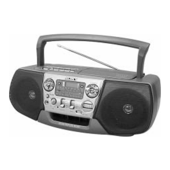
Sony CFD-V77S Service Manual
Hide thumbs
Also See for CFD-V77S:
- Operating instructions (2 pages) ,
- Service manual (38 pages) ,
- Operating instructions manual (52 pages)
Table of Contents
Advertisement
SERVICE MANUAL
Ver 1.1 1999. 05
CD player section
System
Compact disc digital audio system
Laser diode properties
Material: GaAlAs
Wavelength:780 nm
Emission duration : Continuous
Laser output : Less than 44.6 µW
(This output is the value measured at a
distance of about 200 mm from the objective
lens surface on the optical pick-up block
with 7 mm aperture.)
Spindle speed
200 r/min (rpm) to 500 r/min (rpm) (CLV)
Number of channels
2
Frequency response
20 – 20,000 Hz + 1/-2 dB
Wow and flutter
Below measurable limit
Radio section
Frequency range
FM Italy
MW Italy
SW1
SW2
IF
FM
AM/MW : 455 kHz
Aerials
FM
MW
MICROFILM
SPECIFICATIONS
87.5 – 108 MHz
Other European
87.6 – 107 MHz
models and Saudi Arabia
Other models
87.6 – 108 MHz
526.5 – 1,606.5 kHz
Other European
531 – 1,602 kHz
models and Saudi Arabia
Other models
530 – 1,605 kHz or
531 – 1,602 kHz
2.3 – 7 MHz
7 – 22 MHz
: 10.7 MHz
: Telescopic aerial
: Built-in ferrite bar aerial
CFD-V77S
Model Name Using Similar Mechanism
CD
CD Mechanism Type
Section
Optical Pick-up Name
Tape deck
Model Name Using Similar Mechanism
Section
Tape Transport Mechanism Type
Cassette-corder section
Recording system
Fast winding time
Frequency response
General
Speakers
Outputs
Maximum power output
Power requirements
Power consumption
CD RADIO CASSETTE-CORDER
AEP Model
E Model
CFD-V17
KSM-213CDM
KSS-213C
CFD-V17
MF-V10-117
4 -track 2 channel stereo
Approx. 120 s (sec.) with Sony cassette C-60
TYPE I (normal) : 70 – 10,000 Hz
Full range : 10 cm dia., 6 Ω, cone type (2)
Headphones jack (stereo minijack)
For 16 – 68 Ω impedance headphones
4.5 W + 4.5 W
For CD radio cassette-corder
Europe
230 V AC, 50 Hz
Other countries
110 – 120, 220 – 240 V AC selectable, 50/60
Hz or 230 V AC, 50 Hz
9 V DC, 6 R20 (size D) batteries
AC 25 W
— Continued on next page —
Advertisement
Chapters
Table of Contents

Related Manuals for Sony CFD-V77S


Summary of Contents for Sony CFD-V77S
- Page 1 Recording system 4 -track 2 channel stereo Laser diode properties Material: GaAlAs Fast winding time Approx. 120 s (sec.) with Sony cassette C-60 Wavelength:780 nm Frequency response TYPE I (normal) : 70 – 10,000 Hz Emission duration : Continuous Laser output : Less than 44.6 µW General Full range : 10 cm dia., 6 Ω, cone type (2)
-
Page 2: Table Of Contents
···························································· 3 FM recording 2. GENERAL ·········································································· 4 Sony R20P : approx. 3.5 h Sony alkaline LR20 : approx. 10 h 3. DISASSEMBLY Tape playback 3-1. Front Cabinet Assy ····························································· 5 Sony R20P : approx. 1.5 h 3-2. Control Board ····································································· 6 Sony alkaline LR20 : approx. -
Page 3: Service Notes
SECTION 1 SERVICE NOTES Laser component in this product is capable NOTES ON HANDLING THE OPTICAL PICK-UP of emitting radiation exceeding the limit for BLOCK OR BASE UNIT Class 1. The laser diode in the optical pick-up block may suffer electrostatic breakdown because of the potential difference generated by the charged electrostatic load, etc., on clothing and the human body. -
Page 4: General
SECTION 2 GENERAL LOCATION AND FUNCTION OF CONTROLS MAIN UNIT @™ @¡ @º !ª !• !¶ !§ !∞ !¢ !™ !£ @£ !¡ Tape operation buttons Battery compartment !º button TUNE knob !¡ · button CD = button !™ button DIAL !£... -
Page 5: Disassembly
SECTION 3 DISASSEMBLY • The equipment can be removed using the following procedure. Front cabinet assy Cabinet (upper) assy Power, battery, half battery, voltage selection board Volume, lcd, Control board Mechanism deck, optical pick-up section mono st, main board Note : Follow the disassembly procedure in the numerical order given. -
Page 6: Control Board
3-2. CONTROL BOARD Front cabinet assy 5 Two screws +BVTP 2.6 × 8 2 CONTROL board 6 CD button 1 Four screws 4 Knob (TU) +BVTP 2.6 × 8 3 Screw +BVTP 2.6 × 8 3-3. CABINET (UPPER) ASSY 2 Open the cassette holder assy by 1 Three screws pressing STOP/EJECT button. -
Page 7: Power, Battery, Half Battery, Voltage Selection Board
3-4. POWER, BATTERY, HALF BATTERY, VOLTAGE SELECTION BOARD 6 Two screws +BVTP 3 × 8 8 BATTERY board 7 Two connectors 2 Plate(Transformer 4.5W), shield 4 Connector 1 Four screws +BVTP 3 × 10 9 HALF BATTERY board 5 POWER board 3 Two screws !™... -
Page 8: Mechanism Deck, Optical Pick-Up Section
3-6. MECHANISM DECK, OPTICAL PICK-UP SECTION 8 CD MOTOR board 7 Remove solder 6 Two screws 5 Two screws 3 Three screws +BVTP 3 × 10 4 Mechanism deck 9 Optical pick-up section 1 Two screws +BVTP 3 × 10 2 RECORD switch board —... -
Page 9: Dial Pointer Installation
SECTION 4 DIAL POINTER INSTALLATION Note : Follow the installation procedure in the numerical order given. 1 Align the pointer with the groove of front cabinet assy and insert it as shown in the illustration. 2 Align Knob (TU) with front cabinet and fasten the screw. Front Cabinet assy 1 Pointer Knob (TU) -
Page 10: Adjustment
SECTION 5 ADJUSTMENTS 5-1. MECHANICAL ADJUSTMENT 5-2. ELECTRICAL ADJUSTMENT PRECAUTION TAPE RECODER SECTION 0dB = 0.775V Clean the following parts with a denatured-alchool-moistened swab: Standard output level record/playback head pinch roller Output HP OUT erase head rubber belts 32 Ω capstans Load impedance Demagnetize the record/playback head with a head... -
Page 11: Tuner Section
5-3. TUNER SECTION 0 dB = 1 µV • Repeat the procedures in each adjustment several times for the • Switch Location maximum level meter indication. • The frequency coverage and tracking adjustments should be VOLUME : MAX finally done by the trimmer capacitors. MEGA BASS : OFF PRESET SOUND MODE : OFF... - Page 12 FM VCO Adjustment Procedure : FM RF SSG BLACK 10.64MHz color BLUE 10.67MHz mark 0.01 µ F 10.70MHz to FM ANT IN terminal ORANGE 10.73MHz WHITE 10.76MHz Carrier frequency : 98MHz IF frequency : According to the color of CF1. Modulation : no modulation Output level : 0.1V (100dB) 1.
- Page 13 Adjustment Location : MAIN board (Component side) SW1 Frequency SW1 Frequency Coverage Coverage SW1 Tracking Adjustment Adjustment FM Tracking Adjustment Adjustment CT10 MW Frequency SW2 Frequency Coverage Coverage Adjustment Adjustment SW2 Frequency FM VCO Coverage Adjustment Adjustment FM Frequency Coverage Adjustment FM IF Adjustment...
- Page 14 TRAVERSE Check CD SECTION This check is to be done when the optical pick-up block is replaced. Notes on Check Check Procedure: Perform the traverse check in the CD test mode. Connect the oscilloscope to test point TP (VC) and TP (TE) on After check, be sure to exit the test mode.
-
Page 15: Reference
Focus Bias Check 5-4. REFERENCE This check is to be done when the optical block replaced. Focus/Tracking Gain Check Adjustment Location : MAIN board (Component side) Check Procedure: (See page 16) 1. Connect the oscilloscope to test point TP (VC) and TP (RF) on MAIN board. - Page 16 • Good Example • Incorrect Examples (Fundamental wave appears) VOLT/DIV : 0.2V VOLT/DIV : 100mV TIME/DIV : 2ms TIME/DIV : 1ms 100mV low tracking gain • Incorrent Examples (DC level changes more than on adjusted VOLT/DIV : 0.2V waveform) TIME/DIV : 2ms VOLT/DIV : 100mV TIME/DIV : 2ms 200mV...
-
Page 17: Diagrams
CFD-V77S SECTION 6 DIAGRAMS 6-1. CIRCUIT BOARDS LOCATION 6-2. BLOCK DIAGRAM RECORD SWITCH board CONNECTOR board POWER board BATTERY board MONO ST board HALF BATTERY board VOLUME board LCD board AEP, CEF, CET MODEL MONO ST CONTROL board CD MOTOR board... -
Page 18: Printed Wiring Board
CFD-V77S 6-3. PRINTED WIRING BOARD • Refer to page 20 for Note on Printed Wiring Board. • Refer to page 17 for Circuit Boards Location. • Semiconductor Location Ref. No. Location CONNECTOR BOARD LCD BOARD CONTROL BOARD ANT1 FM TELESCOPIC... -
Page 19: Schematic Diagram - Main Board(2/3)
CFD-V77S 6-4. SCHEMATIC DIAGRAM – MAIN BOARD (1/3) – • Refer to page 20 for Note on Schematic Diagram. • Refer to page 35 for IC Block Diagrams. The components identified by mark ! or dotted line with mark ! are critical for safety. -
Page 20: Schematic Diagram - Main Board(3/3)
CFD-V77S 6-5. SCHEMATIC DIAGRAM – MAIN BOARD (2/3) – • Refer to page 20 for Note on Schematic Diagram. • Refer to page 35 for IC Block Diagrams. 0.2V/div IC701 #£ RFO 0.5µsec/div 1.0 Vp-p IC702 ` XTAO 2V/div 50µsec/div 5 Vp-p 16.9 MHz... - Page 21 CFD-V77S 6-6. SCHEMATIC DIAGRAM – MAIN BOARD (3/3) – • Refer to page 20 for Note on Schematic Diagram. • Refer to page 35 for IC Block Diagrams. — 31 — — 32 —...
-
Page 22: Ic Pin Function Description
6-7. IC PIN FUNCTION DESCRIPTION IC702 CD DIGITAL SIGNAL PROCESSOR, LED DRIVE, SYSTEM CONTROL (CXP401-602R) Pin No. Pin name Description Pin No. Pin name Description SEIN CD SENS input. MNT3 – Not used (Open). CNIN CD SENS input. MNT1 – Not used (Open). -
Page 23: Ic Block Diagrams
• IC BLOCK DIAGRAMS IC1 CXA1538S 26 25 24 23 22 21 FM FRONT-END AM FRONT-END FM IF / MPX REG. DISCRI PD 1 IF / DET COUNTER TUNING PD 2 COUNTER INDICATOR AUTOBLEND MONO/ST MUTING SELECT BAND PASS MUTE RIPPLE DECORD AMP FILTER... - Page 24 IC701 CXA1992BR PD2 IV PD1 IV SUMMING SENS2 BIAS ↓ SENS1 LASER POWER CONTROL F IV AMP FE AMP C. OUT E IV AMP DFCT XRST LEVEL S VEE DATA FO. BIAS WINDOW MIRR COMP. ↓ ↓ TRK. GAIN WINDOW COMP. E-F BALANCE WINDOW COMP.
- Page 25 IC703 BA6898FP LEVEL SHIFT LEVEL SHIFT THERMAL SHUT DOWN DRIVER MUTE REG VOLTAGE DOWN, BIAS VOLTAGE DOWN, THERMAL SHUT DOWN MONITOR LEVEL SHIFT LEVEL SHIFT — 37 —...
-
Page 26: Exploded Views
SECTION 7 EXPLODED VIEWS NOTE: • -XX, -X mean standardized parts, so they may • Color Indication of Appearance Parts Example: When indicating parts by reference number, have some differences from the original one. KNOB, BALANCE (WHITE) . . . (RED) please include the board name. -
Page 27: Rear Cabinet Section
7-2. REAR CABINET SECTION ANT1 not supplied T901 F901 F902 Ref. No. Part No. Description Remarks Ref. No. Part No. Description Remarks 3-031-561-01 SPRING, CASSETTE UP * 64 1-672-302-11 BATTERY BOARD * 52 1-672-956-11 POWER BOARD 3-028-154-01 TERMINAL (–), BATT 4-960-167-01 SCREW (3 ×... -
Page 28: Upper Cabinet Section
7-3. UPPER CABINET SECTION S801 LCD800 not supplied Ref. No. Part No. Description Remarks Ref. No. Part No. Description Remarks * 101 A-3321-964-A MAIN BOARD, COMPLETE (EA) 3-922-112-41 DAMPER (E, EA, SP) * 101 A-3321-968-A MAIN BOARD, COMPLETE (E, SP) 3-923-736-01 COVER, CD * 101 A-3322-079-A MAIN BOARD, COMPLETE (AEP,CET) - Page 29 7-4. MECHANISM DECK SECTION (1) (MF-V10-117) HRP301 HE301 Ref. No. Part No. Description Remarks Ref. No. Part No. Description Remarks 3-933-010-01 SPRING (S/P), TORSION * 162 3-008-587-01 SLIDER (STOP) 3-933-025-01 SPRING (P), TORSION * 163 3-008-591-01 SLIDER (PAUSE) 3-933-026-01 LEVER (P) 3-933-004-01 CLAW, REEL 3-933-024-01 ROLLER, PINCH * 165...
- Page 30 7-5. MECHANISM DECK SECTION (2) (MF-V10-117) S601 M601 Ref. No. Part No. Description Remarks Ref. No. Part No. Description Remarks 3-933-029-01 LEVER, ERASING PREVENTION X-3372-924-1 FLYWHEEL ASSY 3-933-182-01 SPRING, CASSETTE 3-932-993-01 CHASSIS, OUTSERT 3-932-995-01 GEAR (MID) 3-343-358-01 RING, RETAINING X-3371-667-1 CLUTCH ASSY 3-933-005-01 SPRING (CAM), COMPRESSION 3-932-997-01 GEAR (CAM) 3-939-383-02 SPRING, COMPRESSION...
- Page 31 7-6. OPTICAL PICK-UP SECTION (KSM-213CDM) not supplied (including M702) M702 M701 Ref. No. Part No. Description Remarks Ref. No. Part No. Description Remarks 2-626-908-01 SHAFT, SLED ! 254 8-848-483-05 OPTICAL PICK-UP KSS-213C 2-627-003-02 GEAR (B)(RP) X-2626-202-1 CHASSIS ASSY (MB)(RP), MOTOR (SPINDLE) 2-626-907-01 GEAR (A)(S) (INCLUDING M702) M701...
-
Page 32: Main Section
CONNECTOR BATTERY CD MOTOR CONTROL FINE TUNING HALF BATTERY MAIN SECTION 8 ELECTRICAL PARTS LIST NOTE: • Due to standardization, replacements in the • RESISTORS • SEMICONDUCTORS parts list may be different from the parts All resistors are in ohms. In each case, u: µ, for example: specified in the diagrams or the components METAL: metal-film resistor... - Page 33 MAIN Ref. No. Part No. Description Remarks Ref. No. Part No. Description Remarks < CAPACITOR > C153 1-124-443-00 ELECT 100uF C154 1-124-443-00 ELECT 100uF 1-162-215-31 CERAMIC 47PF C155 1-104-664-11 ELECT 47uF 1-124-907-11 ELECT 10uF C156 1-136-165-00 FILM 0.1uF 1-162-205-31 CERAMIC 18PF C157 1-127-883-21 CERAMIC...
- Page 34 MAIN Ref. No. Part No. Description Remarks Ref. No. Part No. Description Remarks C710 1-162-302-11 CERAMIC 0.0022uF 20% C829 1-162-306-11 CERAMIC 0.01uF C711 1-162-202-31 CERAMIC 13PF C831 1-162-306-11 CERAMIC 0.01uF C712 1-162-294-31 CERAMIC 0.001uF C713 1-136-165-00 FILM 0.1uF < FILTER > C714 1-136-165-00 FILM 0.1uF...
- Page 35 MAIN Ref. No. Part No. Description Remarks Ref. No. Part No. Description Remarks < CABLE HOLDER > R102 1-249-404-00 CARBON 1/4W F R103 1-249-441-11 CARBON 100K 1/4W * KH306 1-565-386-11 HOLDER, CABLE 5P R104 1-247-843-11 CARBON 3.3K 1/4W * KH803 1-568-135-21 HOLDER, CABLE 7P R105 1-249-434-11 CARBON...
- Page 36 MAIN MONO ST POWER Ref. No. Part No. Description Remarks Ref. No. Part No. Description Remarks R313 1-249-393-11 CARBON 1/4W F R804 1-249-430-11 CARBON 1/4W R314 1-249-425-11 CARBON 4.7K 1/4W F R805 1-249-430-11 CARBON 1/4W R315 1-247-863-91 CARBON 1/4W R806 1-249-430-11 CARBON 1/4W R319...
- Page 37 POWER RECORD SWITCH VOLTAGE SELECTION VOLUME Ref. No. Part No. Description Remarks Ref. No. Part No. Description Remarks < CONNECTOR > 1-672-959-11 VOLUME BOARD ************* * CNP902 1-785-670-11 PIN, CONNECTOR (PC BOARD) 4P * CNP903 1-785-655-11 PIN, CONNECTOR (PC BOARD) 3P <...
- Page 38 CFD-V77S Ref. No. Part No. Description Remarks ************* HARDWARE LIST ************* 7-685-647-79 SCREW +BVTP 3 × 10 TYPE2 N-S 7-685-647-14 SCREW +BVTP 3 × 10 TYPE2 N-S 7-682-548-04 SCREW +B 3 × 8 7-621-775-20 SCREW +B 2.6 × 5 7-621-770-87 SCREW +B 2.6 × 5 7-685-648-79 SCREW +BVTP 3 ×...
- Page 39 Recording system 4 -track 2 channel stereo Laser diode properties Material: GaAlAs Fast winding time Approx. 120 s (sec.) with Sony cassette C-60 Wavelength:780 nm Frequency response TYPE I (normal) : 70 – 10,000 Hz Emission duration : Continuous Laser output : Less than 44.6 µW General Full range : 10 cm dia., 6 Ω, cone type (2)
- Page 40 ···························································· 3 FM recording 2. GENERAL ·········································································· 4 Sony R20P : approx. 3.5 h Sony alkaline LR20 : approx. 10 h 3. DISASSEMBLY Tape playback 3-1. Front Cabinet Assy ····························································· 5 Sony R20P : approx. 1.5 h 3-2. Control Board ····································································· 6 Sony alkaline LR20 : approx.
-
Page 41: Service Notes
SECTION 1 SERVICE NOTES Laser component in this product is capable NOTES ON HANDLING THE OPTICAL PICK-UP of emitting radiation exceeding the limit for BLOCK OR BASE UNIT Class 1. The laser diode in the optical pick-up block may suffer electrostatic breakdown because of the potential difference generated by the charged electrostatic load, etc., on clothing and the human body. -
Page 42: General
SECTION 2 GENERAL LOCATION AND FUNCTION OF CONTROLS MAIN UNIT @™ @¡ @º !ª !• !¶ !§ !∞ !¢ !™ !£ @£ !¡ Tape operation buttons Battery compartment !º button TUNE knob !¡ · button CD = button !™ button DIAL !£... -
Page 43: Disassembly
SECTION 3 DISASSEMBLY • The equipment can be removed using the following procedure. Front cabinet assy Cabinet (upper) assy Power, battery, half battery, voltage selection board Volume, lcd, Control board Mechanism deck, optical pick-up section mono st, main board Note : Follow the disassembly procedure in the numerical order given. -
Page 44: Control Board
3-2. CONTROL BOARD Front cabinet assy 5 Two screws +BVTP 2.6 × 8 2 CONTROL board 6 CD button 1 Four screws 4 Knob (TU) +BVTP 2.6 × 8 3 Screw +BVTP 2.6 × 8 3-3. CABINET (UPPER) ASSY 2 Open the cassette holder assy by 1 Three screws pressing STOP/EJECT button. -
Page 45: Power, Battery, Half Battery, Voltage Selection Board
3-4. POWER, BATTERY, HALF BATTERY, VOLTAGE SELECTION BOARD 6 Two screws +BVTP 3 × 8 8 BATTERY board 7 Two connectors 2 Plate(Transformer 4.5W), shield 4 Connector 1 Four screws +BVTP 3 × 10 9 HALF BATTERY board 5 POWER board 3 Two screws !™... -
Page 46: Mechanism Deck, Optical Pick-Up Section
3-6. MECHANISM DECK, OPTICAL PICK-UP SECTION 8 CD MOTOR board 7 Remove solder 6 Two screws 5 Two screws 3 Three screws +BVTP 3 × 10 4 Mechanism deck 9 Optical pick-up section 1 Two screws +BVTP 3 × 10 2 RECORD switch board —... -
Page 47: Dial Pointer Installation
SECTION 4 DIAL POINTER INSTALLATION Note : Follow the installation procedure in the numerical order given. 1 Align the pointer with the groove of front cabinet assy and insert it as shown in the illustration. 2 Align Knob (TU) with front cabinet and fasten the screw. Front Cabinet assy 1 Pointer Knob (TU) -
Page 48: Adjustment
SECTION 5 ADJUSTMENTS 5-1. MECHANICAL ADJUSTMENT 5-2. ELECTRICAL ADJUSTMENT PRECAUTION TAPE RECODER SECTION 0dB = 0.775V Clean the following parts with a denatured-alchool-moistened swab: Standard output level record/playback head pinch roller Output HP OUT erase head rubber belts 32 Ω capstans Load impedance Demagnetize the record/playback head with a head... -
Page 49: Tuner Section
5-3. TUNER SECTION 0 dB = 1 µV • Repeat the procedures in each adjustment several times for the • Switch Location maximum level meter indication. • The frequency coverage and tracking adjustments should be VOLUME : MAX finally done by the trimmer capacitors. MEGA BASS : OFF PRESET SOUND MODE : OFF... - Page 50 FM VCO Adjustment Procedure : FM RF SSG BLACK 10.64MHz color BLUE 10.67MHz mark 0.01 µ F 10.70MHz to FM ANT IN terminal ORANGE 10.73MHz WHITE 10.76MHz Carrier frequency : 98MHz IF frequency : According to the color of CF1. Modulation : no modulation Output level : 0.1V (100dB) 1.
- Page 51 Adjustment Location : MAIN board (Component side) SW1 Frequency SW1 Frequency Coverage Coverage SW1 Tracking Adjustment Adjustment FM Tracking Adjustment Adjustment CT10 MW Frequency SW2 Frequency Coverage Coverage Adjustment Adjustment SW2 Frequency FM VCO Coverage Adjustment Adjustment FM Frequency Coverage Adjustment FM IF Adjustment...
- Page 52 TRAVERSE Check CD SECTION This check is to be done when the optical pick-up block is replaced. Notes on Check Check Procedure: Perform the traverse check in the CD test mode. Connect the oscilloscope to test point TP (VC) and TP (TE) on After check, be sure to exit the test mode.
-
Page 53: Reference
Focus Bias Check 5-4. REFERENCE This check is to be done when the optical block replaced. Focus/Tracking Gain Check Adjustment Location : MAIN board (Component side) Check Procedure: (See page 16) 1. Connect the oscilloscope to test point TP (VC) and TP (RF) on MAIN board. - Page 54 • Good Example • Incorrect Examples (Fundamental wave appears) VOLT/DIV : 0.2V VOLT/DIV : 100mV TIME/DIV : 2ms TIME/DIV : 1ms 100mV low tracking gain • Incorrent Examples (DC level changes more than on adjusted VOLT/DIV : 0.2V waveform) TIME/DIV : 2ms VOLT/DIV : 100mV TIME/DIV : 2ms 200mV...
-
Page 55: Diagrams
CFD-V77S SECTION 6 DIAGRAMS 6-1. CIRCUIT BOARDS LOCATION 6-2. BLOCK DIAGRAM RECORD SWITCH board CONNECTOR board POWER board BATTERY board MONO ST board HALF BATTERY board VOLUME board LCD board AEP, CEF, CET MODEL MONO ST CONTROL board CD MOTOR board... -
Page 56: Printed Wiring Board
CFD-V77S 6-3. PRINTED WIRING BOARD • Refer to page 20 for Note on Printed Wiring Board. • Refer to page 17 for Circuit Boards Location. • Semiconductor Location Ref. No. Location CONNECTOR BOARD LCD BOARD CONTROL BOARD ANT1 FM TELESCOPIC... -
Page 57: Schematic Diagram - Main Board(2/3)
CFD-V77S 6-4. SCHEMATIC DIAGRAM – MAIN BOARD (1/3) – • Refer to page 20 for Note on Schematic Diagram. • Refer to page 35 for IC Block Diagrams. The components identified by mark ! or dotted line with mark ! are critical for safety. -
Page 58: Schematic Diagram - Main Board(3/3)
CFD-V77S 6-5. SCHEMATIC DIAGRAM – MAIN BOARD (2/3) – • Refer to page 20 for Note on Schematic Diagram. • Refer to page 35 for IC Block Diagrams. 0.2V/div IC701 #£ RFO 0.5µsec/div 1.0 Vp-p IC702 ` XTAO 2V/div 50µsec/div 5 Vp-p 16.9 MHz... - Page 59 CFD-V77S 6-6. SCHEMATIC DIAGRAM – MAIN BOARD (3/3) – • Refer to page 20 for Note on Schematic Diagram. • Refer to page 35 for IC Block Diagrams. — 31 — — 32 —...
-
Page 60: Ic Pin Function Description
6-7. IC PIN FUNCTION DESCRIPTION IC702 CD DIGITAL SIGNAL PROCESSOR, LED DRIVE, SYSTEM CONTROL (CXP401-602R) Pin No. Pin name Description Pin No. Pin name Description SEIN CD SENS input. MNT3 – Not used (Open). CNIN CD SENS input. MNT1 – Not used (Open). - Page 61 • IC BLOCK DIAGRAMS IC1 CXA1538S 26 25 24 23 22 21 FM FRONT-END AM FRONT-END FM IF / MPX REG. DISCRI PD 1 IF / DET COUNTER TUNING PD 2 COUNTER INDICATOR AUTOBLEND MONO/ST MUTING SELECT BAND PASS MUTE RIPPLE DECORD AMP FILTER...
- Page 62 IC701 CXA1992BR PD2 IV PD1 IV SUMMING SENS2 BIAS ↓ SENS1 LASER POWER CONTROL F IV AMP FE AMP C. OUT E IV AMP DFCT XRST LEVEL S VEE DATA FO. BIAS WINDOW MIRR COMP. ↓ ↓ TRK. GAIN WINDOW COMP. E-F BALANCE WINDOW COMP.
- Page 63 IC703 BA6898FP LEVEL SHIFT LEVEL SHIFT THERMAL SHUT DOWN DRIVER MUTE REG VOLTAGE DOWN, BIAS VOLTAGE DOWN, THERMAL SHUT DOWN MONITOR LEVEL SHIFT LEVEL SHIFT — 37 —...
-
Page 64: Exploded Views
SECTION 7 EXPLODED VIEWS NOTE: • -XX, -X mean standardized parts, so they may • Color Indication of Appearance Parts Example: When indicating parts by reference number, have some differences from the original one. KNOB, BALANCE (WHITE) . . . (RED) please include the board name. - Page 65 7-2. REAR CABINET SECTION ANT1 not supplied T901 F901 F902 Ref. No. Part No. Description Remarks Ref. No. Part No. Description Remarks 3-031-561-01 SPRING, CASSETTE UP * 64 1-672-302-11 BATTERY BOARD * 52 1-672-956-11 POWER BOARD 3-028-154-01 TERMINAL (–), BATT 4-960-167-01 SCREW (3 ×...
- Page 66 7-3. UPPER CABINET SECTION S801 LCD800 not supplied Ref. No. Part No. Description Remarks Ref. No. Part No. Description Remarks * 101 A-3321-964-A MAIN BOARD, COMPLETE (EA) 3-922-112-41 DAMPER (E, EA, SP) * 101 A-3321-968-A MAIN BOARD, COMPLETE (E, SP) 3-923-736-01 COVER, CD * 101 A-3322-079-A MAIN BOARD, COMPLETE (AEP,CET)
- Page 67 7-4. MECHANISM DECK SECTION (1) (MF-V10-117) HRP301 HE301 Ref. No. Part No. Description Remarks Ref. No. Part No. Description Remarks 3-933-010-01 SPRING (S/P), TORSION * 162 3-008-587-01 SLIDER (STOP) 3-933-025-01 SPRING (P), TORSION * 163 3-008-591-01 SLIDER (PAUSE) 3-933-026-01 LEVER (P) 3-933-004-01 CLAW, REEL 3-933-024-01 ROLLER, PINCH * 165...
- Page 68 7-5. MECHANISM DECK SECTION (2) (MF-V10-117) S601 M601 Ref. No. Part No. Description Remarks Ref. No. Part No. Description Remarks 3-933-029-01 LEVER, ERASING PREVENTION X-3372-924-1 FLYWHEEL ASSY 3-933-182-01 SPRING, CASSETTE 3-932-993-01 CHASSIS, OUTSERT 3-932-995-01 GEAR (MID) 3-343-358-01 RING, RETAINING X-3371-667-1 CLUTCH ASSY 3-933-005-01 SPRING (CAM), COMPRESSION 3-932-997-01 GEAR (CAM) 3-939-383-02 SPRING, COMPRESSION...
- Page 69 7-6. OPTICAL PICK-UP SECTION (KSM-213CDM) not supplied (including M702) M702 M701 Ref. No. Part No. Description Remarks Ref. No. Part No. Description Remarks 2-626-908-01 SHAFT, SLED ! 254 8-848-483-05 OPTICAL PICK-UP KSS-213C 2-627-003-02 GEAR (B)(RP) X-2626-202-1 CHASSIS ASSY (MB)(RP), MOTOR (SPINDLE) 2-626-907-01 GEAR (A)(S) (INCLUDING M702) M701...
- Page 70 CONNECTOR BATTERY CD MOTOR CONTROL FINE TUNING HALF BATTERY MAIN SECTION 8 ELECTRICAL PARTS LIST NOTE: • Due to standardization, replacements in the • RESISTORS • SEMICONDUCTORS parts list may be different from the parts All resistors are in ohms. In each case, u: µ, for example: specified in the diagrams or the components METAL: metal-film resistor...
- Page 71 MAIN Ref. No. Part No. Description Remarks Ref. No. Part No. Description Remarks < CAPACITOR > C153 1-124-443-00 ELECT 100uF C154 1-124-443-00 ELECT 100uF 1-162-215-31 CERAMIC 47PF C155 1-104-664-11 ELECT 47uF 1-124-907-11 ELECT 10uF C156 1-136-165-00 FILM 0.1uF 1-162-205-31 CERAMIC 18PF C157 1-127-883-21 CERAMIC...
- Page 72 MAIN Ref. No. Part No. Description Remarks Ref. No. Part No. Description Remarks C710 1-162-302-11 CERAMIC 0.0022uF 20% C829 1-162-306-11 CERAMIC 0.01uF C711 1-162-202-31 CERAMIC 13PF C831 1-162-306-11 CERAMIC 0.01uF C712 1-162-294-31 CERAMIC 0.001uF C713 1-136-165-00 FILM 0.1uF < FILTER > C714 1-136-165-00 FILM 0.1uF...
- Page 73 MAIN Ref. No. Part No. Description Remarks Ref. No. Part No. Description Remarks < CABLE HOLDER > R102 1-249-404-00 CARBON 1/4W F R103 1-249-441-11 CARBON 100K 1/4W * KH306 1-565-386-11 HOLDER, CABLE 5P R104 1-247-843-11 CARBON 3.3K 1/4W * KH803 1-568-135-21 HOLDER, CABLE 7P R105 1-249-434-11 CARBON...
- Page 74 MAIN MONO ST POWER Ref. No. Part No. Description Remarks Ref. No. Part No. Description Remarks R313 1-249-393-11 CARBON 1/4W F R804 1-249-430-11 CARBON 1/4W R314 1-249-425-11 CARBON 4.7K 1/4W F R805 1-249-430-11 CARBON 1/4W R315 1-247-863-91 CARBON 1/4W R806 1-249-430-11 CARBON 1/4W R319...
- Page 75 POWER RECORD SWITCH VOLTAGE SELECTION VOLUME Ref. No. Part No. Description Remarks Ref. No. Part No. Description Remarks < CONNECTOR > 1-672-959-11 VOLUME BOARD ************* * CNP902 1-785-670-11 PIN, CONNECTOR (PC BOARD) 4P * CNP903 1-785-655-11 PIN, CONNECTOR (PC BOARD) 3P <...
- Page 76 CFD-V77S Ref. No. Part No. Description Remarks ************* HARDWARE LIST ************* 7-685-647-79 SCREW +BVTP 3 × 10 TYPE2 N-S 7-685-647-14 SCREW +BVTP 3 × 10 TYPE2 N-S 7-682-548-04 SCREW +B 3 × 8 7-621-775-20 SCREW +B 2.6 × 5 7-621-770-87 SCREW +B 2.6 × 5 7-685-648-79 SCREW +BVTP 3 ×...
Need help?
Do you have a question about the CFD-V77S and is the answer not in the manual?
Questions and answers
جیوه اش کجاست