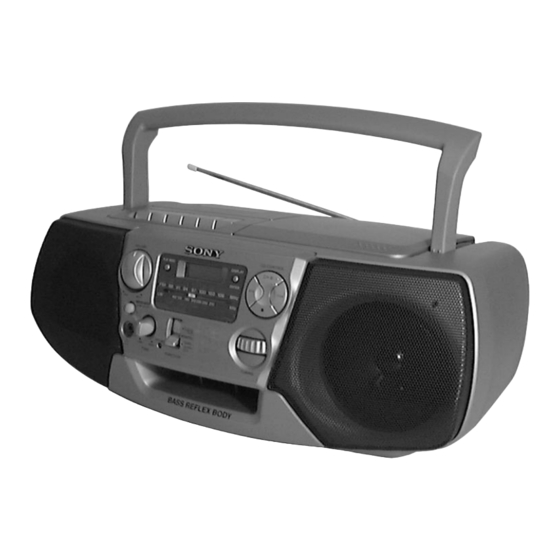
Sony CFD-V27 Service Manual
Hide thumbs
Also See for CFD-V27:
- Operating instructions manual (28 pages) ,
- Operating instructions (2 pages) ,
- Operating instructions manual (52 pages)
Table of Contents
Advertisement
SERVICE MANUAL
Ver 1.1 2000. 08
With SUPPLEMENT-1 (9-926-997-81)
CD player section
System
Compact disc digital audio system
Laser diode properties
Material: GaAlAs
Wavelength:780 nm
Emission duration : Continuous
Laser output : Less than 44.6 µW
(This output is the value measured at a
distance of about 200 mm from the objective
lens surface on the optical pick-up block
with 7 mm aperture.)
Spindle speed
200 r/min (rpm) to 500 r/min (rpm) (CLV)
Number of channels
2
Frequency response
20 – 20,000 Hz + 1/-2 dB
Wow and flutter
Below measurable limit
Radio section
Frequency range
FM : 87.6 – 108 MHz
AM : 530 –1,710 kHz
Aerials
FM : Telescopic antenna
AM : Built-in ferrite bar aerial
Cassette-corder section
Recording system
4 -track 2 channel stereo
Fast winding time
Approx. 120 s (sec.) with Sony cassette C-60
Frequency response
TYPE I (normal) : 70 – 10,000 Hz
General
Speakers
Full range : 10 cm dia., 3.2 , cone type (2)
Outputs
Headphones jack (stereo minijack)
For 16 – 68
Power output
2.3 W + 2.3 W (at 3.2 , 10 % harmonic
distortion)
MICROFILM
CD
Section
Tape deck
Section
SPECIFICATIONS
impedance headphones
CFD-V27
Model Name Using Similar Mechanism
CD Mechanism Type
Optical Pick-up Name
Model Name Using Similar Mechanism
Tape Transport Mechanism Type
Power requirements
For CD radio cassette-corder :
120V AC, 60 Hz
9V DC, 6 size D (R 20) batteries
Power consumption
AC 20W
Battery life
For CD radio cassette-corder:
FM recording
Sony R20P : approx. 13.5 h
Sony alkaline LR20 : approx. 20 h
Tape playback
Sony R20P : approx. 7.5 h
Sony alkaline LR20 : approx. 15 h
CD playback
Sony R20P : approx. 2.5 h
Sony alkaline LR20 : approx. 7 h
Dimensions
Approx. 420
5
(16
/
8
parts)
Mass
Approx. 4.1 kg (9 lb. 1 oz) (incl. batteries)
Supplied accessories
AC power cord (1)
Design and specifications are subject to change without notice.
CD RADIO CASSETTE-CORDER
E Model
CFD-V17
KSM-213CDM
KSS-213CDM
CFD-V17
MF-V10-117
165 256 mm (w/h/d)
1
1
6
/
10
/
inches) (incl. projecting
2
8
Advertisement
Chapters
Table of Contents

Related Manuals for Sony CFD-V27


Summary of Contents for Sony CFD-V27
- Page 1 4 -track 2 channel stereo Mass Approx. 4.1 kg (9 lb. 1 oz) (incl. batteries) Fast winding time Approx. 120 s (sec.) with Sony cassette C-60 Supplied accessories AC power cord (1) Frequency response TYPE I (normal) : 70 – 10,000 Hz Design and specifications are subject to change without notice.
-
Page 2: Table Of Contents
COMPONENTS IDENTIFIED BY MARK ! OR DOTTED LINE WITH MARK ! ON THE SCHEMATIC DIAGRAMS AND IN THE PARTS LIST ARE CRITICAL TO SAFE OPERATION. REPLACE THESE COMPONENTS WITH SONY PARTS WHOSE PART NUMBERS APPEAR AS SHOWN IN THIS MANUAL OR IN SUPPLEMENTS PUBLISHED BY SONY. -
Page 3: Service Notes
SECTION 1 SERVICE NOTES Laser component in this product is capable NOTES ON HANDLING THE OPTICAL PICK-UP of emitting radiation exceeding the limit for BLOCK OR BASE UNIT Class 1. The laser diode in the optical pick-up block may suffer electrostatic breakdown because of the potential difference generated by the charged electrostatic load, etc., on clothing and the human body. -
Page 4: General
SECTION 2 GENERAL LOCATION AND FUNCTION OF CONTROLS MAIN UNIT @¡ @º !ª !• !¶ !§ !∞ !¢ !£ !™ !¡ Tape operation buttons Battery compartment !º button TUNE knob !¡ · button CD = button !™ button DIAL !£ button FUNCTION switch !¢... -
Page 5: Disassembly
SECTION 3 DISASSEMBLY The equipment can be removed using the following procedure. Cabinet (upper) assy Inlet, power, battery, half battery board Front cabinet assy Control board Main board Mechanism deck, optical pick-up section Note : Follow the disassembly procedure in the numerical order given. 3-1. -
Page 6: Control Board
3-2. CONTROL BOARD Cabinet (Front) sub assy 5 Two screws +BVTP 2.6 2 CONTROL board 6 Button (CD) 1 Four screws 4 Knob (TU) 3 Screw 3-3. CABINET (UPPER) ASSY 1 Three screws +BVTP 3 5 Three screws +BVTP 3 3 Open the Lid (CD) in the direction of the arrow. -
Page 7: Inlet, Power, Battery, Half Battery Board
3-4. INLET, POWER, BATTERY, HALF BATTERY BOARD 7 Two screws 9 BATTERY board +BVTP 3 8 Two connectors 6 Connector 7 Two screws Cover +BVTP 3 1 Four screws +BVTP 3 5 Transformer, power 0 HALF BATTERY board 4 POWER board 3 INLET board 2 Two screws Rear cabinet... -
Page 8: Mechanism Deck, Optical Pick-Up Section
3-6. MECHANISM DECK, OPTICAL PICK-UP SECTION 6 CD MOTOR board 5 Remove solder 8 Two screws 7 Two screws 3 Three screws +BVTP 3 4 Mechanism deck 9 Optical pick-up section 1 Two screws +BVTP 3 2 RECORD switch board —... -
Page 9: Dial Pointer Installation
SECTION 4 DIAL POINTER INSTALLATION Note : Follow the installation procedure in the numerical order given. 1 Align the pointer with the groove of front cabinet and insert it as shown in the illustration. 2 Align Tuning knob with front cabinet and fasten the screw. Front Cabinet 1 Pointer Tuning knob B... -
Page 10: Adjustment
SECTION 5 ADJUSTMENTS 5-1. MECHANICAL ADJUSTMENT 5-2. ELECTRICAL ADJUSTMENT PRECAUTION TAPE RECODER SECTION 0dB = 0.775V Clean the following parts with a denatured-alchool-moistened swab: Standard output level record/playback head pinch roller Output HP OUT erase head rubber belts capstans Load impedance Demagnetize the record/playback head with a head Output signal level 0.25 V (–10 dB) -
Page 11: Tuner Section
5-3. TUNER SECTION 0 dB = 1 µV • Repeat the procedures in each adjustment several times for the maximum level meter indication. Switch Location • The frequency coverage and tracking adjustments should be VOLUME : MAX finally done by the trimmer capacitors. MEGA BASS : OFF PRESET SOUND MODE : OFF... - Page 12 FM VCO Adjustment Procedure : FM RF Signal generator BLACK 10.64MHz color BLUE 10.67MHz mark 0.01 F 10.70MHz FM ANT IN terminal ORANGE 10.73MHz Carrier frequency : 98MHz WHITE 10.76MHz IF frequency : According to the color of CF1. Modulation : no modulation Output level : 0.1V (100dB) 1.
- Page 13 Adjustment Location : MAIN board (Component side) FM Frequency Coverage AM IF Adjustment Adjustment FM Tracking Adjustment AM Frequency Coverage Adjustment FM VCO Adjustment FM ANT IN FM IF AM Tracking Adjustment Adjustment Adjustment Location : MAIN board (Conductor side) Set the CT2 (FM OSC) and CT4 (AM OSC) trimmers to their extreme outside.
- Page 14 TRAVERSE Check CD SECTION This check is to be done when the optical pick-up block is replaced. Notes on Check Check Procedure: Perform the traverse check in the CD test mode. Connect the oscilloscope to test point TP (VC) and TP (TE) on After check, be sure to exit the test mode.
-
Page 15: Reference
Focus Bias Check 5-4. REFERENCE This check is to be done when the optical block replaced. Focus/Tracking Gain Check Adjustment Location : MAIN board (Component side) Check Procedure: (See page 16) 1. Connect the oscilloscope to test point TP (VC) and TP (RF) on MAIN board. - Page 16 • Good Example • Incorrect Examples (Fundamental wave appears) VOLT/DIV : 0.2V VOLT/DIV : 100mV TIME/DIV : 2ms TIME/DIV : 1ms 100mV low tracking gain • Incorrent Examples (DC level changes more than on adjusted VOLT/DIV : 0.2V waveform) TIME/DIV : 2ms VOLT/DIV : 100mV TIME/DIV : 2ms 200mV...
-
Page 17: Block Diagram
CFD-V27 SECTION 6 DIAGRAMS 6-1. CIRCUIT BOARDS LOCATION 6-2. BLOCK DIAGRAM MAIN BOARD RECORD SWITCH board KH308 KH307 KH307 KH308 CONNECTOR board INLET board KH307 KH306 L1, CT1 BATTERY board FM TRACKING KH306 KH307 HALF BATTERY board VOLUME BOARD L2, CT2... -
Page 18: Printed Wiring Board
CFD-V27 6-3. PRINTED WIRING BOARD • Refer to page 20 for Note on Printed Wiring Board. • Refer to page 17 for IC Circuit Board Location. • Semiconductor Location Ref. No. Location D301 G-10 D302 D-10 D303 D304 D307 D308... -
Page 19: Schematic Diagram - Main Section(1/2)
CFD-V27 6-4. SCHEMATIC DIAGRAM – MAIN SECTION (1/2) – • Refer to page 20 for Note on Schematic Diagram. • Refer to page 35 for IC Block Diagrams. • Waveform CNP301 2 REC MODE C313 10V/div 10 sec/div 55.2kHz 30Vp-p —... -
Page 20: Schematic Diagram - Main Section(2/2)
CFD-V27 • Waveform 6-5. SCHEMATIC DIAGRAM – MAIN SECTION (2/2) – • Refer to page 20 for Note on Schematic Diagram. • Refer to page 35 for IC Block Diagrams. 0.2V/div IC701 #£ RFO 0.5 sec/div 1.0 Vp-p IC702 `... - Page 21 6-6. IC PIN FUNCTION DESCRIPTION IC702 CD DIGITAL SIGNAL PROCESSOR, LCD DRIVE, SYSTEM CONTROL (CXP401-602R) Pin No. Pin name Description SEIN CD SENS input. CNIN CD SENS input. DATO CD DSP command data output. XLTO Latch output. CLKO Clock output for CD DSP command. –...
- Page 22 Pin No. Pin name Description MNT3 – Not used (Open). MNT1 – Not used (Open). MNT0 – Not used (Open). – Not used (Open). DOUT – Not used (Open). EMPHI – Not used (Open). WFCK – Not used (Open). SCOR –...
- Page 23 • IC BLOCK DIAGRAMS (MAIN SECTION) IC1 CXA1238S 26 25 24 23 22 21 FM FRONT-END AM FRONT-END FM IF / MPX REG. DISCRI PD 1 IF / DET COUNTER TUNING PD 2 COUNTER INDICATOR AUTOBLEND MONO/ST MUTING SELECT BAND PASS MUTE RIPPLE DECORD AMP...
- Page 24 • IC BLOCK DIAGRAMS (CD SECTION) IC701 CXA1992BR PD2 IV PD1 IV SUMMING SENS2 BIAS SENS1 LASER POWER CONTROL F IV AMP FE AMP C. OUT E IV AMP DFCT XRST LEVEL S VEE DATA FO. BIAS WINDOW MIRR COMP. TRK.
- Page 25 IC703 BA6898FP LEVEL SHIFT LEVEL SHIFT THERMAL SHUT DOWN DRIVER MUTE REG VOLTAGE DOWN, BIAS VOLTAGE DOWN, THERMAL SHUT DOWN MONITOR LEVEL SHIFT LEVEL SHIFT — 37 —...
-
Page 26: Exploded Views
SECTION 7 EXPLODED VIEWS NOTE: • -XX, -X mean standardized parts, so they may • The mechanical parts with no reference number When indicating parts by reference number, have some differences from the original one. in the exploded views are not supplied. please include the board name. - Page 27 7-2. REAR CABINET SECTION ANT1 not supplied T901 F902 Ref. No. Part No. Description Remarks Ref. No. Part No. Description Remarks * 51 1-672-300-11 INLET BOARD 3-031-564-01 TERMINAL (ANT) * 52 1-672-301-11 POWER BOARD 3-031-540-11 HANDLE 1-533-233-31 HOLDER, FUSE * 64 1-672-302-11 BATTERY BOARD 3-031-570-11 KNOB (FUNCTION) 3-028-154-01 TERMINAL (–), BATT...
- Page 28 7-3. UPPER CABINET SECTION S801 LCD800 not supplied Ref. No. Part No. Description Remarks Ref. No. Part No. Description Remarks * 101 A-3321-916-A MAIN BOARD, COMPLETE 3-922-112-31 DAMPER 4-960-167-01 SCREW (3 8)(DIA.10), +WH 3-923-736-01 COVER, CD 3-031-560-01 SHAFT (MD) 1-777-955-11 WIRE (FLAT TYPE) (16 CORE) 3-031-545-11 BUTTON (STOP) 3-910-095-31 RUBBER, VIBRATION PROOF 3-031-543-11 BUTTON (REW)
- Page 29 7-4. MECHANISM DECK SECTION (1) (MF-V10-117) HRP301 HE301 Ref. No. Part No. Description Remarks Ref. No. Part No. Description Remarks 3-933-010-01 SPRING (S/P), TORSION * 162 3-008-587-01 SLIDER (STOP) 3-933-025-01 SPRING (P), TORSION * 163 3-008-591-01 SLIDER (PAUSE) 3-933-026-01 LEVER (P) 3-933-004-01 CLAW, REEL 3-933-024-01 ROLLER, PINCH * 165...
- Page 30 7-5. MECHANISM DECK SECTION (2) (MF-V10-117) S601 M601 Ref. No. Part No. Description Remarks Ref. No. Part No. Description Remarks 3-933-029-01 LEVER, ERASING PREVENTION X-3372-924-1 FLYWHEEL ASSY 3-933-182-01 SPRING, CASSETTE 3-932-993-01 CHASSIS, OUTSERT 3-932-995-01 GEAR (MID) 3-343-358-01 RING, RETAINING X-3371-667-1 CLUTCH ASSY 3-933-005-01 SPRING (CAM), COMPRESSION 3-932-997-01 GEAR (CAM) 3-939-383-02 SPRING, COMPRESSION...
- Page 31 7-6. OPTICAL PICK-UP SECTION (KSM-213CDM) not supplied (including M702) M702 M701 Ref. No. Part No. Description Remarks Ref. No. Part No. Description Remarks 2-626-908-01 SHAFT, SLED ! 254 8-848-483-05 OPTICAL PICK-UP KSS-213CDM 2-627-003-02 GEAR (B)(RP) X-2626-202-1 CHASSIS ASSY (MB)(RP),MOTOR(SPINDLE) 2-626-907-01 GEAR (A)(S) (INCLUDING M702) M701 X-2625-769-1 GEAR ASSY (MB)(RP),MOTOR (SLED)
-
Page 32: Electrical Parts List
CD MOTOR CONTROL BATTERY CONNECTOR RECORD SWITCH HALF BATTERY POWER SECTION 8 ELECTRICAL PARTS LIST NOTE: • Due to standardization, replacements in the • CAPACITORS: • SEMICONDUCTORS parts list may be different from the parts uF: µF In each case, u: µ, for example: specified in the diagrams or the components •... - Page 33 VOLUME DISPLAY INLET MAIN Ref. No. Part No. Description Remarks Ref. No. Part No. Description Remarks 1-672-305-11 VOLUME BOARD A-3321-916-A MAIN BOARD, COMPLETE ************* ******************** < CABLE HOLDER > 7-621-775-20 SCREW +B 2.6 5 7-685-647-79 SCREW +BVTP 3 10 TYPE2 N-S * KH307 1-568-135-21 HOLDER, CABLE 7P <...
- Page 34 MAIN Ref. No. Part No. Description Remarks Ref. No. Part No. Description Remarks C240 1-124-252-00 ELECT 0.33uF C731 1-162-215-31 CERAMIC 47PF C251 1-104-664-11 ELECT 47uF C732 1-162-306-11 CERAMIC 0.01uF C252 1-162-290-31 CERAMIC 470PF C733 1-162-282-31 CERAMIC 100PF C253 1-124-443-00 ELECT 100uF C734 1-162-282-31 CERAMIC...
- Page 35 MAIN Ref. No. Part No. Description Remarks Ref. No. Part No. Description Remarks < DIODE > < TRANSISTOR > 8-719-991-33 DIODE 1SS133T-77 8-729-036-57 TRANSISTOR KRC101M-AT 8-719-991-33 DIODE 1SS133T-77 Q101 8-729-036-80 TRANSISTOR KRC110M D301 8-719-991-33 DIODE 1SS133T-77 Q102 8-729-194-57 TRANSISTOR 2SC945-P D302 8-719-991-33 DIODE 1SS133T-77 Q103...
- Page 36 MAIN Ref. No. Part No. Description Remarks Ref. No. Part No. Description Remarks R201 1-249-431-11 CARBON 1/4W R709 1-247-883-00 CARBON 150K 1/4W R202 1-249-404-00 CARBON 1/4W F R710 1-247-885-00 CARBON 180K 1/4W R203 1-249-441-11 CARBON 100K 1/4W R711 1-247-883-00 CARBON 150K 1/4W R204...
- Page 37 MAIN Ref. No. Part No. Description Remarks < SWITCH > S351 1-571-345-11 SWITCH, LEVER SLIDE (FUNCTION) < TRANSFORMER > 1-409-944-11 COIL (DET) 1-416-522-11 COIL (IFT) T301 1-416-041-11 TRANSFORMER, BIAS OSCILLATION < VIBRATOR > X801 1-760-793-11 VIBRATOR, CERAMIC (16.9344 MHz) ************************************************************ MISCELLANEOUS ************* 1-452-899-11 MAGNET...
- Page 38 CFD-V27 Sony Corporation 99D167025-1 Printed in Singapore © 1999.4 Personal A&V Products Company 9-926-997-11 Published by Quality Engineering Dept. — 50 — (Shinagawa)
- Page 39 CFD-V27 E Model SERVICE MANUAL 2000. 08 SUPPLEMENT-1 File this supplement with the Service Manual. Subject : 1. Circuit Boards change • IC microcomputer change 2. Optional pick up block change (ECN-RCA00675) How to distinguish the sets You can distinguish the sets by the type name printed on the optical pick-up block.
-
Page 40: Adjustment
SECTION 1 ADJUSTMENT TABLE OF CONTENTS 1. ADJUSTMENT (Page 14,15) : Changed portion ································································· 2 CD SECTION 2. DIAGRAMS 2-1. BLOCK DIAGRAM ······················································· 4 Notes on Check 2-2. PRINTED WIRING BOARD ········································· 7 Perform the traverse check in the CD test mode. 2-3. -
Page 41: Diagrams
CFD-V27 SECTION 2 DIAGRAMS TRAVERSE Check Focus Bias Check 2-1. BLOCK DIAGRAM This check is to be done when the optical pick-up block is replaced. This check is to be done when the optical block replaced. MAIN BOARD Check Procedure:... -
Page 42: Printed Wiring Board
CFD-V27 2-2. PRINTED WIRING BOARD • Semiconductor Location Ref. No. Location PLAY MODE DISPLAY/ENTER D301 G-10 KSM-880DAA D303 D304 D307 D308 D309 D310 D312 1-676-118- D311 D-11 D314 D401 C-11 D801 D901 E-19 D902 E-19 (VC) D903 E-19 D904 F-19... - Page 43 CFD-V27 2-3. SCHEMATIC DIAGRAM MAIN SECTION • Refer to page 22 for IC Block Diagrams. KH308 VOLUME FUNCTION FUNCTION Note on Schematic Diagram: • All capacitors are in µF unless otherwise noted. pF: µµF The components identified by mark 0 or dotted 50 WV or less are not indicated except for electrolytics line with mark 0 are critical for safety.
- Page 44 CFD-V27 2-4. SCHEMATIC DIAGRAM MAIN SECTION • Refer to page 7 for Printed Wiring Board. • Refer to page 22 for IC Block Diagrams. • Waveforms 0.2V/div IC701 #£ RFO 0.5 sec/div 1.0 Vp-p IC702 ` XTAO 2V/div 50 sec/div 5 Vp-p 16.9 MHz...
-
Page 45: Ic Pin Function Description
2-5. IC PIN FUNCTION DESCRIPTION • MAIN BOARD IC702 CXD2587Q CD DIGITAL SIGNAL PROCESSOR Pin No. Pin Name Description SQSO SubQ 80 bit and PCM peak, level data output. CD TEXT data output SQCK Clock input for SQSO read out XRST System reset Resets at "L"... - Page 46 Pin No. Pin Name Description IGEN Constant-current input for OP amplifier — Analog power supply ASYO EFM full swing output ("L" = Vss, "H" = VDD) ASYI Asymmetry comparator voltage input BIAS Asymmetry circuit constant-current input RFAC EFM signal input —...
- Page 47 • MAIN BOARD IC801 CXP83516-605Q LCD DRIVE/SYSTEM CONTROL Pin No. Pin Name Description SCOR Sub-code sync detection signal DOOR CD lid detection H: OPEN L: CLOSE MUTE Audio signal MUTE H: MUTE ON L: MUTE OFF — Not used (OPEN) SENS SENS signal SCLK...
-
Page 48: Ic Block Diagrams
2-5. IC BLOCK DIAGRAMS IC1 CXA1238S 28 27 26 25 24 23 22 21 FM FRONT-END AM FRONT-END FM IF/ MPX REG. DISCRI IF/DET COUNTER TUNING COUNTER INDICATOR AUTOBLEND MONO/ST MUTING SELECT BAND PASS MUTE RIPPLE DECODER AMP FILTER 13 14 15 IC301 TA2068N LOGIC MONITOR... - Page 49 IC701 CXA2568M APC PD AMP LC/PD LD_ON HOLD AGCVTH VREF APC LD AMP HOLD_SW AGCCONT (50%/30% OFF) RF_BOT RFTC RF SUMMING AMP RF_EQ_AMP RF_1 ERROR AMP FOCUS TRACKING ERROR AMP VC BUFFER IC702 CXD2587Q ERROR ASYMMETRY DIGITAL DIGITAL CORRECTOR CORRECTION LRCK OPERATIONAL AMPLIFIER...
-
Page 50: Exploded Views
SECTION 3 EXPLODED VIEWS • DIFFERENT PARTS LIST Page Ref.No. Before Change After Change Part No. Description Remarks Part No. Description Remarks 1-673-259-11 CONNECTOR BOARD 1-676-124-11 CONNECTOR BOARD 1-672-304-11 CONTROL BOARD 1-676-119-11 CONTROL BOARD * 51 1-672-300-11 INLET BOARD 1-676-116-11 INLET BOARD 1-672-301-11 POWER BOARD... - Page 51 (Page 43) 7-6. OPTICAL PICK-UP SECTION (KSM-880DAA) Ref. No. Part No. Description Remarks 0 251 8-820-095-04 OPTICAL PICK-UP BLOCK (KSM-880DAA) The components identified by mark 0 or dotted line with mark 0 are critical for safety. Replace only with part number specified. —...
-
Page 52: Electrical Parts List
BATTERY CD MOTOR CONNECTOR CONTROL DISPLAY HALF BATTERY INLET MAIN SECTION 4 ELECTRICAL PARTS LIST NOTE: • Due to standardization, replacements in the • CAPACITORS: • SEMICONDUCTORS parts list may be different from the parts uF: µF In each case, u: µ, for example: specified in the diagrams or the components •... - Page 53 MAIN Ref. No. Part No. Description Remarks Ref. No. Part No. Description Remarks < CAPACITOR > C255 1-136-165-00 FILM 0.1uF 5.00% 50V C257 1-127-883-31 CERAMIC 0.039uF 1-162-215-31 CERAMIC 47PF C258 1-162-302-11 CERAMIC 0.0022uF 20.00% 16V 1-162-306-11 CERAMIC 0.01uF 20.00% 16V C301 1-104-665-11 ELECT 100uF...
- Page 54 MAIN Ref. No. Part No. Description Remarks Ref. No. Part No. Description Remarks C740 1-126-963-11 ELECT 4.7uF 20.00% 50V < IC > C741 1-126-963-11 ELECT 4.7uF 20.00% 50V C742 1-162-306-11 CERAMIC 0.01uF 20.00% 16V 8-752-050-20 IC CXA1238S C743 1-162-282-31 CERAMIC 100PF IC301 8-759-264-71 IC TA2068N...
- Page 55 MAIN Ref. No. Part No. Description Remarks Ref. No. Part No. Description Remarks R106 1-249-421-11 CARBON 2.2K 1/4W F R415 1-249-425-11 CARBON 4.7K 1/4W F R109 1-249-426-11 CARBON 5.6K 1/4W R701 1-247-893-11 CARBON 390K 1/4W R110 1-247-807-31 CARBON 1/4W R702 1-249-429-11 CARBON 1/4W R121...
- Page 56 CFD-V27 MAIN POWER RECORD SWITCH VOLUME Ref. No. Part No. Description Remarks Ref. No. Part No. Description Remarks < VARIABLE RESISTOR > 1-676-115-11 RECORD SWITCH BOARD ********************* 1-228-995-00 RES, ADJ, METAL22K RV351 1-225-438-11 RES, VAR, CARBON 20K/20K (TONE) < CONNECTOR >...
Need help?
Do you have a question about the CFD-V27 and is the answer not in the manual?
Questions and answers