Table of Contents
Advertisement
Quick Links
Advertisement
Table of Contents

Subscribe to Our Youtube Channel
Related Manuals for Aaeon FSB-868G


Summary of Contents for Aaeon FSB-868G
- Page 1 F S B - 8 6 8 G R e v . B FSB-868G Rev.B ® ® Intel Core 2 Duo/ ® ® Pentium -D/ Pentium LGA 775 Processor Full-size CPU Card With DDRII, Ethernet, ISA/ PCI/ PCI Express FSB-868G Rev.B Manual 1st Ed. Nov. 2007...
-
Page 2: Copyright Notice
AAEON assumes no liabilities resulting from errors or omissions in this document, or from the use of the information contained herein. AAEON reserves the right to make changes in the product design without notice to its users. - Page 3 F u l l - s i z e C P U C a r d F S B - 8 6 8 G R e v . B Acknowledgments All other products’ name or trademarks are properties of their respective owners.
-
Page 4: Packing List
CPU Cooler Fan for LGA 775 ® Pentium 4 3.6G Quick Installation Guide CD-ROM for manual (in PDF format) and drivers FSB-868G Rev.B CPU Card If any of these items should be missing or damaged, please contact your distributor or sales representative immediately. -
Page 5: Table Of Contents
F u l l - s i z e C P U C a r d F S B - 8 6 8 G R e v . B Contents Chapter 1 General Information 1.1 Introduction..............1-2 1.2 Feature ..............1-4 1.3 Specification .............. - Page 6 F u l l - s i z e C P U C a r d F S B - 8 6 8 G R e v . B 2.18 LAN LED Connector (CN2, CN5)......2-12 2.19 PCI-Express 【x 1】Connector (CN3) ....2-12 2.20 LVDS Channel Connector (CN4) ......
-
Page 7: Chapter 1 General Information
F u l l - s i z e C P U C a r d F S B - 8 6 8 G R e v . B Chapter General Information Chapter 1 General Information... -
Page 8: Introduction
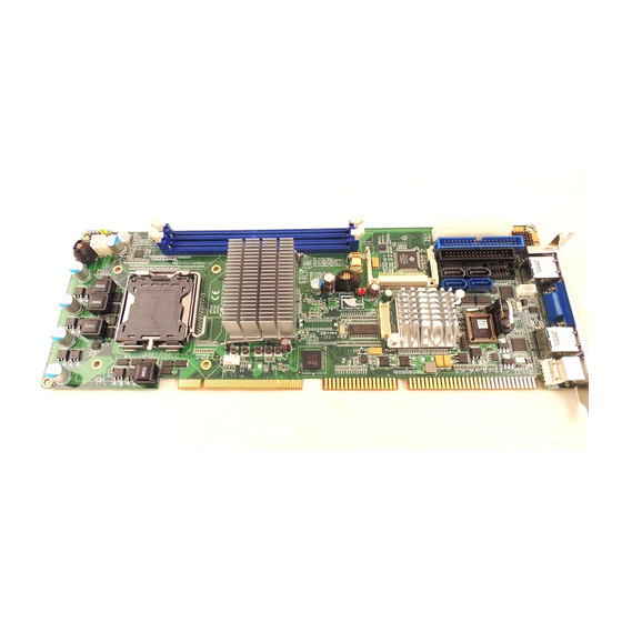
F u l l - s i z e C P U C a r d F S B - 8 6 8 G R e v . B 1.1 Introduction AAEON announces a new full-size form factor Single Board Computer (SBC) - FSB-868G Rev.B, which is based on the ® ® ®... -
Page 9: Feature
F u l l - s i z e C P U C a r d F S B - 8 6 8 G R e v . B versatile expansion interfaces bring FSB-868G Rev.B a great flexibility to serve different application demands. Furthermore,... -
Page 10: Specification
F u l l - s i z e C P U C a r d F S B - 8 6 8 G R e v . B 1.3 Specification System ® CPU: Supports Intel Core 2 Duo/ ® ®... - Page 11 F u l l - s i z e C P U C a r d F S B - 8 6 8 G R e v . B BIOS – 4Mb ROM Audio (Daughter board): Realtek ALC655 AC97 Codec, MIC-in/ Line-in/ Line-out/ CD- in optional IDE Interface:...
- Page 12 F u l l - s i z e C P U C a r d F S B - 8 6 8 G R e v . B FDD Interface: Standard FDD port x 1 (supports up to 1 floppy device) Serial Port: Two COM ports: (Internal...
-
Page 13: Chapter 2 Quick Installation Guide
F u l l - s i z e C P U C a r d F S B - 8 6 8 G R e v . B Chapter Quick Installation Guide Notice: The Quick Installation Guide is derived from Chapter 2 of user manual. -
Page 14: Safety Precautions
F u l l - s i z e C P U C a r d F S B - 8 6 8 G R e v . B 2.1 Safety Precautions Always completely disconnect the power cord from your board whenever you are working on it. -
Page 15: Location Of Connectors And Jumpers
F u l l - s i z e C P U C a r d F S B - 8 6 8 G R e v . B 2.2 Location of Connectors and Jumpers 2 - 3 Chapter 2 Quick Installation Guide... -
Page 16: Mechanical Drawing
F u l l - s i z e C P U C a r d F S B - 8 6 8 G R e v . B 2.3 Mechanical Drawing 2 - 4 Chapter 2 Quick Installation Guide... -
Page 17: List Of Jumpers
F u l l - s i z e C P U C a r d F S B - 8 6 8 G R e v . B 2.4 List of Jumpers The board has a number of jumpers that allow you to configure your system to suit your application. -
Page 18: List Of Connectors
F u l l - s i z e C P U C a r d F S B - 8 6 8 G R e v . B 2.5 List of Connectors The board has a number of connectors that allow you to configure your system to suit your application. - Page 19 F u l l - s i z e C P U C a r d F S B - 8 6 8 G R e v . B DIMM1, 2 DDRII Memory Slot FAN1 4-pin Fan Connector LVDS Channel Connector PCI Express x1 Connector AC97 Connector LAN 1 Active LED Connector...
-
Page 20: Setting Jumpers
F u l l - s i z e C P U C a r d F S B - 8 6 8 G R e v . B 2.6 Setting Jumpers You configure your card to match the needs of your application by setting jumpers. -
Page 21: Clear Cmos (Jp1)
F u l l - s i z e C P U C a r d F S B - 8 6 8 G R e v . B 2.7 LCD Voltage Selection (JP1) Function Close1-2 Close2-3 +3.3V 2.8 Clear CMOS (JP2) Function Open Protected... -
Page 22: Rs-232/422/485 Serial Port Connector (Com2)
F u l l - s i z e C P U C a r d F S B - 8 6 8 G R e v . B External Speaker(-) I2C Bus SMB Data Note: Pin 5, 7 closed: Internal Buzzer Enable 2.12 RS-232 Serial Port Connector (COM1) Signal Signal... -
Page 23: Lpt Port Connector (Lpt1)
F u l l - s i z e C P U C a r d F S B - 8 6 8 G R e v . B 2.15 LPT Port Connector (LPT1) Signal Signal #STROBE #AFD DATA0 #ERROR DATA1 #INIT DATA2... -
Page 24: Fan Connector (Fan1)
F u l l - s i z e C P U C a r d F S B - 8 6 8 G R e v . B 2.17 Fan Connector (FAN1) Signal +12V or +5V Speed Sense FAN Out Control 2.18 LVDS Channel Connector (CN1) Signal Signal... -
Page 25: Pci-Express 【X 1】Connector (Cn3)
F u l l - s i z e C P U C a r d F S B - 8 6 8 G R e v . B 2.19 PCI-Express[x1]Connector (CN2) Signal Signal +3.3V PCIe-RX1 +3.3V PCIe-RX1# PCIe-WAKE# PCIe-RST# PCIe-CLK1 +3.3VSB PCIe-CLK1#... -
Page 26: Ps2 Keyboard/Mouse Connector (Cn7)
F u l l - s i z e C P U C a r d F S B - 8 6 8 G R e v . B 2.21 LAN LED Connector (CN4, CN7) Signal Signal Active_LED(+) Active_LED(-) 2.22 ATX Power Control Connector (CN5) Signal PS-ON 5VSB... - Page 27 F u l l - s i z e C P U C a r d F S B - 8 6 8 G R e v . B Below Table for China RoHS Requirements 产品中有毒有害物质或元素名称及含量 AAEON Main Board/ Daughter Board/ Backplane 有毒有害物质或元素 部件名称 铅...
-
Page 28: Chapter 3 Cpu, Heatsink And Fan Installation
F u l l - s i z e C P U c a r d F S B - 8 6 8 G R e v . B Chapter CPU, Heatsink and Fan Installation Chapter 3 CPU, Heatsink and Fan Installation... -
Page 29: Cpu Installation And Motherboard Handling
F u l l - s i z e C P U c a r d F S B - 8 6 8 G R e v . B 3.1 CPU installation and motherboard handling Note: When integrating a Pentium 4 processor-based system, be sure to take the proper electrostatic discharge (ESD) precautions. - Page 30 F u l l - s i z e C P U c a r d F S B - 8 6 8 G R e v . B b. Rotate Load Plate to fully open position c. Remove the Protective Cover Caution: Do not touch the Socket Contacts.
- Page 31 F u l l - s i z e C P U c a r d F S B - 8 6 8 G R e v . B Step 2: (Processor Handling) Note: Handle Processor by substrate edges only. Caution: Do not touch processor contacts at any time a.
- Page 32 F u l l - s i z e C P U c a r d F S B - 8 6 8 G R e v . B Step 3: (Positioning the CPU into socket) a. Grasp the processor with your thumb and forefinger on the edges with the orientation notches.
- Page 33 F u l l - s i z e C P U c a r d F S B - 8 6 8 G R e v . B d. Close the upper plate (A), place the load lever back to the original position and tightly wedge the lever into the fastening tab.
- Page 34 F u l l - s i z e C P U c a r d F S B - 8 6 8 G R e v . B b. Viewing the board again from the topside make sure the bracket on the solder side has not shifted from its position.
- Page 35 F u l l - s i z e C P U c a r d F S B - 8 6 8 G R e v . B d. Fasten the four screws. First fasten the two screws (yellow) and then fasten the two screws (red) in sequence to secure the heatsink in place.
-
Page 36: Chapter 4 Award Bios Setup
F u l l S i z e C P U C a r d F S B - 8 6 8 G R e v . B Chapter Award BIOS Setup Chapter 4 Award BIOS Setup 4-1... - Page 37 3. The CMOS memory has lost power and the configuration information has been erased. The FSB-868G Rev.B CMOS memory has an integral lithium battery backup for data retention. However, you will need to replace the complete unit when it finally runs down.
- Page 38 F u l l S i z e C P U C a r d F S B - 8 6 8 G R e v . B 4.2 Award BIOS Setup Awards BIOS ROM has a built-in Setup program that allows users to modify the basic system configuration.
- Page 39 F u l l S i z e C P U C a r d F S B - 8 6 8 G R e v . B Advanced Chipset Features Use this menu to change the values in the chipset registers and optimize your system performance.
- Page 40 Save CMOS value changes to CMOS and exit setup. Exit Without Saving Abandon all CMOS value changes and exit setup. You can refer to the “ AAEON BIOS Item Description.pdf” file in the CD for the meaning of each setting in this chapter.
-
Page 41: Chapter 5 Driver Installation
F u l l - s i z e C P U C a r d F S B - 8 6 8 G R e v . B Chapter Driver Installation Chapter 5 Driver Installation... - Page 42 F u l l - s i z e C P U C a r d F S B - 8 6 8 G R e v . B The FSB-868G Rev.B comes with a CD-ROM that contains all drivers your need.
- Page 43 F S B - 8 6 8 G R e v . B 5.1 Installation: Insert the FSB-868G Rev.B CD-ROM into the CD-ROM Drive. And install the drivers from Step 1 to Step 5 in order. Step 1 – Install INF Driver 1.
- Page 44 F u l l - s i z e C P U C a r d F S B - 8 6 8 G R e v . B 2. Click on the Win OS folder and then double click on iata61_cd file 3.
-
Page 45: Appendix A Programming The Watchdog Timer
F u l l - s i z e C P U C a r d F S B - 8 6 8 G R e v . B Appendix Programming the Watchdog Timer Appendix A Programming the Watchdog Timer... -
Page 46: Programming
FSB-868G Rev.B utilizes W83627EHG chipset as its watchdog timer controller. Below are the procedures to complete its configuration and the AAEON intial watchdog timer program is also attached based on which you can develop customized program to fit your application. - Page 47 F u l l - s i z e C P U C a r d F S B - 8 6 8 G R e v . B (2) Modify the data of configuration registers (3) Exit the W83627EHG config Mode. Undesired result may occur if the config Mode is not exited normally.
- Page 48 F u l l - s i z e C P U C a r d F S B - 8 6 8 G R e v . B = 01 Power LED pin is drived low. = 10 Power LED pin is a 1Hz toggle pulse with 50 duty cycle.
- Page 49 F u l l - s i z e C P U C a r d F S B - 8 6 8 G R e v . B second/minutes WatchDog Timer Register III (Index=F7h, Default=00h) Bit 7 : Mouse interrupt reset Enable or Disable Watchdog Timer is reset upon a Mouse interrupt Watchdog Timer is not affected by...
-
Page 50: W83627Ehg Watchdog Timer Initial Program
F u l l - s i z e C P U C a r d F S B - 8 6 8 G R e v . B A.2 W83627EHG Watchdog Timer Initial Program Example: Setting 10 sec. as Watchdog timeout interval ;/////////////////////////////////////////////////////////////////////////////////////////////// Mov dx,2eh ;Enter W83627EHG config mode... - Page 51 F u l l - s i z e C P U C a r d F S B - 8 6 8 G R e v . B ;/////////////////////////////////////////////////////////////////////////////////////////////// Dec dx Mov al,0f5h ;CRF5 (PLED mode register) Out dx,al Inc dx In al,dx And al,not 08h...
-
Page 52: Appendix B I/O Information
F u l l - s i z e C P U C a r d F S B - 8 6 8 G R e v . B Appendix I/O Information Appendix B I/O Information... -
Page 53: I/O Address Map
F u l l - s i z e C P U C a r d F S B - 8 6 8 G R e v . B B.1 I/O Address Map Appendix B I/O Information... -
Page 54: St Mb Memory Address Map
F u l l - s i z e C P U C a r d F S B - 8 6 8 G R e v . B B.2 1 MB Memory Address Map Appendix B I/O Information... -
Page 55: Irq Mapping Chart
F u l l - s i z e C P U C a r d F S B - 8 6 8 G R e v . B B.3 IRQ Mapping Chart B.4 DMA Channel Assignments Appendix B I/O Information...
Need help?
Do you have a question about the FSB-868G and is the answer not in the manual?
Questions and answers