Table of Contents

Related Manuals for Aaeon FSB-H81H


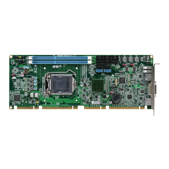
Summary of Contents for Aaeon FSB-H81H
- Page 1 F S B - H 8 1 H FSB-H81H ® Intel Core i7/i5/i3 LGA 1150 Processor Full-size CPU Card With DDR3/L, 2 Gigabit Ethernet USB 3.0/ USB2.0 SATA 6.0Gb/s, SATA 3.0 Gb/s FSB-H81H Manual Rev.A 1st Ed. August 15, 2014...
-
Page 2: Copyright Notice
AAEON assumes no liabilities resulting from errors or omissions in this document, or from the use of the information contained herein. AAEON reserves the right to make changes in the product design without notice to its users. - Page 3 F u l l - s i z e S B C F S B - H 8 1 H Acknowledgments All other products’ name or trademarks are properties of their respective owners. AMI is a trademark of American Megatrends Inc. ®...
-
Page 4: Packing List
1 USB Cable with two USB 2.0 connectors 4 SATA Cables DVD-ROM for manual (in PDF format) and Drivers FSB-H81H If any of these items should be missing or damaged, please contact your distributor or sales representative immediately. -
Page 5: Table Of Contents
F u l l - s i z e S B C F S B - H 8 1 H Contents Chapter 1 General Information 1.1 Introduction ..............1-2 1.2 Features ..............1-3 1.3 Specifications ............1-4 Chapter 2 Quick Installation Guide 2.1 Safety Precautions ............ - Page 6 F u l l - s i z e S B C F S B - H 8 1 H 2.16 COM Port 4 (CN5) ........... 2-12 2.17 COM Port 3 (CN6) ........... 2-12 2.18 COM Port 2 (RS232/485/422) (CN7) ...... 2-13 2.19 COM Port 1 (RS232/485/422) (CN8) ......
- Page 7 F u l l - s i z e S B C F S B - H 8 1 H 2.41 DDR3/DDR3L DIMM Slot (DIMM2) ......2-32 Chapter 3 AMI BIOS Setup 3.1 System Test and Initialization........3-2 3.2 AMI BIOS Setup ............3-3 Chapter 4 Driver Installation 4.1 Installation ..............
-
Page 8: Chapter 1 General Information
F u l l - s i z e S B C F S B - H 8 1 H Chapter General Information Chapter 1 General Information... -
Page 9: Introduction
H81 chipset and the Intel generation Core™ i7/i5/i3 LGA 1150 processor, to fulfill the increasing demands of multi-core processing. In a PICMG 1.3 SHB Express form factor the FSB-H81H system ® host board takes full advantage of the Intel H81 chipset for enhanced system performance and generous expansion capabilities. -
Page 10: Features
PICMG 1.3 ATX 2.1 Power Requirement Note: When FSB-H81H is accompanied external Gigabit Ethernet card through PCIe slots on backplane, the Ethernet works smoothly. However, when both Gigabit Ethernet ports are used simultaneously, the Ethernet performance may be decreasing. -
Page 11: Specifications
F u l l - s i z e S B C F S B - H 8 1 H 1.3 Specification System Form Factor PICMG 1.3 Full size SBC ® Processor Intel Generation Core i7/i5/i3 LGA 1150 Processor ... - Page 12 F u l l - s i z e S B C F S B - H 8 1 H MTBF (Hours) 60,000 Display ® Chipset Intel ® Graphic Engine Integrated Intel HD Graphics Resolution Up to 2048x1536 @ 75Hz for CRT ...
-
Page 13: Chapter 2 Quick Installation Guide
F u l l - s i z e S B C F S B - H 8 1 H Chapter Quick Installation Guide 2 - 1 Chapter 2 Quick Installation Guide... -
Page 14: Safety Precautions
F u l l - s i z e S B C F S B - H 8 1 H 2.1 Safety Precautions Always completely disconnect the power cord from your board whenever you are working on it. Do not make connections while the power is on, because a sudden rush of power can damage sensitive electronic components. -
Page 15: Location Of Connectors And Jumpers
F u l l - s i z e S B C F S B - H 8 1 H 2.2 Location of Connectors and Jumpers 2 - 3 Chapter 2 Quick Installation Guide... -
Page 16: Mechanical Drawing
F u l l - s i z e S B C F S B - H 8 1 H 2.3 Mechanical Drawing 2 - 4 Chapter 2 Quick Installation Guide... -
Page 17: List Of Jumpers
F u l l - s i z e S B C F S B - H 8 1 H 2.4 List of Jumpers The board has a number of jumpers that allow you to configure your system to suit your application. The table below shows the function of each of the board's jumpers: Jumpers Label... - Page 18 F u l l - s i z e S B C F S B - H 8 1 H COM Port 2 (RS232/422/485) COM Port 1 (RS232/422/485) USB 2.0 Port 2/3 CN12 Digital IO Port CN13 High Definition Audio CN14 PS/2 Keyboard/Mouse CN15...
-
Page 19: Setting Jumpers
F u l l - s i z e S B C F S B - H 8 1 H 2.6 Setting Jumpers You configure your card to match the needs of your application by setting jumpers. A jumper is the simplest kind of electric switch. It consists of two metal pins and a small metal clip (often protected by a plastic cover) that slides over the pins to connect them. -
Page 20: Com1 Ri/+5/+12V Selection (Cn10)
F u l l - s i z e S B C F S B - H 8 1 H 2.7 COM1 RI/+5/+12V Selection (CN10) +12V Ring CN10 Function +12V Ring (Default) 2.8 COM2 RI/+5/+12V Selection (CN11) +12V Ring CN11 Function +12V Ring (Default) -
Page 21: Cmos Rtc Setting (Cn29)
F u l l - s i z e S B C F S B - H 8 1 H CN24 Function Power ON by Button (Default) Auto Power ON 2.10 CMOS RTC Setting (CN29) 1 2 3 1 2 3 Normal Clear CMOS CN29... -
Page 22: Front Panel Connector 2 (Cn2)
F u l l - s i z e S B C F S B - H 8 1 H Signal Signal PWR_BTN (+) H/W RESET (+) PWR_BTN (-) H/W RESET (-) HDD_LED (+) PWR_LED (+) HDD_LED (-) PWR_LED (-) 2.13 Front Panel Connector 2 (CN2) Signal Signal... -
Page 23: Com Port 5 (Cn4)
F u l l - s i z e S B C F S B - H 8 1 H ±9V ±9V ±9V 2.15 COM Port 5 (CN4) Pin Name Signal Type Signal Level ±9V ±9V ±9V 2 - 11 Chapter 2 Quick Installation Guide... -
Page 24: Com Port 4 (Cn5)
F u l l - s i z e S B C F S B - H 8 1 H 2.16 COM Port 4 (CN5) Pin Name Signal Type Signal Level ±9V ±9V ±9V 2.17 COM Port 3 (CN6) 2 - 12 Chapter 2 Quick Installation Guide... -
Page 25: Com Port 2 (Rs232/485/422) (Cn7)
F u l l - s i z e S B C F S B - H 8 1 H Pin Name Signal Type Signal Level ±9V ±9V ±9V 2.18 COM Port 2 (RS232/485/422) (CN7) RS-232 Pin Name Signal Type Signal Level ±9V ±9V... - Page 26 F u l l - s i z e S B C F S B - H 8 1 H ±9V RI/+5V/+12V IN/ PWR +5V/+12V RS-422 Pin Name Signal Type Signal Level RS422_TX- RS422_TX+ RS422_RX+ RS422_RX- NC/+5V/+12V +5V/+12V RS-485 Pin Name Signal Type Signal Level RS485_D-...
-
Page 27: Com Port 1 (Rs232/485/422) (Cn8)
F u l l - s i z e S B C F S B - H 8 1 H NC/+5V/+12V +5V/+12V 2.19 COM Port 1 (RS232/485/422) (CN8) RS-232 Pin Name Signal Type Signal Level ±9V ±9V ±9V 2 - 15 Chapter 2 Quick Installation Guide... - Page 28 F u l l - s i z e S B C F S B - H 8 1 H RI/+5V/+12V IN/ PWR +5V/+12V RS-422 Pin Name Signal Type Signal Level RS422_TX- RS422_TX+ RS422_RX+ RS422_RX- NC/+5V/+12V +5V/+12V RS-485 Pin Name Signal Type Signal Level RS485_D-...
-
Page 29: Usb 2.0 Port 2/3 (Cn9)
F u l l - s i z e S B C F S B - H 8 1 H NC/+5V/+12V +5V/+12V 2.20 USB 2.0 Port 2/3 (CN9) Pin Name Signal Type Signal Level +5VSB USB2_D- DIFF USB2_D+ DIFF USB3_D+ DIFF USB3_D- DIFF... -
Page 30: Digital Io Port (Cn12)
F u l l - s i z e S B C F S B - H 8 1 H 2.21 Digital IO Port (CN12) Pin Name Signal Type Signal Level DIO1 DIO2 DIO3 DIO4 DIO5 DIO6 DIO7 DIO8 2.22 High Definition Audio (CN13) Pin Name Signal Type Signal Level... -
Page 31: Ps/2 Kb/Ms Pin Header (Cn14)
F u l l - s i z e S B C F S B - H 8 1 H HDA_SYNC HDA_SDI0 HDA_SDO AUDIO_DET# HDA_BCLK +5VSB +3.3V +3.3V 2.23 PS/2 KB/MS Pin Header (CN14) Pin Name Signal Type Signal Level KB_ DATA KB_CLK +5VSB... -
Page 32: Lpt Port (Cn15)
F u l l - s i z e S B C F S B - H 8 1 H 2.24 LPT Port (CN15) Pin Name Signal Type Signal Level STROBE# AFD# ERROR# PRINT# SLIN# 2 - 20 Chapter 2 Quick Installation Guide... -
Page 33: Sata Port 2 (Cn16)
F u l l - s i z e S B C F S B - H 8 1 H ACK# BUSY SLCT 2.25 SATA Port 2 (CN16) Pin 1 Pin 7 Pin Name Signal Type Signal Level SATA_TX4+ DIFF SATA_TX4- DIFF SATA_RX4-... -
Page 34: Sata Port 3 (Cn17)
F u l l - s i z e S B C F S B - H 8 1 H 2.26 SATA Port 3 (CN17) Pin 1 Pin 7 Pin Name Signal Type Signal Level SATA_TX5+ DIFF SATA_TX5- DIFF SATA_RX5- DIFF SATA_RX5+ DIFF... -
Page 35: Sata Port 0 (Cn19)
F u l l - s i z e S B C F S B - H 8 1 H USB0_D- DIFF USB0_D+ DIFF USB1_SSRX− DIFF USB1_SSRX+ DIFF USB1_SSTX− DIFF USB1_SSTX+ DIFF 2.28 SATA Port 0 (CN19) Pin 1 Pin 7 Pin Name Signal Type Signal Level... -
Page 36: Sata Port 1 (Cn20)
F u l l - s i z e S B C F S B - H 8 1 H 2.29 SATA Port 1 (CN20) Pin 1 Pin 7 Pin Name Signal Type Signal Level SATA_TX1+ DIFF SATA_TX1- DIFF SATA_RX1- DIFF SATA_RX1+ DIFF... -
Page 37: 100M/1G Ethernet Port 1 (Cn23)
F u l l - s i z e S B C F S B - H 8 1 H USB1_D- DIFF USB1_D+ DIFF USB2_SSRX− DIFF USB2_SSRX+ DIFF USB2_SSTX− DIFF USB2_SSTX+ DIFF 2.31 10M/100M/1G Ethernet Port 1 (CN23) ACT/LINK SPEED Pin Name Signal Type Signal Level... -
Page 38: Lpc Expansion Connector (Cn25)
F u l l - s i z e S B C F S B - H 8 1 H 2.32 LPC Expansion Connector (CN25) LAD0 LAD1 LAD2 LAD3 +3.3V LFRAME# LRESET# LCLK LDRQ0 LDRQ1 SERIRQ Pin Name Signal Type Signal Level LAD0 +3.3V... -
Page 39: Spi Programming Header (Debug Only) (Cn26)
F u l l - s i z e S B C F S B - H 8 1 H 2.33 SPI Programming Header (Debug ONLY) (CN26) Pin Name Signal Type Signal Level +3.3V +3.3V 2.34 DVI Connector (CN27) Pin Name Signal Type Signal Level TMDS_DAT2-... - Page 40 F u l l - s i z e S B C F S B - H 8 1 H VGA_DDC_CLK VGA_DDC _DATA DVI_DDC_CLK DVI_DDC_DATA VSYNC TMDS_DAT1- DIFF TMDS_DAT1+ DIFF HPLG_DETECT TMDS_DAT0- DIFF TMDS_DAT0+ DIFF TMDS_CLK+ DIFF TMDS_CLK- DIFF GREEN 2 - 28 Chapter 2 Quick Installation Guide...
-
Page 41: Vga Connector (Cn28)
F u l l - s i z e S B C F S B - H 8 1 H BLUE HSYNC GND_ANALOG 2.35 VGA Connector (CN28) Pin Name Signal Type Signal Level GREEN BLUE RED_GND_RTN GREEN_GND_RTN BLUE_GND_RTN DDC_DATA HSYNC VSYNC DDC_CLK 2 - 29... -
Page 42: Fan2 Connector (Cn30)
F u l l - s i z e S B C F S B - H 8 1 H 2.36 FAN2 Connector (CN30) Pin Name Signal Type Signal Level FAN_POWER +12V FAN_TAC FAN_CTL 2.37 FAN1 Connector (CN31) Pin Name Signal Type Signal Level FAN_POWER... -
Page 43: Atx +12V Power Connector (Cn32)
F u l l - s i z e S B C F S B - H 8 1 H 2.38 ATX +12V Power Connector (CN32) Pin Name Signal Type Signal Level +12V +12V +12V +12V 2.39 10M/100M/1G Ethernet Port 2 (CN33) ACT/LINK SPEED Pin Name... -
Page 44: Ddr3/Ddr3L Dimm Slot (Dimm1)
F u l l - s i z e S B C F S B - H 8 1 H MDI1- DIFF MDI3+ DIFF MDI3- DIFF 2.40 DDR3/DDR3L DIMM Slot (DIMM1) Standard specification. 2.41 DDR3/DDR3L DIMM Slot (DIMM2) Standard specification. 2 - 32 Chapter 2 Quick Installation Guide... - Page 45 F u l l - s i z e S B C F S B - H 8 1 H Below Table for China RoHS Requirements 产品中有毒有害物质或元素名称及含量 AAEON Main Board/ Daughter Board/ Backplane 有毒有害物质或元素 部件名称 铅 汞 镉 六价铬 多溴联苯...
-
Page 46: Chapter 3 Ami Bios Setup
F u l l - s i z e S B C F S B - H 8 1 H Chapter BIOS Setup Chapter 3 AMI BIOS Setup 3-1... -
Page 47: System Test And Initialization
4. The CMOS memory has lost power and the configuration information has been erased. The FSB-H81H CMOS memory has an integral lithium battery backup for data retention. However, you will need to replace the complete unit when it finally runs down. -
Page 48: Ami Bios Setup
F u l l - s i z e S B C F S B - H 8 1 H 3.2 AMI BIOS Setup AMI BIOS ROM has a built-in Setup program that allows users to modify the basic system configuration. This type of information is stored in battery-backed CMOS RAM and BIOS NVRAM so that it retains the Setup information when the power is turned off. -
Page 49: Setup Menu
F u l l - s i z e S B C F S B - H 8 1 H Setup Menu Setup submenu: Main Options summary: (default setting) System Date Day MM:DD:YYYY Change the month, year and century. The ‘Day’ is changed automatically. System Time HH : MM : SS Change the clock of the system. - Page 50 F u l l - s i z e S B C F S B - H 8 1 H Setup submenu: Advanced Options summary: (default setting) ACPI Settings System ACPI Parameters CPU Configuration CPU Configuration Parameters Dynamic Digital IO Dynamic Digital IO settings SATA Configuration SATA Device Options Settings...
- Page 51 F u l l - s i z e S B C F S B - H 8 1 H USB Configuration Parameters F81866 Super IO Configuration System Super IO Chip Parameters F81866 H/W Monitor Monitor hardware status S5 RTC Wake Settings Enable system to wake from S5 using RTC alarm Chapter 3 AMI BIOS Setup 3-6...
-
Page 52: Acpi Settings
F u l l - s i z e S B C F S B - H 8 1 H ACPI Settings Options summary: (default setting) Suspend Disabled S1 only (CPU Stop Clock) ACPI Sleep State S3 (Suspend to RAM) Both S1 and S3 available for OS to choose from Select the highest ACPI sleep state the system will enter when the SUSPEND button... -
Page 53: Cpu Configuration
F u l l - s i z e S B C F S B - H 8 1 H CPU Configuration Options summary: (default setting) Hyper-threading Disabled Enabled Enabled/Disabled CPU Hyper-threading function. Chapter 3 AMI BIOS Setup 3-8... - Page 54 F u l l - s i z e S B C F S B - H 8 1 H Dynamic Digital IO Options summary: (default setting) Digital Port x (GP2x) Input Direction Output Select GPIx/GPOx I/O direction Digital Port x (GP2x) Level Hi Select the output level when setting as Output ping.
-
Page 55: Sata Configuration
F u l l - s i z e S B C F S B - H 8 1 H SATA Configuration Options summary: (default setting) SATA Controller(s) Enabled Disabled Configure SATA controller operating as Legacy IDE/AHCI mode. SATA Mode Selection AHCI Configure SATA controller operating as Legacy IDE/AHCI mode. -
Page 56: Usb Configuration
F u l l - s i z e S B C F S B - H 8 1 H USB Configuration Options summary: (default setting) Legacy USB Support Enabled Disabled Auto Enables Legacy USB Support. AUTO option disables legacy support if no USB devices are connected. -
Page 57: F81866 Super Io Configuration
F u l l - s i z e S B C F S B - H 8 1 H F81866 Super IO Configuration Options summary: (default setting) Serial Port x Configuration Set Parameters of Serial Port x. Parallel Port Configuration Set Parameters of Parallel Port Chapter 3 AMI BIOS Setup 3-12... - Page 58 F u l l - s i z e S B C F S B - H 8 1 H Serial Port 1/2 Configuration Options summary: (default setting) Serial Port Disabled Enabled En/Disable specified serial port. Change Settings Auto IO=3F8h; IRQ=4; IO=3F8h;...
- Page 59 F u l l - s i z e S B C F S B - H 8 1 H RS422 RS485 Select an optimal setting for Super IO device. Chapter 3 AMI BIOS Setup 3-14...
- Page 60 F u l l - s i z e S B C F S B - H 8 1 H Serial Port 3/4/5/6 Configuration Options summary: (default setting) Serial Port Disabled Enabled En/Disable specified serial port. Change Settings Auto IO=3F8h; IRQ=4; IO=3F8h;...
-
Page 61: Parallel Port Configuration
F u l l - s i z e S B C F S B - H 8 1 H Parallel Port Configuration Options summary: (default setting) Parallel Port Disabled Enabled En/Disable Parallel port. Change Settings Auto IO=378h; IRQ=5; IO=378h; IRQ=5, 6, 7, 10, 11, IO=278h;... - Page 62 F u l l - s i z e S B C F S B - H 8 1 H IO=3BCh; IRQ=5, 6, 7, 10, 11, Select an optimal setting for Super IO device. Device Mode STD Printer Mode SPP Mode EPP-1.9 and SPP Mode EPP-1.7 and SPP Mode ECP Mode...
- Page 63 F u l l - s i z e S B C F S B - H 8 1 H F81866 H/W Monitor Options summary: (default setting) Smart Fan Function Disabled Enabled En/Disable specified Smart Fan Function Smart Fan Mode Configuration Select an optimal setting for Smart Fan.
-
Page 64: Smart Fan Mode Configuration
F u l l - s i z e S B C F S B - H 8 1 H Smart Fan Mode Configuration Options summary: (default setting) Fan1 Smart Fan Control Manual Duty Mode Auto Duty-Cycle Mode Smart Fan Mode Select Manual Duty Mode Manual mode fan control, from 1-100. -
Page 65: S5 Rtc Wake Settings
F u l l - s i z e S B C F S B - H 8 1 H S5 RTC Wake Settings Options summary: (default setting) Wake system with Fixed Disabled Time Enabled Enable or disable system wake on alarm event. When enabled, System will wake on the hr::min::sec specified. - Page 66 F u l l - s i z e S B C F S B - H 8 1 H Setup submenu: Chipset Options summary: (default setting) Power Mode ATX Type Select power supply mode. RI# Wake Disabled Enabled Enable/Disable Ring In wake up function. South Bridge South Bridge Parameters Host Bridge...
-
Page 67: South Bridge
F u l l - s i z e S B C F S B - H 8 1 H South Bridge Options summary: (default setting) Restore AC Power Loss Power Off Power On Last State Select AC power state when power is re-applied after a power failure Azalia Disabled Enabled... - Page 68 F u l l - s i z e S B C F S B - H 8 1 H PCI Express Root Port x Disabled Enabled Control the PCI Express Root Port. HP89 PCIe RTL8111E #x Disabled Enabled Control on-board LAN device Chapter 3 AMI BIOS Setup 3-23...
-
Page 69: Host Bridge
F u l l - s i z e S B C F S B - H 8 1 H Host Bridge Options summary: (default setting) Graphics Configuration Configure Graphics Settings. Chapter 3 AMI BIOS Setup 3-24... -
Page 70: Graphics Configuration
F u l l - s i z e S B C F S B - H 8 1 H Graphics Configuration Options summary: (default setting) Primary Display Auto IGFX PCIE Select which of IGFX/PEG/PCI Graphics device should be Primary Display Internal graphics Auto Disabled... - Page 71 F u l l - s i z e S B C F S B - H 8 1 H Setup submenu: Boot Options summary: (default setting) Quiet Boot Disabled Enabled En/Disable showing boot logo. Launch PXE OpROM. Disabled Enabled En/Disable PXE boot for RTL8111E LAN Boot Option #x Set the system boot order.
- Page 72 F u l l - s i z e S B C F S B - H 8 1 H Setup submenu: Security Options summary: (default setting) Administrator Password/ Not set User Password You can install a Supervisor password, and if you install a supervisor password, you can then install a user password.
- Page 73 F u l l - s i z e S B C F S B - H 8 1 H Setup submenu: Save & Exit Options summary: (default setting) Save Changes and Reset Reset the system after saving the changes Discard Changes and Reset Reset system setup without saving any changes Restore Defaults...
-
Page 74: Chapter 4 Driver Installation
F u l l - s i z e S B C F S B - H 8 1 H Chapter Driver Installation Chapter 4 Driver Installation... - Page 75 F u l l - s i z e S B C F S B - H 8 1 H The FSB-H81H comes with a DVD-ROM that contains all drivers and utilities that meet your needs. Follow the sequence below to install the drivers: Step 1 –...
- Page 76 F u l l - s i z e S B C F S B - H 8 1 H 4.1 Installation: Insert the FSB-H81H DVD-ROM into the DVD-ROM Drive. And install the drivers from Step 1 to Step 7 in order. Step 1 – Install Chipset Driver 1.
- Page 77 F u l l - s i z e S B C F S B - H 8 1 H 2. Follow the instructions that the window shows 3. The system will help you install the driver automatically Step 5 – Install LAN Driver Click on the STEP5-LAN folder and select the OS folder your system is Double click on the setup.exe file located in each OS...
- Page 78 F u l l - s i z e S B C F S B - H 8 1 H Step 7 – Install UART Driver Windows 7 Step 1: Step 2: Chapter 4 Driver Installation...
- Page 79 F u l l - s i z e S B C F S B - H 8 1 H Step 3: Step 4: Chapter 4 Driver Installation...
- Page 80 F u l l - s i z e S B C F S B - H 8 1 H Step 5: Windows 8 Step 1: Chapter 4 Driver Installation...
- Page 81 F u l l - s i z e S B C F S B - H 8 1 H Step 2: Step 3: Chapter 4 Driver Installation...
- Page 82 F u l l - s i z e S B C F S B - H 8 1 H Step 4: Step 5: Chapter 4 Driver Installation...
- Page 83 F u l l - s i z e S B C F S B - H 8 1 H Step 6: 4-10 Chapter 4 Driver Installation...
-
Page 84: Appendix A Programming The Watchdog Timer
F u l l - s i z e S B C F S B - H 8 1 H Appendix Programming the Watchdog Timer Appendix A Programming the Watchdog Timer... -
Page 85: Programming
F u l l - s i z e S B C F S B - H 8 1 H A.1 Programming FSB-H81H utilizes FINTEK 81866 chipset as its watchdog timer controller. Below are the procedures to complete its configuration and the AAEON initial watchdog timer program is also attached based on which you can develop customized program to fit your application. - Page 86 F u l l - s i z e S B C F S B - H 8 1 H There are three steps to complete the configuration setup: (1) Enter the MB PnP Mode; (2) Modify the data of configuration registers; (3) Exit the MB PnP Mode.
- Page 87 F u l l - s i z e S B C F S B - H 8 1 H Watch Dog Timer 1, 2, 3 Control Register (Index=F5h,F6h,FAh Default=00h) Appendix A Programming the Watchdog Timer...
-
Page 88: F81866 Watchdog Timer Initial Program
F u l l - s i z e S B C F S B - H 8 1 H A.2 F81866 Watchdog Timer Initial Program Main aaeonSuperIOOpen(); aaeonWdtSetCountMode(BOOL bMinute); // Set wdt count mode aaeonWdtSetTimeoutCount(BYTE tTimeout); // Set wdt timer aaeonWdtSetEnable(BOOL bEnable);... - Page 89 F u l l - s i z e S B C F S B - H 8 1 H Void aaeonWdtSetTimeoutCount(BYTE tTimeout){ f81866SetLdn(0x07); f81866WriteByte(F81866_WDT_TIME_REG, tTimeout); Void aaeonWdtSetEnable(BOOL bEnable){ f81866SetLdn(0x07); if(bEnable){ f81866WriteByte(0x30, 0x01); WDT_BASE_ADDR = (f81866ReadByte(F81866_WDT_BASEADDR_REG_MSB) << 8) | f81866ReadByte(F81866_WDT_BASEADDR_REG_LSB); WDT_STATUS = f81866ReadByte(F81866_WDT_CONTROL_REG);...
- Page 90 F u l l - s i z e S B C F S B - H 8 1 H Void aaeonSuperIOClose(){ aaeonioWritePortByte(F81866_INDEX, 0xaa); Appendix A Programming the Watchdog Timer...
-
Page 91: Appendix B I/O Information
F u l l - s i z e S B C F S B - H 8 1 H Appendix I/O Information Appendix B I/O Information... -
Page 92: I/O Address Map
F u l l - s i z e S B C F S B - H 8 1 H B.1 I/O Address Map Appendix B I/O Information... - Page 93 F u l l - s i z e S B C F S B - H 8 1 H Appendix B I/O Information...
-
Page 94: Memory Address Map
F u l l - s i z e S B C F S B - H 8 1 H B.2 Memory Address Map Appendix B I/O Information... -
Page 95: Irq Mapping Chart
F u l l - s i z e S B C F S B - H 8 1 H B.3 IRQ Mapping Chart Appendix B I/O Information... - Page 96 F u l l - s i z e S B C F S B - H 8 1 H Appendix B I/O Information...
-
Page 97: Dma Channel Assignments
F u l l - s i z e S B C F S B - H 8 1 H B.4 DMA Channel Assignments Appendix B I/O Information... -
Page 98: Appendix C Mating Connector
F u l l - s i z e S B C F S B - H 8 1 H Appendix Mating Connector C - 1 Appendix C Mating Connector... -
Page 99: List Of Mating Connectors And Cables
F u l l - s i z e S B C F S B - H 8 1 H C.1 List of Mating Connectors and Cables The table notes mating connectors and available cables. Connector Function Mating Connector Available Cable P/N Label Cable... - Page 100 F u l l - s i z e S B C F S B - H 8 1 H CN17 SATA Port PINREX 770-83-07SB39 SATA 1709070460 Cable CN18 USB 3.0 Foxconn UEA3119C-4FB Port 0 1-4F CN19 SATA Port PINREX 770-83-07SV29 SATA 1709070460 Cable...
-
Page 101: Appendix D Dio
F u l l - s i z e S B C F S B - H 8 1 H Appendix Appendix D DIO... - Page 102 F u l l - s i z e S B C F S B - H 8 1 H D.1 DIO The related register for configuring DIO is list as follows: Appendix D DIO...
- Page 103 F u l l - s i z e S B C F S B - H 8 1 H Appendix D DIO...
- Page 104 F u l l - s i z e S B C F S B - H 8 1 H Appendix D DIO...
- Page 105 F u l l - s i z e S B C F S B - H 8 1 H Appendix D DIO...
- Page 106 F u l l - s i z e S B C F S B - H 8 1 H The following is a sample code for DIO8 as input & DIO1 as output high (GPIO00, GPIO20) Outportb(0x2E,0x87); //enter configuration Outportb(0x2E,0x87);...
Need help?
Do you have a question about the FSB-H81H and is the answer not in the manual?
Questions and answers