Aiwa CSD-MD50 Service Manual
Md/cd stereo
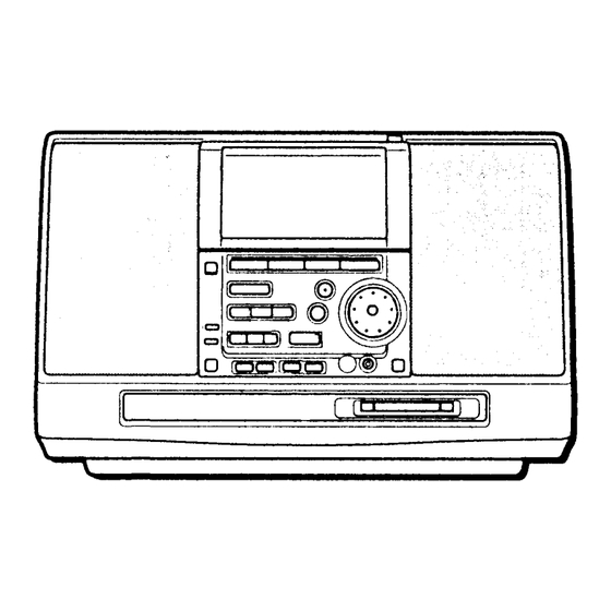
radio cassette recorder
Hide thumbs
Also See for CSD-MD50:
- Operating instructions manual (100 pages) ,
- Operating instructions manual (33 pages)
Table of Contents
Advertisement
Quick Links
Advertisement
Table of Contents

Subscribe to Our Youtube Channel
Related Manuals for Aiwa CSD-MD50


Summary of Contents for Aiwa CSD-MD50
- Page 1 CSD-MD50 SERVICE MANUAL BASIC TAPE MECHANISM : 2ZM-1R7 MD/CD STEREO BASIC MD MECHANISM : 7ZG-9B2 RADIO CASSETTE RECORDER BASIC CD MECHANISM : 3ZG-3E2 MODEL CODE : 86HR8-0117(B) 86HR8-1111(W) 86HR8-4444(L) 86HR8-8888(ST) S/M Code No. 09-994-328-4N2...
-
Page 2: Table Of Contents
TABLE OF CONTENTS SPECIFICATIONS ..........................3 ACCESSORIES/PACKAGE LIST ......................3 PROTECTION OF EYES FROM LASER BEAM DURING SERVICING ..........4 Precaution to replace Optical block......................5 DISASSEMBLY INSTRUCTIONS ...................... 6-10 ELECTRICAL MAIN PARTS LIST ....................11-15 TRANSISTOR ILLUSTRATION ......................16 FL GRID ASSIGNMENT/ANODE CONNECTION ................ -
Page 3: Specifications
SPECIFICATIONS • Design and specifications are subject to change without notice. • Dolby noise reduction manufactured under license from Dolby Laboratories Licensing Corporation. “DOLBY” and the double-D symbol are trademarks of Dolby Laboratories Licensing Corporation. • The word “BBE” and the “BBE symbol” are trademarks of BBE Sound,Inc. -
Page 4: Protection Of Eyes From Laser Beam During Servicing
PROTECTION OF EYES FROM LASER BEAM DURING SERVICING This set employs laser. Therefore, be sure to follow carefully the CAUTION instructions below when servicing. Use of controls or adjustments or performance of procedures other than those specified herein may result in hazardous WARNING! radiation exposure. -
Page 5: Precaution To Replace Optical Block
Precaution to replace Optical block (KSS-213F) Body or clothes electrostatic potential could ruin laser diode in the optical block. Be sure ground body and workbench, and use care the clothes do not touch the diode. 1) After the connection, remove solder shown in the right figure. -
Page 6: Disassembly Instructions
DISASSEMBLY INSTRUCTIONS Disassembling Procedure Remove the seven screws (A BVT2+3-18*7) and remove the rear cabinet. Remove the two screws (B BVT2+3-12*2). Remove the MAIN C.B by pulling it upward. Remove the four screws (C BVT2+3-12*4). - Page 7 Open the deck lid. Release the two claws 1 and remove the PANEL DISP by pulling it upward. Close the deck lid. Raise the deck block from the rear. Remove the two screws (D BVT2+3-12*2). While raising the MAIN C.B., release the claws starting from 1 to 7, and remove the MICOM/CD C.B.
- Page 8 How to remove the COVER, FFC. 1) Remove the five screws (A BVT2+3-12*5) and remove the deck mechanism. 2) Remove the SPR T CASS from the rib and remove the BOX CASS. 3) Release the two claws of the COVER and FFC by pressing them in the direction of the arrow.
- Page 9 4) Raise the COVER and FFC in the direction of the arrow, and remove them. How to remove FL C.B. 1) Release the two claws 2 and pull the top of the FL C.B. to the front. The FL C.B. can be removed. How to remove the CD panel 1) Move the CAM SLIDE by 1 cm to the left.
- Page 10 10. Remove the four screws A (S-SCREW, MD) and screws B HEAD, OWH RF325-74A (BVTT +3-6). Remove the four FFCs from the connector, and remove the MD MECHANISM in the direction of the arrow. (Fig-1) PLATE ASSY, SIDE L PLATE, SIDE R MD MECHANISM Fig-3 13.
-
Page 11: Electrical Main Parts List
ELECTRICAL MAIN PARTS LIST REF. NO PART NO. KANRI DESCRIPTION REF. NO PART NO. KANRI DESCRIPTION 87-020-465-080 DIODE,1SS133 (110MA) 87-A40-348-080 ZENER,MTZJ3.3A 87-020-454-010 IC,DM6851 87-A40-256-080 DIODE,RB441Q-40T-72 87-A20-707-010 C-IC,CXA2523AR 87-001-166-080 DIODE,1SS301 87-A20-708-010 C-IC,CXD2652AR 87-A40-412-040 C-DIODE,SB05-05CP 87-A20-709-040 C-IC,BD7910FV 87-ZG9-601-010 C-IC,CXP81952 MAIN C.B 87-ZG9-605-110 C-IC,CXP81952-521R 87-ZG9-607-010 C-IC,CXP81952M-523R... - Page 12 REF. NO PART NO. KANRI DESCRIPTION REF. NO PART NO. KANRI DESCRIPTION C430 87-010-405-080 CAP, ELECT 10-50V C787 87-012-280-080 CAP, U 3300P-50 C431 87-010-184-080 CHIP CAPACITOR 3300P(K) C788 87-012-280-080 CAP, U 3300P-50 C432 87-010-184-080 CHIP CAPACITOR 3300P(K) C789 87-012-275-080 C-CAP,U 1200P-50 B C433 87-010-406-080 CAP, ELECT 22-50...
- Page 13 REF. NO PART NO. KANRI DESCRIPTION REF. NO PART NO. KANRI DESCRIPTION C315 87-010-248-080 CAP, ELECT 220-10V CN302 87-099-668-010 CONN,9P TUC-P 9P-B1 C316 87-010-178-080 CHIP CAP 1000P CN303 87-099-567-010 CONN,10P TUC-P10P-B1 C317 87-012-368-080 C-CAP,S 0.1-50 F CN304 87-A60-422-010 CONN,8P V TOC-B C321 87-012-153-080 C-CAP,S 120P-50 CH...
- Page 14 REF. NO PART NO. KANRI DESCRIPTION REF. NO PART NO. KANRI DESCRIPTION C339 87-012-156-080 C-CAP,S 220P-50 CH C218 87-012-172-080 CAPACITOR CHIP U 10P CH C340 87-012-156-080 C-CAP,S 220P-50 CH C219 87-016-296-080 C-CAP,TN 22-4SV(A) C341 87-012-156-080 C-CAP,S 220P-50 CH C220 87-010-662-080 C-CAP,E 22-6.3 C342 87-012-156-080...
-
Page 15: Transistor Illustration
TRANSISTOR ILLUSTRATION REF. NO PART NO. KANRI DESCRIPTION REF. NO PART NO. KANRI DESCRIPTION C523 87-010-662-080 C-CAP,E 22-6.3 LOAD C.B C524 87-010-662-080 C-CAP,E 22-6.3 C525 87-012-274-080 CHIP CAP,U 1000P-50B FC451 87-ZG9-604-010 FF-CABLE,5P 1.25 100MM E C B E C B C526 87-012-274-080 CHIP CAP,U 1000P-50B... - Page 16 FL (16-ST-32GNK) GRID ASSIGNMENT/ANODE CONNECTION...
-
Page 17: Block Diagram-1 (Main)
BLOCK DIAGRAM-1 (MAIN) -
Page 18: Block Diagram-2 (System Control)
BLOCK DIAGRAM-2 (SYSTEM CONTROL) -
Page 19: Block Diagram-3 (Md)
BLOCK DIAGRAM-3 (MD) -
Page 20: Wiring-1 (Main)
WIRING-1 (MAIN) -
Page 21: Schematic Diagram-1 (Tuner)
SCHEMATIC DIAGRAM-1 (TUNER) -
Page 22: Schematic Diagram-2 (Deck)
SCHEMATIC DIAGRAM-2 (DECK) -
Page 23: Schematic Diagram-3 (Main)
SCHEMATIC DIAGRAM-3 (MAIN) -
Page 24: Wiring-2 (System Control/Cd)
WIRING-2 (SYSTEM CONTROL/CD) -
Page 25: Schematic Diagram-4 (System Control)
SCHEMATIC DIAGRAM-4 (SYSTEM CONTROL) -
Page 26: Wiring-3 (Fl/Key)
WIRING-3 (FL/KEY) -
Page 27: Schematic Diagram-5 (Cd)
SCHEMATIC DIAGRAM-5 (CD) -
Page 28: Wiring-4 (Power)
WIRING-4 (POWER) -
Page 29: Schematic Diagram-6 (Fl/Key/Power)
SCHEMATIC DIAGRAM-6 (FL/KEY/POWER) -
Page 30: Wiring-5 (Md)
WIRING-5 (MD) (COMPONENT SIDE) (CONDUCTOR SIDE) TO/FROM MAIN C.B TO/FROM MICOM/CD C.B CN203 CN304... -
Page 31: Schematic Diagram-7 (Md)
SCHEMATIC DIAGRAM-7 (MD) -
Page 32: Wiring-6 (Mechanism)
WIRING-6 (MECHANISM) TO MICOM/CD C.B CN500... -
Page 33: Test Mode
TEST MODE 1. CD TEST Mode 1-1. How to Active the CD TEST Mode While pressing the CD 2 button, connect the AC power plug to the power outlet. After the TEST mode is activated, the message “CD TEST” appears on the display and all displays on the FL tubes are turned 1-2. - Page 34 2-2. How to Exit the MD TEST Mode 1) Eject the disc by pressing the “MD EJECT” button or the “VOLUME UP” button. 2) Disconnect the AC power plug from the power outlet, or press the “POWER” button. 2-3. Operation Check Mode 1) Checking activation of the TEST mode Playback system audio circuit can be checked as follows.
- Page 35 2-8. Checking Servo Operation • Checking the focus search and spindle kick: 1 1) When the MD 2 button is pressed while the machine is in the “ALL SV OFF” status without inserting a disc, focus search and spindle kick are performed continuously. The message “FOCUS SRCH”...
- Page 36 3-3. AUTO SEQUENCE Adjustment (EFB/IVR/FOCUS AGC/TRACKING AGC adjustment) Test disc: MDW-60. TGYS-1 When adjusting MO disc 1) Insert the test disc MDW-60. 2) Press the 9 button to display “ALL SV OFF”. 3) When the “EDIT” button is pressed, “AUTO ADJ” is displayed. When the adjustment is completed, “DONE” is displayed. (When “FAILED”...
- Page 37 10) Press the MD 2 button to display “FOCUS ON!”. 11) Press the “ENTER” to display “ALL SV ON”, and press the “DISP” button to display “Er00**:0000”. Check that the value of ### is “20” or less. 12) After the adjustment is completed, press the 9 button to display “ALL SV OFF”. 3-6.
-
Page 38: Electrical Adjustment/Practical Service Figure
ELECTRICAL ADJUSTMENT MAIN C.B (CONDUCTOR SIDE) FFE801 L981 L772 VR770 L771 IC771 CN201 MICOM/CD C.B (CONDUCTOR SIDE) J201 IC501 SFR501 IC500 CN302... -
Page 39: Tuner Section
SFR1 R.P.E HEAD < TUNER SECTION > 5. FM Tracking Check 1. AM VT Check Settings: • Test point: TP4 (VT) Settings: • Test point: J201 (PHONES) Method: Set to AM 1611kHz and check that the test Method: Set to FM 98.0MHz and check that the test point is less than 20dBµV. - Page 40 PRACTICAL SERVICE FIGURE < CD SECTION > < TUNER SECTION > 8. Tracking Balance Adjustment < FM SECTION > IHF Sensitiviy: More than 20dB Oscilloscope (THD 3%) (at 88.0/98.0MHz) (DC range) More than 22dB (at 108MHz) Signal to noise ratio: More than 55dB (at 98.0MHz) Distortion:...
-
Page 41: Ic Description
IC DESCRIPTION IC, CXD2652AR Pin No. Pin Name Description MNT0 Monitor output pin. MNT1 Monitor output pin. MNT2 Monitor output pin. MNT3 Monitor output pin. SWDT Data input pin for micro-processor serial interface. SCLK Shift clock input pin for micro-processor serial interface. XLAT Latch input pin for micro-processor serial interface. - Page 42 Pin No. Pin Name Description DVSS – Digital GND. Output enable pin for external DRAM. XCAS Output CAS for external DRAM. Output address for external DRAM. XRAS Output RAS for external DRAM. Write enable for external DRAM. Data pass for external DRAM. Data pass for external DRAM.
- Page 43 Pin No. Pin Name Description XLRF Latch output pin for CXA2523AR control. Shut down: Latch. CKRF Shift clock output pin for CXA2523AR control. DTRF Data output pin for CXA2523AR control. APCREF Reference PWM output pin for laser APC. LDDR PWM output for laser digital APC. (Not used) TRDR Tracking servo drive PWM output (–).
- Page 44 IC, CXP81952M-547R Pin No. Pin Name Description MCAS – Not used. MRAS – Not used. – Not used. AMUTE Output AUDIO MUTE signal. Serial clock output pin for EEPROM interface. Serial data output pin for EEPROM interface. Serial data input pin for EEPROM interface. Output EEPROM chip select signal.
- Page 45 Pin No. Pin Name Description 53 ~ 55 – Not used (PLL UP). – Not used (PLL UP). – Not used (PLL UP). TEMP S-8110AMP OUT signal input pin. MAGIC – Not used (PLL UP). – Not used (PLL UP). TEST –...
- Page 46 IC, CXA2523AR Pin No. Pin Name Description Input "I" RF signal converted to I-V. Input "J" RF signal converted to I-V. Output voltage for VCC/2. Input current for main beam servo signal A. Input current for main beam servo signal B. Input currentt for main beam servo signal C.
- Page 47 Pin No. Pin Name Description COMPP User comparator non-inverted input pin. (Connected to GND) ADDC Capacitor connection pin for ADIP amplifier on return circuit. Output pin for user operational amplifier. (Not used) Non-inverted input pin for user operational amplifier. RF amplifier output pin. Check point for eye pattern. MORFI Input pin where Groove RF signal is AC coupled.
- Page 48 IC, LA9241ML Pin No. Pin Name Description Pin to which external pickup photo diode is connected. RF signal is created by adding FIN2 with the FIN1 pin signal. FE signal is created by subtracting from the FIN1 pin signal. FIN1 Pin to which external pickup photo diode is connected.
- Page 49 Pin No. Pin Name Description Pin from which TES signal is output to DSP. “High Frequency Level” is used to judge whether the main beam position is on top of bit or on top of mirror. SLOF Sled servo off control input pin. 39, 40 CV–, CV+ CLV error signal input pin from DSP.
- Page 50 IC, LC78622ED Pin No. Pin Name Description DEFI Defect sense signal (DEF) input pin. (Connect to 0V when not used). Test signal input pin with built-in pull-down resistor. Be sure to connect to 0V. Phase comparator output pin to control external VCO. VVSS —...
- Page 51 Pin No. Pin Name Description XVDD — Crystal oscillator power supply pin. XOUT Pin to which external 16.9344 MHz crystal oscillator is connected. XVSS — Crystal oscillator GND pin. Be sure to connect to 0V. SBSY Subcode block sync signal output pin. EFLG C1, C2, single and dual correction monitoring pin.
- Page 52 IC, LC875164A Pin No. Pin Name Description MOTOR Motor control output. “H”: when operating. — Not used. BH3862FS serial latch output. BH3862FS serial clock output. BH3862FS serial data output. Q-SW Q-surround control. SHIFT Clock shift output. ACIN AC input detection. REMO Remote control received signal input.
- Page 53 Pin No. Pin Name Description EEPROM serial clock output. EEPROM chip selection. — Not used. POWER Power regulator control output. — Power supply input. — GND terminal. — Not used. CD+B CD regulator control output. “H”: when operating. TU+B TU regulator control output. “H”: when operating. CD LED control output.
-
Page 54: Ic Block Diagram
IC BLOCK DIAGRAM IC, BA5970FP IC, BA6417F... - Page 55 IC, BD7910FV IC, BH3862FS...
- Page 56 IC, AK4519VF IC, AK93C65AF...
- Page 57 IC, BA5936 Rog CURRENT DETECTOR TERMINAL IC, LC75710NE...
- Page 58 IC, TC74HCT7007AF IC, LC72121 VSSX VSSA VSSD...
- Page 59 IC, MM1454XFBE VREF – QSurround BIAS – ROUT LOUT IC, LA1837NL...
-
Page 60: Mechanical Parts List 1/1
CABI,REAR 7 88-CT4-026-010 CUSH,FOOT 42 8Z-CK3-230-010 COVER, HT SINK 8 8Z-CK3-031-010 CABI,FRONT ASSY 43 8Z-CK3-615-010 CONN ASSY,8P V WHT DECK 9 82-NE6-067-010 BADGE,AIWA 30N 44 8Z-CK3-010-010 HLDR,CASS 10 8Z-CK3-008-010 WINDOW,DISP 45 88-CT4-226-010 HLDR,OIL DUMP 11 8Z-CK3-006-010 PANEL,DISP 46 88-CT4-225-010 GEAR,OIL DUMP... -
Page 61: Mechanical Exploded View 1/1
MECHANICAL EXPLODED VIEW 1/1 2ZM-1 YR7N P.C.B P.C.B P.C.B P.C.B P.C.B 3ZG-3 E2 7ZG-9 B1... -
Page 62: Tape Mechanism Exploded View 1/1
TAPE MECHANISM EXPLODED VIEW 1/1 DECK C.B SOL2 RELAY C.B HLDR WIRE 3... -
Page 63: Tape Mechanism Parts List 1/1
TAPE MECHANISM PARTS LIST 1/1 REF. NO PART NO. KANRI DESCRIPTION REF. NO PART NO. KANRI DESCRIPTION 1 82-ZM1-327-210 CHAS ASSY,RN 33 82-ZM1-227-210 LVR,TRIG 2 82-ZM1-258-010 SPR-T,PINCH L 34 82-ZM1-224-410 LVR,FR 3 82-ZM1-341-010 LVR ASSY,PINCH L 2 35 86-ZM4-201-010 SPR-E,TRIG 3 4 82-ZM1-295-310 PLATE ASSY,LINK 36 82-ZM1-239-010... -
Page 64: Cd Mechanism Exploded View 1/2
CD MECHANISM EXPLODED VIEW 1/2 CUSH-G, MAIN A CUSH-G, MAIN A 3ZG2 MOTOR-2 C.B... -
Page 65: Cd Mechanism Parts List 1/2
CD MECHANISM PARTS LIST 1/2 REF. NO PART NO. KANRI DESCRIPTION REF. NO PART NO. KANRI DESCRIPTION 1 83-ZG3-224-310 HLDR,M2 16 83-ZG3-211-010 PLATE,DISC 2 83-ZG3-228-610 CHAS,L6 17 81-ZG1-254-010 S-SCEW,MECH HLDR 3 83-ZG3-208-010 PULLEY,MOTOR A 87-067-945-110 VFT2+3-12(F10) 4 83-ZG3-213-010 LVR,SW B 87-251-071-110 U+2.6-4 5 83-ZG3-209-610 CAM,SLIDE... -
Page 66: Cd Mechanism Exploded View 2/2
CD MECHANISM EXPLODED VIEW 2/2 DRIVE C.B CD MECHANISM PARTS LIST 2/2 REF. NO PART NO. KANRI DESCRIPTION 1 83-ZG2-243-110 CHAS ASSY,SHT 2 83-ZG2-235-010 GEAR,A3 3 83-ZG2-205-210 GEAR,B 4 83-ZG2-236-010 GEAR MOTOR 3 5 83-ZG2-240-010 SHAFT,SLIDE 3 6 87-A90-836-010 PICKUP,KSS-213F 8 83-ZG2-233-010 TURN TABLE,A5 11 83-ZG2-245-110... -
Page 67: Md Mechanism Exploded View 1/3
MD MECHANISM EXPLODED VIEW 1/3 HLDR,SHLD TOP CUSH-R,MECHA RE 7ZG-8 A2 CUSH-R,MECHA FR CUSH-R,MECHA RE CUSH-R,MECHA FR P.C.B HLDR,SHLD BOT MD MECHANISM PARTS LIST 1/3 REF. NO PART NO. KANRI DESCRIPTION 1 87-ZG9-602-010 FF-CABLE,21P 0.5 90MM 2 87-ZG9-603-010 FF-CABLE,8P 1.0 120MM 3 87-ZG9-604-010 FF-CABLE,5P 1.25 100MM A 87-ZG9-209-010... -
Page 68: Md Mechanism Exploded View 2/3
MD MECHANISM EXPLODED VIEW 2/3 7ZG-3 A2... -
Page 69: Md Mechanism Parts List 2/3
MD MECHANISM PARTS LIST 2/3 REF. NO PART NO. KANRI DESCRIPTION REF. NO PART NO. KANRI DESCRIPTION 1 87-ZG8-220-110 PLATE ASSY,LATCH 16 87-ZG8-225-310 LEVER ASSY,CAM 2 87-ZG8-259-010 SPR-T,LATCH 17 87-ZG8-239-110 CAM,LOAD 3 87-ZG8-230-110 LEVER,LATCH 18 87-ZG8-257-210 LEVER ASSY,REC 4 87-ZG8-224-110 SPR-E,LATCH 19 87-ZG8-213-210 PLATE,SLIDE R... -
Page 70: Md Mechanism Exploded View 3/3
MD MECHANISM EXPLODED VIEW 3/3 PLATE,YOKE HLDR LED GEAR, LEAD P.C.B... -
Page 71: Md Mechanism Parts List 3/3
MD MECHANISM PARTS LIST 3/3 REF. NO PART NO. KANRI DESCRIPTION REF. NO PART NO. KANRI DESCRIPTION 1 87-ZG3-202-510 CHAS ASSY,OUT-SERT 16 87-A90-616-010 MOT,FF-N30VA 2 87-ZG3-214-210 SPR-T,SPINDLE-A 17 87-A90-611-010 SW,PUSH 3-2-2 MPU20300MLB0 3 83-ZG5-308-010 BRG,1.5-2 A 87-261-547-310 V+2-3 BLK (1) 4 83-ZG5-302-110 TURN TABLE,MD1 B 87-263-523-310... -
Page 72: Spring Application Position
SPRING APPLICATION POSITION 82-ZM1-257-010 82-ZM1-218-010 SPR-T,CAS SPR-E,HB 82-ZM1-285-410 82-ZM1-244-010 SPR-C,BT L SPR-C,BT 82-ZM3-323-010 SPR-T,LINK 82-ZM1-259-110 SPR-T,PINCH R 82-ZM1-258-110 SPR-T,PINCH L 82-ZM1-269-010 82-ZM1-214-010 82-ZM1-213-010 SPR-T,BRG SPR-T,DIR SPR-T,HEAD 82-ZM1-322-010 SPR-T,FR 60 86-ZM4-201-010 SPR-E,TRIG 3 82-ZM1-255-310 SPR-E,LER DIR... -
Page 73: Reference Name List
REFERENCE NAME LIST ELECTRICAL SECTION MECHANICAL SECTION DESCRIPTION REFERENCE NAME DESCRIPTION REFERENCE NAME ANTENNAS ADHESHIVE SHEET ADHESHIVE CHIP AZIMUTH C-CAP CAP, CHIP BAR-ANT BAR-ANTENNA C-CAP TN CAP, CHIP TANTALUM BATTERY C-COIL COIL, CHIP BATT BATTERY C-DI DIODE, CHIP BEARING C-DIODE DIODE, CHIP BUTTON C-FET... - Page 74 2–11, IKENOHATA 1–CHOME, TAITO-KU, TOKYO 110-8710, JAPAN TEL:03 (3827) 3111 Printed in Singapore 737004...
Need help?
Do you have a question about the CSD-MD50 and is the answer not in the manual?
Questions and answers