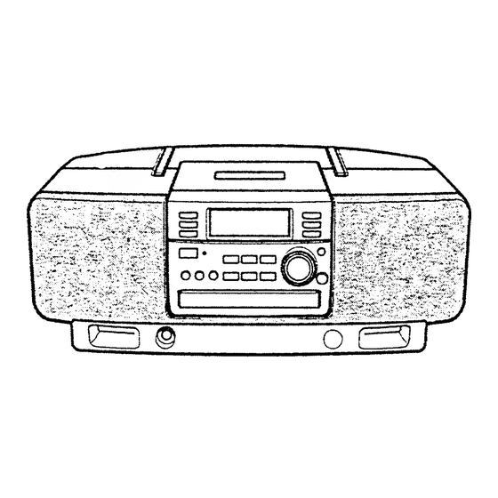
Aiwa CSD-EL300 Service Manual
Hide thumbs
Also See for CSD-EL300:
- Operating instructions manual (44 pages) ,
- Service manual (35 pages) ,
- Service manual (35 pages)
Table of Contents
Advertisement
Quick Links
QQ
3 7 63 1515 0
SERVICE MANUAL
TE
L 13942296513
COMPACT DISC STEREO RADIO
CASSETTE RECORDER
This Service Manual is the "Revision Publishing" and replaces "Simple Manual"
CSD-EL300 (S/M Code No. 09-003-344-1T1)
www
.
http://www.xiaoyu163.com
x
ao
u163
y
i
S/M Code No. 09-003-344-1R1
http://www.xiaoyu163.com
CSD-EL300
2 9
8
Q Q
3
6 7
1 3
1 5
BASIC TAPE MECHANISM : 2ZM-1YR7NC
BASIC CD MECHANISM : 3ZG-3 E2NC
co
.
K(S) EZ(S)
9 4
2 8
0 5
8
2 9
9 4
2 8
m
9 9
9 9
Advertisement
Table of Contents

Related Manuals for Aiwa CSD-EL300


Summary of Contents for Aiwa CSD-EL300
- Page 1 L 13942296513 COMPACT DISC STEREO RADIO BASIC TAPE MECHANISM : 2ZM-1YR7NC CASSETTE RECORDER BASIC CD MECHANISM : 3ZG-3 E2NC This Service Manual is the “Revision Publishing” and replaces “Simple Manual” CSD-EL300 (S/M Code No. 09-003-344-1T1) u163 S/M Code No. 09-003-344-1R1 http://www.xiaoyu163.com...
-
Page 2: Specifications
http://www.xiaoyu163.com SPECIFICATIONS 3 7 63 1515 0 L 13942296513 • Design and specifications are subject to change without notice ACCESSORIES/PACKAGE LIST REF. NO PART NO. KANRI DESCRIPTION 1 8A-CH2-906-010 IB,EZ(9L)FM<EZS> 1 8A-CH2-905-010 IB,K(E)FM<KS> 2 87-050-076-010 AC CORD SET ASSY,E u163 3 87-099-726-010 PLUG,ADPTR CONV(K)<KS>... -
Page 3: Protection Of Eyes From Laser Beam During Servicing
http://www.xiaoyu163.com PROTECTION OF EYES FROM LASER BEAM DURING SERVICING This set employs laser. Therefore, be sure to follow carefully the CAUTION 3 7 63 1515 0 instructions below when servicing. Use of controls or adjustments or performance of procedures other than those specified herein may result in hazardous WARNING! radiation exposure. -
Page 4: Electrical Main Parts List
http://www.xiaoyu163.com ELECTRICAL MAIN PARTS LIST 3 7 63 1515 0 REF. NO PART NO. KANRI DESCRIPTION REF. NO PART NO. KANRI DESCRIPTION C233 87-010-546-080 CAP, ELECT 0.33-50V C234 87-010-546-080 CAP, ELECT 0.33-50V 87-A21-550-010 IC,TA2149N C235 87-018-209-080 CAP, CER 0.1-50V 87-A21-185-040 C-IC,LC72121M C236 87-018-209-080... - Page 5 http://www.xiaoyu163.com 3 7 63 1515 0 REF. NO PART NO. KANRI DESCRIPTION REF. NO PART NO. KANRI DESCRIPTION C513 87-018-134-080 CAPACITOR,TC-U 0.01-16 C470 87-010-544-080 CAP, ELECT 0.1-50V C514 87-010-248-080 CAP, ELECT 220-10V C475 87-018-134-080 CAPACITOR,TC-U 0.01-16 C520 87-010-384-080 CAP, ELECT 100-25V C476 87-A10-102-080 CAP,E 1000-10 REA...
- Page 6 http://www.xiaoyu163.com 3 7 63 1515 0 REF. NO PART NO. KANRI DESCRIPTION REF. NO PART NO. KANRI DESCRIPTION 87-010-178-080 CHIP CAP 1000P C625 87-010-322-080 C-CAP,S 100P-50 CH 87-010-178-080 CHIP CAP 1000P C626 87-010-197-080 CAP, CHIP 0.01 DM 87-010-178-080 CHIP CAP 1000P C627 87-010-196-080 CHIP CAPACITOR,0.1-25...
-
Page 7: Chip Resistor Part Code
http://www.xiaoyu163.com 3 7 63 1515 0 • Regarding connectors, they are not stocked as they are not the initial order items. The connectors are available after they are supplied from connector manufacturers upon the order is received. CHIP RESISTOR PART CODE Chip Resistor Part Coding Figure Resistor Code... - Page 8 http://www.xiaoyu163.com LCD DISPLAY LCD, AIW4213 3 7 63 1515 0 L 13942296513 u163 http://www.xiaoyu163.com...
- Page 9 http://www.xiaoyu163.com SCHEMATIC DIAGRAM-1 (MAIN) 3 7 6 3 1 5 1 5 0 1 3 9 4 2 2 9 6 5 1 3 K/EZ 230V 50Hz w w w u 1 6 3 http://www.xiaoyu163.com...
- Page 10 http://www.xiaoyu163.com SCHEMATIC DIAGRAM-2 (CD MAIN) 3 7 6 3 1 5 1 5 0 1 3 9 4 2 2 9 6 5 1 3 w w w u 1 6 3 http://www.xiaoyu163.com...
- Page 11 http://www.xiaoyu163.com WIRING-1 (MAIN/CD MAIN) 3 7 6 3 1 5 1 5 0 1 3 9 4 2 2 9 6 5 1 3 w w w u 1 6 3 http://www.xiaoyu163.com...
- Page 12 http://www.xiaoyu163.com WIRING-2 (PWR/BATT) WIRING-3 (TU) 3 7 6 3 1 5 1 5 0 K/EZ: 230V/50Hz 1 3 9 4 2 2 9 6 5 1 3 w w w u 1 6 3 http://www.xiaoyu163.com...
- Page 13 http://www.xiaoyu163.com SCHEMATIC DIAGRAM-3 (TU) 3 7 6 3 1 5 1 5 0 1 3 9 4 2 2 9 6 5 1 3 0.015 R034 KS: 15k w w w EZS: 27k u 1 6 3 http://www.xiaoyu163.com...
- Page 14 http://www.xiaoyu163.com SCHEMATIC DIAGRAM-4 (FRONT) 3 7 6 3 1 5 1 5 0 1 3 9 4 2 2 9 6 5 1 3 w w w u 1 6 3 http://www.xiaoyu163.com...
- Page 15 http://www.xiaoyu163.com WIRING-4 (FRONT) 3 7 6 3 1 5 1 5 0 1 3 9 4 2 2 9 6 5 1 3 w w w u 1 6 3 http://www.xiaoyu163.com...
-
Page 16: Electrical Adjustment
http://www.xiaoyu163.com ELECTRICAL ADJUSTMENT < TUNER SECTION > < DECK SECTION > 3 7 6 3 1 5 1 5 0 MAIN C.B 1. MW IF Adjustment 8. Bias frequency Adjustment L007 ............... 450kHz L331 .............. 75Hz±500Hz 2. MW VT Adjustment 9. - Page 17 http://www.xiaoyu163.com IC BLOCK DIAGRAM IC, TA2149N 3 7 63 1515 0 L 13942296513 IC, LC72121M u163 http://www.xiaoyu163.com...
- Page 18 http://www.xiaoyu163.com IC, M61500FP 3 7 63 1515 0 INA1 INA2 Mono.SW INB1 INB2 INC1 INC2 MUTE IND1 IND2 INE1 INE2 Treble Treble boost boost TONEH1 TONEH2 TONEL1 TONEL2 Bass Bass boost boost OUT1 OUT2 Control logic CONT L 13942296513 IC, BU4094BCF u163 http://www.xiaoyu163.com...
- Page 19 http://www.xiaoyu163.com IC, LA6541D 3 7 63 1515 0 L 13942296513 u163 http://www.xiaoyu163.com...
- Page 20 http://www.xiaoyu163.com IC DESCRIPTION IC, LA9241ML 3 7 63 1515 0 Pin No. Pin Name Description Pin to which external pickup photo diode is connected. RF signal is created by adding FIN2 with the FIN1 pin signal. FE signal is created by subtracting from the FIN1 pin signal. FIN1 Pin to which external pickup photo diode is connected.
- Page 21 http://www.xiaoyu163.com 3 7 63 1515 0 Pin No. Pin Name Description Pin from which TES signal is output to DSP. “High Frequency Level” is used to judge whether the main beam position is on top of bit or on top of mirror. SLOF Sled servo off control input pin.
- Page 22 http://www.xiaoyu163.com IC, LC78622ED 3 7 63 1515 0 Pin No. Pin Name Description DEFI Defect sense signal (DEF) input pin. (Connect to 0V when not used). Test signal input pin with built-in pull-down resistor. Be sure to connect to 0V. Phase comparator output pin to control external VCO.
- Page 23 http://www.xiaoyu163.com 3 7 63 1515 0 Pin No. Pin Name Description XVDD — Crystal oscillator power supply pin. XOUT Pin to which external 16.9344 MHz crystal oscillator is connected. XVSS — Crystal oscillator GND pin. Be sure to connect to 0V. SBSY Subcode block sync signal output pin.
- Page 24 http://www.xiaoyu163.com IC, LC867132V-5P07 3 7 63 1515 0 Pin No. Pin Name Description O-RMC/CE CD read/write control output. O-DATA Data output to sound processor IC (M62495FP). O-CLK Clock output to sound processor IC (M62495FP). — Not Connected. O-CLK SFT Clock shift output of the microcomputer. I-HOLD Hold status detection.
- Page 25 http://www.xiaoyu163.com 3 7 63 1515 0 Pin No. Pin Name Description O-CD LED LED ON/OFF control output for CD functions. O-TU LED LED ON/OFF control output for TU functions. O-TA LED (NC) LED ON/OFF control output for TAPE functions. (Not Connected) O-ROCK LED LED ON/OFF control output for ROCK.
-
Page 26: Mechanical Parts List
http://www.xiaoyu163.com MECHANICAL PARTS LIST 1/1 3 7 63 1515 0 REF. NO PART NO. KANRI DESCRIPTION REF. NO PART NO. KANRI DESCRIPTION 1 8A-CH2-016-010 LENS,RC 31 88-CD5-203-010 HLDR,LOCK 2N 2 8A-CH2-012-010 COVER, FR 32 8A-CH2-621-010 FF-CABLE,16P 1.0 3 8A-CH2-030-010 FRAME, NET ASSY 33 8A-CH2-622-010 FF-CABLE,5P 1.25 4 8A-CH2-024-010... -
Page 27: Mechanical Exploded View
http://www.xiaoyu163.com MECHANICAL EXPLODED VIEW 1/1 3 7 6 3 1 5 1 5 0 2ZM-1 P.C.B SH,DISP CHAS,CENTER P.C.B 29 30 3ZG-3 HT-SINK 1 3 9 4 2 2 9 6 5 1 3 P.C.B P.C.B P.C.B P.C.B w w w u 1 6 3 http://www.xiaoyu163.com... -
Page 28: Tape Mechanism Exploded View
http://www.xiaoyu163.com TAPE MECHANISM EXPLODED VIEW 1/1 3 7 6 3 1 5 1 5 0 DECK C.B SOL2 1 3 9 4 2 2 9 6 5 1 3 RELAY C.B HLDR WIRE 3 w w w u 1 6 3 http://www.xiaoyu163.com... -
Page 29: Tape Mechanism Parts List
http://www.xiaoyu163.com TAPE MECHANISM PARTS LIST 1/1 3 7 63 1515 0 REF. NO PART NO. KANRI DESCRIPTION REF. NO PART NO. KANRI DESCRIPTION 1 82-ZM1-327-210 CHAS ASSY,RN 33 82-ZM1-227-210 LVR,TRIG 2 82-ZM1-258-010 SPR-T,PINCH L 34 82-ZM1-224-410 LVR,FR 3 82-ZM1-341-010 LVR ASSY,PINCH L 2 35 86-ZM4-201-010 SPR-E,TRIG 3 4 82-ZM1-295-310... -
Page 30: Cd Mechanism Exploded View
http://www.xiaoyu163.com CD MECHANISM EXPLODED VIEW 1/1 3 7 63 1515 0 CUSH-G, MAIN A CUSH-G, MAIN A 3ZG2 L 13942296513 MOTOR-2 C.B u163 http://www.xiaoyu163.com... - Page 31 http://www.xiaoyu163.com CD MECHANISM PARTS LIST 1/1 3 7 63 1515 0 REF. NO PART NO. KANRI DESCRIPTION REF. NO PART NO. KANRI DESCRIPTION 1 83-ZG3-224-310 HLDR,M2 16 83-ZG3-211-010 PLATE,DISC 2 83-ZG3-228-610 CHAS,L6 17 81-ZG1-254-010 S-SCEW,MECH HLDR 3 83-ZG3-208-010 PULLEY,MOTOR A 87-067-945-110 VFT2+3-12(F10) 4 83-ZG3-213-010 LVR,SW...
-
Page 32: Spring Application Position
http://www.xiaoyu163.com SPRING APPLICATION POSITION 3 7 63 1515 0 82-ZM1-257-010 82-ZM1-218-010 SPR-T,CAS SPR-E,HB 82-ZM1-285-410 82-ZM1-244-010 SPR-C,BT L SPR-C,BT 82-ZM3-323-010 SPR-T,LINK 82-ZM1-259-110 SPR-T,PINCH R 82-ZM1-258-110 SPR-T,PINCH L L 13942296513 82-ZM1-269-010 82-ZM1-214-010 82-ZM1-213-010 SPR-T,BRG SPR-T,DIR SPR-T,HEAD 82-ZM1-322-010 SPR-T,FR 60 86-ZM4-201-010 SPR-E,TRIG 3 82-ZM1-255-310 SPR-E,LER DIR u163... -
Page 33: Mechanical Section
http://www.xiaoyu163.com REFERENCE NAME LIST ELECTRICAL SECTION MECHANICAL SECTION 3 7 63 1515 0 DESCRIPTION REFERENCE NAME DESCRIPTION REFERENCE NAME ANTENNAS ADHESHIVE SHEET ADHESHIVE CHIP AZIMUTH C-CAP CAP, CHIP BAR-ANT BAR-ANTENNA C-CAP TN CAP, CHIP TANTALUM BATTERY C-COIL COIL, CHIP BATT BATTERY C-DI DIODE, CHIP... - Page 34 http://www.xiaoyu163.com 3 7 63 1515 0 L 13942296513 u163 2–11, IKENOHATA 1–CHOME, TAITO-KU, TOKYO 110, JAPAN TEL:03 (3827) 3111 737004 Printed in Singapore http://www.xiaoyu163.com...
Need help?
Do you have a question about the CSD-EL300 and is the answer not in the manual?
Questions and answers