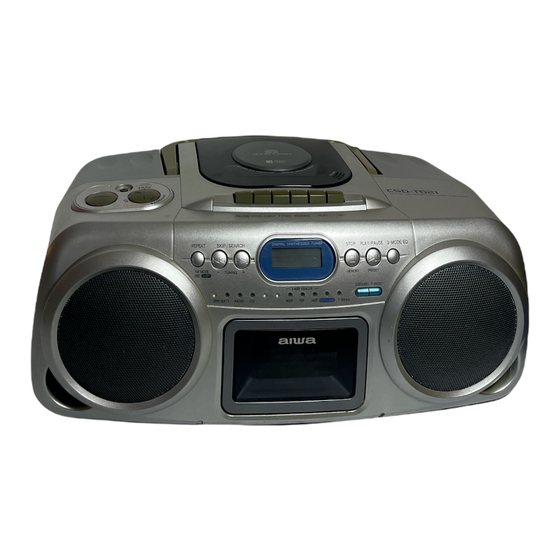
Aiwa CSD-TD21 Service Manual
Compact disc/stereo cassette recorder
Hide thumbs
Also See for CSD-TD21:
- Service manual (32 pages) ,
- Operating instructions manual (9 pages) ,
- Service manual (10 pages)
Table of Contents
Advertisement
Quick Links
All manuals and user guides at all-guides.com
CSD-TD21
HE
SERVICE MANUAL
COMPACT DISC /
BASIC TAPE MECHANISM : ZZM-1 AR2NC
STEREO CASSETTE RECORDER
BASIC CD MECHANISM : DA11T3C
• This Service Manual is the "Revision Publishing" and replaces "Simple Manual",
(S/M Code No. 09-006-426-7T2).
S/M Code No. 09-006-426-7R2
Advertisement
Table of Contents

Related Manuals for Aiwa CSD-TD21


Summary of Contents for Aiwa CSD-TD21
- Page 1 All manuals and user guides at all-guides.com CSD-TD21 SERVICE MANUAL COMPACT DISC / BASIC TAPE MECHANISM : ZZM-1 AR2NC STEREO CASSETTE RECORDER BASIC CD MECHANISM : DA11T3C • This Service Manual is the "Revision Publishing" and replaces "Simple Manual", (S/M Code No. 09-006-426-7T2).
-
Page 2: Specifications
All manuals and user guides at all-guides.com SPECIFICATIONS Tuner section General Frequency range Speaker 100 mm cone type (2) FM : 87.5 MHz - 108.0 MHz 60 mm cone type (2) Antenna : Rod antenna Output Headphones jack (stereo mini-jack) AM : 531/530 kHz - 1,602/1,710 kHz Power output... -
Page 3: Protection Of Eyes From Laser Beam During Servicing
All manuals and user guides at all-guides.com PROTECTION OF EYES FROM LASER BEAM DURING SERVICING This set employs laser. Therefore, be sure to follow carefully the CAUTION instructions below when servicing. Use of controls or adjustments or performance of procedures other than those specified herein may result in hazardous WARNING! radiation exposure. -
Page 4: Electrical Main Parts List
All manuals and user guides at all-guides.com ELECTRICAL MAIN PARTS LIST REF. NO. PART NO. KANRI DESCRIPTION REF. NO. PART NO. KANRI DESCRIPTION C807 87-010-405-080 CAP, ELECT 10-50V C808 87-010-405-080 CAP, ELECT 10-50V 87-A21-550-010 IC,TA2149N C809 87-010-401-080 CAP, ELECT 1-50V 87-A21-185-040 C-IC,LC72121M C810... - Page 5 All manuals and user guides at all-guides.com REF. NO. PART NO. KANRI DESCRIPTION REF. NO. PART NO. KANRI DESCRIPTION C416 87-010-545-080 CAP, ELECT 0.22-50V CN202 8A-CH4-689-010 CONN,3P V 2.5 C417 87-012-157-080 C-CAP,S 330P-50 CH CN205 87-A60-109-010 CONN,2P V S2M-2W C418 87-010-213-080 C-CAP,S 0.015-25 B CN301...
- Page 6 All manuals and user guides at all-guides.com REF. NO. PART NO. KANRI DESCRIPTION REF. NO. PART NO. KANRI DESCRIPTION 87-010-197-080 CAP, CHIP 0.01 DM 87-A60-110-010 CONN,4P V S2M-4W 87-010-197-080 CAP, CHIP 0.01 DM 87-A40-616-070 VARI-CAP,SVC384(S/T) 87-010-197-080 CAP, CHIP 0.01 DM 87-A40-916-040 C-VARI-CAP,HVC202A 87-010-150-080...
-
Page 7: Chip Resistor Part Code
All manuals and user guides at all-guides.com CHIP RESISTOR PART CODE Chip Resistor Part Coding Figure Resistor Code Value of resistor Chip resistor Dimensions (mm) Wattage Type Tolerance Symbol Resistor Code Form 1/16W 1005 0.35 1/16W 1608 0.45 1/10W 2125 1.25 0.45 1/8W... - Page 8 All manuals and user guides at all-guides.com WIRING – 1 (MAIN / CD) – 8 –...
- Page 9 All manuals and user guides at all-guides.com SCHEMATIC DIAGRAM - 1 (MAIN / CD 1 / 2 / H.P. / BATT1 / BATT2) – 9 –...
- Page 10 All manuals and user guides at all-guides.com SCHEMATIC DIAGRAM - 2 (CD 2 / 2) – 10 –...
- Page 11 All manuals and user guides at all-guides.com WIRING – 2 (FRONT / H.P. / BATT1 / BATT2) – 11 –...
-
Page 12: Schematic Diagram - 3 (Front)
All manuals and user guides at all-guides.com SCHEMATIC DIAGRAM - 3 (FRONT) – 12 –... - Page 13 All manuals and user guides at all-guides.com WIRING – 3 (TUNER) – 13 –...
-
Page 14: Schematic Diagram - 4 (Tuner)
All manuals and user guides at all-guides.com SCHEMATIC DIAGRAM - 4 (TUNER) – 14 –... - Page 15 All manuals and user guides at all-guides.com WIRING - 5 (MOTOR) H MOTOR C.B (SLED MOTOR) (INSIDE LIMIT SW) (SPINDLE MOTOR) – 15 –...
- Page 16 All manuals and user guides at all-guides.com LCD DISPLAY LCD, HLC7365 – 16 –...
- Page 17 All manuals and user guides at all-guides.com IC BLOCK DIAGRAM IC,M61509FP IC,LC72121M IC,M62495AFP – 17 –...
- Page 18 All manuals and user guides at all-guides.com IC,BA4560N IC,LA6541D IC,TA2149N – 18 –...
- Page 19 All manuals and user guides at all-guides.com IC DESCRIPTION IC, LC867132V-5P07 Pin No. Pin Name Description O-RWC / CE CD read/write control (TU CE). O-DATA Data output to LC72121M/M62495FP. O-CLK CLK output to LC72121M. Not used. O-CK SFT Clock shift output of the microcomputer. I-HOLD Hold status detection.
- Page 20 All manuals and user guides at all-guides.com VSS3 Connected to GND. 43~44 S12~S13 LCD segment output. 45~50 S16~S21 LCD segment output. 51~54 S22~S25 Not used. O-CD LED LED ON/OFF control output for CD functions. O-TU LED LED ON/OFF control output for TU functions. O-TA LED LED ON/OFF control output for TAPE functions.
- Page 21 All manuals and user guides at all-guides.com IC, LC78622ED Pin No. Pin Name Description DEFI Defect detection signal (DEF) input. Test input. A pull-down resistor is built in. Must be connected to 0V. External VCO control phase comparator output. VVSS –...
- Page 22 All manuals and user guides at all-guides.com Pin No. Pin Name Description LVSS – Left channel one-bit D/A converter ground. Must be connected to 0V. RVSS Right channel one-bit D/A converter ground. (Must be connected to 0V.) RCHO Right channel onr-bit D/A converter output. RVDD Right channel one-bit D/A converter power supply.
- Page 23 All manuals and user guides at all-guides.com IC, LA9241ML Pin No. Pin Name Description For the connection of the pickup photodiode. Addition to the FIN1 pin creates an RF FIN2 signal and subtraction from it create an EF signal. FIN1 For the connection of the pickup photodiode.
- Page 24 All manuals and user guides at all-guides.com Pin No. Pin Name Description The HFL (high frequency level) signal is used to judge whether the main beam is positioned on the pit or on the mirror. SLOF Sled servo off control input. CLV error signal input from the DSP.
- Page 25 All manuals and user guides at all-guides.com ADJUSTMENT <TUNER / DECK / CD> < TUNER SECTION > < DECK SECTION > 1. FM VT Adjustment 6. Tape Speed Adjustment Settings : • Test point : TP2(VT) Settings : • Test tape : TTA–100 •...
-
Page 26: Mechanical Exploded View
MECHANICAL EXPLODED VIEW 1 / 1 P.C.B P.C.B P.C.B P.C.B P.C.B GRILLE, GRILLE, FR L FR L P.C.B P.C.B P.C.B P.C.B P.C.B P.C.B P.C.B P.C.B P.C.B CHASS,TU ZZM-1 GRILLE, GRILLE, FR R FR R CSD-TD21/TD20 HSCC CSD-TD21 (FileName:EXP.EPS) (FileName:EXP.EPS) 12/6/21 (ACH-9) – 26 –... -
Page 27: Mechanical Part List
MECHANICAL PART LIST 1 / 1 REF. NO. PART NO. KANRI DESCRIPTION REF. NO. PART NO. KANRI DESCRIPTION 1 87-B00-010-010 BADGE,AIWA 30.5-5.2 S 2.5L 36 8A-CD9-005-010 CHAS,CD A 2 8A-CD9-009-010 WINDOW,CASS 37 8Z-CDB-169-010 PANEL,CD SANYO 3 8A-CD9-232-010 SPR-T,CASS 38 8A-CD9-231-010... -
Page 28: Tape Mechanism Exploded View
All manuals and user guides at all-guides.com TAPE MECHANISM EXPLODED VIEW 1 / 1 TERMINAL,LB1 – 28 –... -
Page 29: Tape Mechanism Parts List
All manuals and user guides at all-guides.com TAPE MECHANISM PARTS LIST 1 / 1 REF. NO. PART NO. KANRI DESCRIPTION REF. NO. PART NO. KANRI DESCRIPTION 1 8Z-ZM1-254-310 0E SPR-C,REEL R 31 87-A91-819-010 0E HEAD,EH 2NSS-2200 2 8Z-ZM1-225-110 0E GEAR,REEL R 32 8Z-ZM1-215-010 0E LEVER,REC LOCK 3 8Z-ZM1-253-210 0E SPR-C,AUTO SENSOR 33 87-A91-492-010 0E SW,LEAF MSW18560... -
Page 30: Cd Mechanism Exploded View
All manuals and user guides at all-guides.com CD MECHANISM EXPLODED VIEW 1 / 1 SHAFT,SLIDE SF-P101NR CHASSIS SPINDLE MOTOR C,B MOTOR(M1) CD MECHANISM PARTS LIST 1 / 1 REF. NO. PART NO. KANRI DESCRIPTION 1 S2-121-A28-400 COVER GEAR 2 S2-511-A21-000 GEAR MIDDLE 3 S2-511-A21-100 GEAR,DRIVE... - Page 31 All manuals and user guides at all-guides.com 2–11, IKENOHATA 1–CHOME, TAITO-KU, TOKYO 110, JAPAN TEL:03 (3827) 3111 9620450 0251431 Printed in Singapore...
Need help?
Do you have a question about the CSD-TD21 and is the answer not in the manual?
Questions and answers