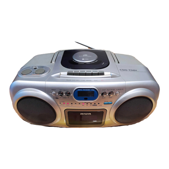
Aiwa CSD-TD61 Service Manual
Compact disc stereo radio cassette recorder
Hide thumbs
Also See for CSD-TD61:
- Operating instructions manual (9 pages) ,
- Service manual (31 pages) ,
- Service manual (32 pages)

Subscribe to Our Youtube Channel
Related Manuals for Aiwa CSD-TD61


Summary of Contents for Aiwa CSD-TD61
- Page 1 CSD-TD61 V(S) SERVICE MANUAL COMPACT DISC STEREO RADIO BASIC TAPE MECHANISM : ZZM-1AR2 CASSETTE RECORDER BASIC CD MECHANISM : DA11T3C MODEL CODE : 86HR8-0117(B) SIMPLE-2 S/M Code No. 09-003-343-9N2...
-
Page 2: Specifications
SPECIFICATIONS • Design and specifications are subject to change without notice ACCESSORIES/PACKAGE LIST REF. NO PART NO. KANRI DESCRIPTION 1 8A-CHK-907-010 IB,V(ER)B 2 8Z-CK4-962-010 RC UNIT,RC-ZAT04 (VS) 3 87-A80-081-010 AC CORD SET ASSY,EZ BLK... -
Page 3: Protection Of Eyes From Laser Beam During Servicing
PROTECTION OF EYES FROM LASER BEAM DURING SERVICING This set employs laser. Therefore, be sure to follow carefully the CAUTION instructions below when servicing. Use of controls or adjustments or performance of procedures other than those specified herein may result in hazardous WARNING! radiation exposure. -
Page 4: Electrical Main Parts List
ELECTRICAL MAIN PARTS LIST REF. NO PART NO. KANRI DESCRIPTION REF. NO PART NO. KANRI DESCRIPTION C324 87-010-260-080 CAP, ELECT 47-25V C325 87-010-405-080 CAP, ELECT 10-50V 87-A21-550-010 IC,TA2149N C401 87-010-403-080 CAP, ELECT 3.3-50V 87-A21-185-040 C-IC,LC72121M C402 87-010-197-080 CAP, CHIP 0.01 DM 87-A21-064-010 IC,LA4227 C403... - Page 5 REF. NO PART NO. KANRI DESCRIPTION REF. NO PART NO. KANRI DESCRIPTION C480 87-010-221-080 CAP, ELECT 470-10V 87-010-312-080 C-CAP,S 15P-50 CH C481 87-010-405-080 CAP, ELECT 10-50V 87-010-197-080 CAP, CHIP 0.01 DM C482 87-010-405-080 CAP, ELECT 10-50V 87-010-197-080 CAP, CHIP 0.01 DM C489 87-012-368-080 C-CAP,S 0.1-50 F...
- Page 6 REF. NO PART NO. KANRI DESCRIPTION REF. NO PART NO. KANRI DESCRIPTION C843 87-010-197-080 CAP, CHIP 0.01 DM LED607 88-CD6-630-010 LED,934ID RED C844 87-018-124-080 CAP, CER 270P-50V LED608 88-CD6-630-010 LED,934ID RED C845 87-010-178-080 CHIP CAP 1000P LED610 88-CD6-631-010 LED,934GD GRN C846 87-010-263-080 CAP, ELECT 100-10V...
-
Page 7: Lcd Display
LCD DISPLAY LCD, 7365 ZCH-4 • Regarding connectors, they are not stocked as they are not the initial order items. The connectors are available after they are supplied from connector manufacturers upon the order is received. CHIP RESISTOR PART CODE Chip Resistor Part Coding Figure Resistor Code... - Page 8 WIRING-1 (MAIN/TAPE) L203 L201...
- Page 9 WIRING-2 (HP/BATT/MOTOR) SP903 SP904 SP902 SP901 50Hz OTOR C.B (SLED MOTOR) (INSIDE LIMIT SW) (SPINDLE MOTOR)
- Page 10 SCHEMATIC DIAGRAM-1 (MAIN 1/2: TAPE) C211 0.15/16 C212 0.15/16 R255 2.2k D201 IN4148 C272 1000 C271 1000 D202 IN4148 BATT1 PT, E 2.5W HZ7A1L Q251 2SA933S 2.5A 491 50Hz IN4148 D203 IN4148 BATT2...
- Page 11 SCHEMATIC DIAGRAM-2 (MAIN 2/2) C495...
- Page 12 WIRING-3 (FRONT) FRONT C.B (CHIP PARTS) R616 C701 C702 C608 C605 R611 C620 R639 R627 C705 C706 R644 R619 R640 R618 R639 JR629 C710 C711 R633 C709 C708 C707 C614 R605 R606 FRONT C.B (INSERTED PARTS) TO MAIN C.B TO TAPE C.B CN201 CN403 NOTE C704...
- Page 13 SCHEMATIC DIAGRAM-3 (FRONT) TU V 1.5k 1.5k 1.8k...
- Page 14 SCHEMATIC DIAGRAM-4 (TUNER)
- Page 15 WIRING-4 (TUNER) L061 C061 D061 R061...
-
Page 16: Electrical Adjustment
ELECTRICAL ADJUSTMENT L003 (BAR-ANT) TU C.B TC001 L005 HP C.B L007 IC001 L004 J251 L006 TAPE C.B L801 (DECK MOTOR) -
Page 17: Tuner Section
< TUNER SECTION > 1. AM IF Adjustment L007 ............... 450kHz 2. AM VT Adjustment Settings: • Test point: C39+ • Adjustment location: L004 Method: Set to AM 999kHz adjust L004 so that the test point becomes 3.75V±50mV. 3. AM Tracking Adjustment L003 ............... - Page 18 IC BLOCK DIAGRAM IC, TA2149N IC, LC72121M...
- Page 19 IC, M61509FP INA1 INA2 Mono.SW INB1 INB2 INC1 INC2 MUTE IND1 IND2 INE1 INE2 Treble Treble boost boost TONEH1 TONEH2 TONEL1 TONEL2 Bass Bass boost boost OUT1 OUT2 Control logic CONT IC, LA4227...
- Page 20 IC, LA6541D IC, LA4600 STANDBY SW STANDBY SW R IN OUTPUT PRE DRIVE INPUT AMP R OUT RN11 TSD PROTECTER RN12 OUTPUT PRE DRIVE L OUT INPUT AMP L IN NOISE REPLE FILTER PREVENTION FILTER...
- Page 21 IC, BA4560N...
- Page 22 IC DESCRIPTION IC, LA9241ML Pin No. Pin Name Description Pin to which external pickup photo diode is connected. RF signal is created by adding FIN2 with the FIN1 pin signal. FE signal is created by subtracting from the FIN1 pin signal. FIN1 Pin to which external pickup photo diode is connected.
- Page 23 Pin No. Pin Name Description Pin from which TES signal is output to DSP. “High Frequency Level” is used to judge whether the main beam position is on top of bit or on top of mirror. SLOF Sled servo off control input pin. 39, 40 CV–, CV+ CLV error signal input pin from DSP.
- Page 24 IC, LC78622ED Pin No. Pin Name Description DEFI Defect sense signal (DEF) input pin. (Connect to 0V when not used). Test signal input pin with built-in pull-down resistor. Be sure to connect to 0V. Phase comparator output pin to control external VCO. VVSS —...
- Page 25 Pin No. Pin Name Description XVDD — Crystal oscillator power supply pin. XOUT Pin to which external 16.9344 MHz crystal oscillator is connected. XVSS — Crystal oscillator GND pin. Be sure to connect to 0V. SBSY Subcode block sync signal output pin. EFLG C1, C2, single and dual correction monitoring pin.
- Page 26 IC, LC867132V-5P07 Pin No. Pin Name Description O-RMC/CE CD read/write control output. O-DATA Data output to sound processor IC (M62495FP). O-CLK Clock output to sound processor IC (M62495FP). — Not Connected. O-CLK SFT Clock shift output of the microcomputer. I-HOLD Hold status detection.
- Page 27 Pin No. Pin Name Description O-CD LED LED ON/OFF control output for CD functions. O-TU LED LED ON/OFF control output for TU functions. O-TA LED (NC) LED ON/OFF control output for TAPE functions. (Not Connected) O-ROCK LED LED ON/OFF control output for ROCK. O-POP LED LED ON/OFF control output for POP.
-
Page 28: Mechanical Parts List
MECHANICAL PARTS LIST 1/1 REF. NO PART NO. KANRI DESCRIPTION REF. NO PART NO. KANRI DESCRIPTION 1 87-B00-010-010 BADGE,AIWA 30.5-5.2 S 2.5L 41 8A-CD8-603-010 PT,E 2.5W 2 8A-CD9-009-010 WINDOW,CASS 42 8A-CH4-209-010 HLDR,PT 3 8A-CD9-232-010 SPR-T,CASS 43 8A-CD9-012-010 HANDL,GRIP 4 8A-CD9-008-010... -
Page 29: Mechanical Exploded View
MECHANICAL EXPLODED VIEW 1/1 CUSHION, P.C.B P.C.B CUSHION, CUSHION, CUSHION, CDA P.C.B P.C.B GRILLE, FR L P.C.B P.C.B P.C.B ZZM-1 P.C.B P.C.B BAR-ANT CHAS,TU A GRILLE, FR R... -
Page 30: Tape Mechanism Exploded View
TAPE MECHANISM EXPLODED VIEW 1/1 TAPE MECHANISM PARTS LIST 1/1 REF. NO PART NO. KANRI DESCRIPTION REF. NO PART NO. KANRI DESCRIPTION 1 8Z-ZM1-254-310 SPR-C,REEL R 31 87-A91-819-010 HEAD,EH 2NSS-2200 2 8Z-ZM1-225-110 GEAR,REEL R 32 8Z-ZM1-215-010 LEVER,REC LOCK 3 8Z-ZM1-253-210 SPR-C,AUTO SENSOR 33 87-A91-492-010 SW,LEAF MSW18560... -
Page 31: Cd Mechanism Exploded View
CD MECHANISM EXPLODED VIEW 1/1 SHAFT,SLIDE SF-P101NR CHASSIS SPINDLE MOTOR C,B MOTOR(M3) CD MECHANISM PARTS LIST 1/1 REF. NO PART NO. KANRI DESCRIPTION 1 S2-121-A28-400 COVER GEAR 2 S2-511-A21-000 GEAR MIDDLE 3 S2-511-A21-100 GEAR,DRIVE A S1-PN2-03R-OSE SCR PAN PCS 2-3 B 87-261-073-410 SCR S-TPG FLT 2.6-6 ALL M8-ZZK-E90-070... - Page 32 2–11, IKENOHATA 1–CHOME, TAITO-KU, TOKYO 110-8710, JAPAN TEL:03 (3827) 3111 737004 Printed in Singapore...
Need help?
Do you have a question about the CSD-TD61 and is the answer not in the manual?
Questions and answers