Sony CDP-CX333ES Service Manual
Hide thumbs
Also See for CDP-CX333ES:
- Operating instructions manual (35 pages) ,
- Limited warranty (1 page) ,
- Operating instructions manual (20 pages)
Table of Contents
Advertisement
Advertisement
Table of Contents

Subscribe to Our Youtube Channel
Related Manuals for Sony CDP-CX333ES


Summary of Contents for Sony CDP-CX333ES
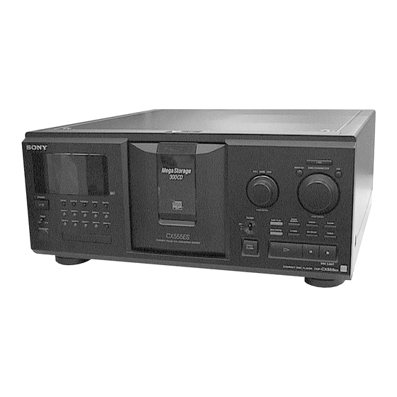
- Page 1 CDP-CX333ES/CX555ES SERVICE MANUAL US Model Canadian Model Photo: CX555ES Model Name Using Similar Mechanism CDP-CX300 CD Mechanism Type CDM54-KIBD35B Base Unit Type KSM-213BFN/C2NP Optical Pick-up Type KSS-213B/C2N SPECIFICATIONS 555ES 333ES COMPACT DISC PLAYER MICROFILM...
-
Page 2: Table Of Contents
OPERATION. REPLACE THESE COMPONENTS WITH DE FONCTIONNEMENT. NE REMPLACER CES COM- SONY PARTS WHOSE PART NUMBERS APPEAR AS POSANTS QUE PAR DES PIÈCES SONY DONT LES SHOWN IN THIS MANUAL OR IN SUPPLEMENTS PUB- NUMÉROS SONT DONNÉS DANS CE MANUEL OU LISHED BY SONY. - Page 3 SAFETY CHECK-OUT NOTES ON HANDLING THE OPTICAL PICK-UP After correcting the original service problem, perform the follow- BLOCK OR BASE UNIT ing safety check before releasing the set to the customer: The laser diode in the optical pick-up block may suffer electro- Check the antenna terminals, metal trim, “metallized”...
- Page 4 CD-TEXT TEST DISC This unit is able to display the TEXT data (character information) written in the CD on its fluorescent indicator tube. The CD-TEXT TEST DISC (TGCS-313:J-2501-126-A) is used for checking the display. To check, perform the following procedure. Checking Method: 1.
- Page 5 Table 2: CD-TEXT TEST DISC Recorded Contents and Display (In this unit, some special characters cannot be displayed. This is no a fault.) TRACK Recorded Contents Displayed Contents ! ” # $ % & ´ (21h to 27h) 1kHz 0dB L&R N All the same + , –...
- Page 6 PRECAUTIONS AT SERVICING Handling of wires (loading motor). (Fig. 3) Destruction of IC due Cleaning of optical to shortcircuit. (Fig. 4) pick-up. (Fig. 2) Alignment of door drive gear phase. (Fig. 1) ALIGNMENT OF DOOR DRIVE GEAR CLEANING OF OPTICAL PICK-UP (Fig. 2) PHASE WITH DOOR (CD) (Fig.
- Page 7 HANDLING OF WIRES (LOADING MOTOR) (Fig. 3) MAIN board loading motor lead pin When assembling this set after service, let the wires connected from loading motor to MAIN board through a notch of JACK board JACK board and clamp with a lead pin so that they are not caught in by the gear (table).
-
Page 8: General
SECTION 2 GENERAL • LOCATION OF CONTROLS 1 STANDBY indicator 2 1/u button – Front Panel – 3 TIMER switch 4 KEYBOARD jack 579 !¡ !£ !∞ !¶ !ª 5 CONTINUE button !™ !¢ !§ !• @º@¡@™ 6 GROUP1 button and indicator 7 SHUFFLE button 8 GROUP2 button and indicator @£... -
Page 9: Disassembly
SECTION 3 DISASSEMBLY Note: Follow the disassembly procedure in the numerical order given. FRONT PANEL ASSEMBLY 1 flat wire (CN502) 3 three screws (BVTP3 × 8) 4 claw 2 connector (CNP203) 5 front panel assembly 4 claw 6 cover 3 three screws (chassis) (BVTP3 ×... - Page 10 BASE (DOOR, GEAR) ASSEMBLY AND COVER (P. T.) 4 Remove the door assembly in arrow B 6 base (door.gear) !º two screws (BVTP3 × 8) direction. assembly 1 connector 7 three screws (CN509) (BVTP3 × 8) 2 two screws (BVTP3 × 8) 3 cover (front) 9 bracket...
- Page 11 MAIN BOARD AND BACK PANEL SECTION 6 four screws 2 two connectors (3 × 8) (CN503, 507) 1 flat wire (CN501) 4 MAIN board 7 back panel section 3 two screws (BVTP3 × 8) 6 three screws (3 × 8) 5 connector (CN991) 3 two screws...
-
Page 12: Service Mode
SECTION 4 SERVICE MODE SPECIAL FUNCTION This unit is provided with several service modes. Details are shown in the following table. Mode name Power supply state Button operation Remarks [CLEAR] [ ] ALL ERASE Note 1 [GROUP 1] [ OPEN/CLOSE] [+100] AGING MODE §... - Page 13 Special Aging Mode Functions Aging Procedure [ OPEN/CLOSE] The aging mode is provided with the following convenient func- 1. Turn ON the power of the unit. Press the § tions and open the front cover. [COMMAND MODE] [CD1] • Disc setting mode (*1) 2.
- Page 14 LOADING AGING MODE TABLE ROTATION MODE • This mode is used for repeating loading operations continuously. • This mode is used for electrical adjustments. Refer to the sec- • Aging will be performed continuously unless an error occurs. tion on Electrical Adjustments. •...
- Page 15 MECHANISM ADJUSTMENT MODE • This mode is used for mechanism adjustments. Refer to the sec- tion on Mechanism Adjustments. SHIPMENT MODE • This mode is used for setting the unit to the shipment state. Do not execute it without a proper reason as it erases the memory of the title memo recorded by the customer.
-
Page 16: Test Mode
SECTION 5 TEST MODE 5-1. ADJ MODE 5-2. KEY AND DISPLAY CHECK MODE To set this mode, connect the ^º pin of IC501 (AFADJ) on the 1. Turn ON the power of the unit, set disc to disc table, and per- form chucking. -
Page 17: Mechanical Adjustments
SECTION 6 MECHANICAL ADJUSTMENTS POP UP MECHANISM ADJUSTMENT [GROUP 4] [ ] 1. With the power ON, while pressing the · GROUP 1 [+100] GROUP 2 buttons, press the button to enter the mechanism ad- justment mode. GROUP 4 [GROUP 1] 2. Press the button to operate the loading mecha- nism, and continue pressing until the disc table locks. - Page 18 SENSOR ADJUSTMENT [GROUP 4] [ ] · 1. With the power ON, while pressing the GROUP 1 [+100] buttons, press the button to enter the mechanism ad- PAUSE button justment mode. GROUP 4 [GROUP 1] 2. Press the button to operate the loading mecha- PLAY button nism, and continue pressing until the disc table locks.
-
Page 19: Electrical Adjustment
SECTION 7 ELECTRICAL ADJUSTMENT Note: A clear RF signal waveform means that the shape “≈” can be clearly 1. CD Block is basically designed to operate without adjustment. distinguished at the center of the waveform. Therefore, check each item in order given. 2. - Page 20 [DISC/CHARACTER] Disc In Detect Sensor Adjustment 5. Rotate the knob in the counterclock- Be sure to perform this adjustment after sensor adjustment in wise direction and the disc table starts to rotate in the same MECHANICAL ADJUSTMENT. direction. Check that the waveform at this time is the same as that in step 4.
-
Page 21: Diagrams
CDP-CX333ES/CX555ES SECTION 8 DIAGRAMS 8-1. BLOCK DIAGMRAM – BD Section – FILTER OPTICAL PICK-UP (KSS-213B/C2N) IC103 RF AMP,FOCUS/TRACKING ERROR AMP IC101 LASER DIGITAL SIGNAL PROCESSOR,DIGITAL SERVO PROCESSOR,DIGITAL FILTER,D/A CONVERTER DIODE POWER 53 55 APC LD DIGITAL IC901 DOUT DIGITAL AUTOMATIC... -
Page 22: Block Diagram - Main Section
CDP-CX333ES/CX555ES 8-2. BLOCK DIAGRAM – MAIN Section – J903 2ND CD IN D/A CONVERTER S MUTE CURRENT PULS IC201 Q338 IC202 IC302(2/2) L1(+) IOL+ BUFFER LRCKI IN1+L LINE LRCK (+)BUF MIX AMP IC301(1/2) DATAI NOISE IC302(1/2) LINE OUT ADATA SHAPER L1(–) -
Page 23: Note For Printed Wiring Boards And Schematic Diagrams
8-3. NOTE FOR PRINTED WIRING BOARDS AND SCHEMATIC DIAGRAMS • Circuit Boards Location Note on Printed Wiring Board: Note on Schematic Diagram: • X : parts extracted from the component side. • All capacitors are in µF unless otherwise noted. pF: µµF •... -
Page 24: Printed Wiring Board - Bd Board
CDP-CX333ES/CX555ES 8-4. PRINTED WIRING BOARD – BD Board – • See page 23 for Circuit Boards Location. (Page 27) -
Page 25: Schematic Diagram - Bd Board
CDP-CX333ES/CX555ES 8-5. SCHEMATIC DIAGRAM – BD Board – • See page 42 for Waveforms. • See page 44 for IC Block Diagrams. (Page 29) The components identified by mark ! or dotted Les composants identifiés par une marque ! sont line with mark ! are critical for safety. -
Page 26: Printed Wiring Board - Main Board
CDP-CX333ES/CX555ES 8-6. PRINTED WIRING BOARD – MAIN Board – • See page 23 for Circuit Boards Location. - Page 27 CDP-CX333ES/CX555ES (Page 40) (Page 40) (Page 38) (Page 38) (Page 36) (Page 32) (Page (Page 24) (Page 40) (Page 38) (Page 31) (Page 31) (Page 38) • Semiconductor Location Ref. No. Location Ref. No. Location Ref. No. Location Ref. No. Location Ref.
-
Page 28: Schematic Diagram - Main Board (1/3)
CDP-CX333ES/CX555ES 8-7. SCHEMATIC DIAGRAM – MAIN Board (1/3) – • See page 43 for Waveforms. • See page 47 for IC Block Diagrams. (Page 39) (Page 39) (Page 39) (Page 39) (Page 37) (Page 39) (Page 33) (Page 30) (Page 30) -
Page 29: Schematic Diagram - Main Board (2/3)
CDP-CX333ES/CX555ES 8-8. SCHEMATIC DIAGRAM – MAIN Board (2/3) – • See page 42 for Waveforms. • See page 46 for IC Block Diagrams. (Page 25) (Page 31) (Page 30) -
Page 30: Schematic Diagram - Main Board (3/3)
CDP-CX333ES/CX555ES 8-9. SCHEMATIC DIAGRAM – MAIN Board (3/3) – • See page 47 for IC Block Diagrams. (Page 29) (Page 28) (Page 28) (Page 28) (Page 31) (Page 28) (Page 41) (Page 41) (Page 41) -
Page 31: Printed Wiring Board - Jack Board
CDP-CX333ES/CX555ES 8-10. PRINTED WIRING BOARD – JACK Board – • See page 23 for Circuit Boards Location. 8-11. SCHEMATIC DIAGRAM – JACK Board – (Page 29) A1 II (Page 30) (Page 27) (Page 27) -
Page 32: Printed Wiring Board - Display Board
CDP-CX333ES/CX555ES 8-12. PRINTED WIRING BOARD – DISPLAY Board – • See page 23 for Circuit Boards Location. (Page 34) (Page 27) • Semiconductor Location Ref. No. Location D701 D702 D703 D704 D705 D706 D707 D708 D709 D710 D771 D772 D773... -
Page 33: Schematic Diagram - Display Board
CDP-CX333ES/CX555ES 8-13. SCHEMATIC DIAGRAM – DISPLAY Board – • See page 43 for Waveforms. • See page 48 for IC Block Diagrams. (Page 35) (Page 39) (Page 28) -
Page 34: Printed Wiring Board - Jog Board
CDP-CX333ES/CX555ES 8-14. PRINTED WIRING BOARD – JOG Board – • See page 23 for Circuit Boards Location. • Semiconductor Location Ref. No. Location D711 D712 D713 D714 (Page 32) D715 D716 S706 FILTER S743-745, S751-756, S761-766... -
Page 35: Schematic Diagram - Jog Board
CDP-CX333ES/CX555ES 8-15. SCHEMATIC DIAGRAM – JOG Board – (Page 33) -
Page 36: Printed Wiring Boards - D.sensor (In)/D.sensor (Out)/Sensor (T) Boards
CDP-CX333ES/CX555ES 8-16. PRINTED WIRING BOARDS – D.SENSOR (IN)/D.SENSOR (OUT)/SENSOR (T) Boards – • See page 23 for Circuit Boards Location. D.SENSOR(IN) BOARD DISC IN DETECT SENSOR D.SENSOR(OUT) BOARD DISC IN DETECT SENSOR SENSOR(T) BOARD TABLE POSITION SENSOR 1-4 (Page 27) -
Page 37: Schematic Diagram - D.sensor (In)/D.sensor (Out)/Sensor (T) Boards
CDP-CX333ES/CX555ES 8-17. SCHEMATIC DIAGRAM – D.SENSOR (IN)/D.SENSOR (OUT)/SENSOR (T) Boards – (Page 28) -
Page 38: Printed Wiring Boards - D.motor/D.switch/Key/Led/L.t.motor/L.switch (A)/L.switch (B) Boards
CDP-CX333ES/CX555ES 8-18. PRINTED WIRING BOARDS – D.MOTOR/D.SWITCH/KEY/LED/L.T.MOTOR/L.SWITCH (A)/L.SWITCH (B) Boards – • See page 23 for Circuit Boards Location. (Page 27) (CX333ES) (CX555ES) (Page 32) (Page 27) (CX555ES) (Page 27) D.SWITCH BOARD (DOOR OPEN/CLOSE) (DOOR OPEN/CLOSE) CLOSE OPEN CLOSE OPEN L.SWITCH(A) BOARD... -
Page 39: Schematic Diagram - D.motor/D.switch/ Key/Led/L.t.motor/L.switch (A)/ L.switch (B) Boards
CDP-CX333ES/CX555ES 8-19. SCHEMATIC DIAGRAM – D.MOTOR/D.SWITCH/KEY/LED/L.T.MOTOR/L.SWITCH (A)/L.SWITCH (B) Boards – (Page 28) (Page 33) (Page 28) (Page 28) (Page 28) (Page 28) -
Page 40: Printed Wiring Board - Power Board
CDP-CX333ES/CX555ES 8-20. PRINTED WIRING BOARD – POWER Board – • See page 23 for Circuit Boards Location. (Page 27) (Page 27) (Page 27) • Semiconductor Location Ref. No. Location Ref. No. Location D901 D930 D910 D931 D911 D932 D912 D933... -
Page 41: Schematic Diagram - Power Board
CDP-CX333ES/CX555ES 8-21. SCHEMATIC DIAGRAM – POWER Board – (Page 30) (Page 30) (Page 30) The components identified by mark ! or dotted Les composants identifiés par une marque ! sont line with mark ! are critical for safety. critiques pour la sécurité. Ne les remplacer que Replace only with part number specified. - Page 42 • Waveforms – BD Board – – MAIN Board – 6 IC101 ^¡ (LRCK) 1 IC101 @§ (MDP) 1 IC201 1 (INVO) 2.6 Vp-p 5.8 Vp-p 4 Vp-p 16.9344 MHz 7.9 µ s 22.7 µ s 2 IC101 #ª (FE) 7 IC101 ^™...
- Page 43 – DISPLAY Board – 6 IC201 $£, $¶ (256FSO, MCLKI) 1 IC701 #• (OSCO) 4.8 Vp-p 2.3 Vp-p 89 ns 492 ns 7 IC201 %¢ (128FSO) 2 IC701 %ª (OSCI) 4.7 Vp-p 5.7 Vp-p 177 ns 400 ns 8 IC201 %§ (INVI) 1.1 Vp-p 16.9344 MHz 9 IC501 !™...
- Page 44 • IC Block Diagrams – BD Board – IC101 CXD2587Q ERROR DIGITAL CORRECTOR ASYMMETRY DIGITAL CORRECTION OPERATIONAL LRCK AMPLIFIER ANALOG SWITCH PCMD INTERFACE DEMODULATOR CONVERTER EMPH XVDD XTAI TIMING CLOCK XTAO LOGIC XTSL GENERATOR XVSS TES1 AVDD1 TEST AOUT1 SERVO DSP PWM GENERATOR AIN1 FRDR...
- Page 45 IC103 CXA2568M-T6 HOLD APC PD AMP LC/PD APC LD AMP – LD ON – – – HOLD SW AGC CONT AGC VTH 50µA RF BOT – – – – RFTC RF SUMMING AMP RF EQ AMP RF I RF O –...
-
Page 46: Main Board
– MAIN Board – IC201 CXD8735N-TP INVO INVI BCKI TEST OVERFLOW DETECTER DATA1 128FsO FIR1 FIR2 FIR3 LRCKI DINIT FIR4 INIT OVFLAG MUTEL OVERFLOW DETECTER SHIFT MUTER FIR1 FIR2 FIR3 LATCH FIR4 SYSM 64FSI MCKIN 3rd order X0.75 L.I.P NOISE DVSS1 SHAPER DITHER... - Page 47 IC202 CXA8055M IC505, 560 LA6510 ANALOG – – CIREF RIREF VOLUME REFERENCE VREF CONTROL VOLTAGE AGND VCNT CIRCUIT CIRCUIT 1 2 3 4 5 6 7 8 9 10 AGND IOR– IOR+ CONSTANT CONSTANT IOL– CONTROL CONTROL CIRCUIT CIRCUIT IOL+ AVEES AVEES AVEES...
-
Page 48: Display Board
– DISPLAY Board – IC702 M66310FP... -
Page 49: Ic Pin Function Description
8-22. IC PIN FUNCTION DESCRIPTION • BD BOARD IC101 CXD2587Q (DIGITAL SIGNAL PROCESSOR, DIGITAL SERVO PROCESSOR, DIGITAL FILTER, D/A CONVERTER) Pin No. Pin Name Description SQSO Subcode Q data output to the system controller (IC501) SQCK Subcode Q data reading clock signal input from the system controller (IC501) XRST System reset signal input from the system controller (IC501) “L”: reset Analog line muting on/off control signal input from the system controller (IC501) - Page 50 Pin No. Pin Name Description ADIO Monitor output of the A/D converter input signal Not used (open) AVSS0 — Ground terminal (digital system) IGEN Stabilized current input for operational amplifiers AVDD0 — Power supply terminal (+5V) (digital system) ASYO Playback EFM full-swing output terminal ASYI Playback EFM asymmetry comparator voltage input terminal BIAS...
- Page 51 • MAIN BOARD IC501 MN101C12GSA1 (SYSTEM CONTROLLER) Pin No. Description Pin Name — Ground terminal DOOR SW Door open/close switch (SW83, SW84) input (A/D input) “H”: open FILTER SW FILTER switch (S706) input (A/D input) “H”: STD, “L”: 1 (2: center voltage input) Key input terminal (A/D input) GROUP2/3/4, CONTINUE, SHUFFLE, PROGRAM, REPEAT KEY1 keys input and rotary encoder jog dial pulse input (S731 to 737 and RE702)
- Page 52 Pin No. Description Pin Name Laser power control signal output to the CXA2568M (IC103) on the CD block SMUTE Muting on/off control signal output terminal “H” active Analog line muting on/off control signal output to the CXD2587Q (IC101) AMUTE “H”: line muting on DATA Command serial data output to the CXD2587Q (IC101) Command latch pulse output to the CXD2587Q (IC101)
- Page 53 Pin No. Description Pin Name TBLR Table motor drive signal (clockwise) output to the LA6510 (IC505) TBLL Table motor drive signal (counterclockwise) output to the LA6510 (IC505) DVDD — Power supply terminal (+5V) (digital system)
-
Page 54: Exploded Views
SECTION 9 EXPLODED VIEWS NOTE: • -XX and -X mean standardized parts, so they • Items marked “*” are not stocked since they The components identified by mark ! or dotted line with mark may have some difference from the original are seldom required for routine service. - Page 55 (2) CHASSIS SECTION not supplied not supplied not supplied supplied Ref. No. Part No. Description Remark Ref. No. Part No. Description Remark X-4951-295-1 DOOR (CD. 333ES) ASSY (CX333ES) 4-216-089-01 SHAFT (CENTER) X-4951-534-1 DOOR (CD. 555ES) ASSY (CX555ES) 4-216-091-01 HOLDER (TABLE SENSOR) X-4951-312-1 TABLE (300) ASSY 4-216-093-01 ROLLER 4-215-952-01 GUIDE (DOOR.B)
- Page 56 X-4951-157-1 PANEL (ES) ASSY, FRONT (CX333ES) A-4724-647-A DISPLAY BOARD, COMPLETE (CX333ES) X-4951-158-1 PANEL (ES) ASSY, FRONT (CX555ES) A-4724-651-A DISPLAY BOARD, COMPLETE (CX555ES) 4-963-404-21 EMBLEM (5-A), SONY A-4724-646-A JOG BOARD, COMPLETE (CX333ES) 4-215-928-01 BUTTON (POWER) A-4724-650-A JOG BOARD, COMPLETE (CX555ES) 3-917-216-21 KNOB (TIMER)
- Page 57 (4) MECHANISM DECK SECTION-1 (CDM54-K1BD35B) Ref. No. Part No. Description Remark Ref. No. Part No. Description Remark X-4950-888-1 BRACKET (DOOR.GEAR) ASSY 1-672-634-11 D. SWITCH BOARD 4-215-959-01 LEVER (CAM.PU) 4-216-099-01 SLIDER (POP-UP) 4-215-955-01 GEAR (DOOR.PULLEY) 4-216-100-01 HOLDER (POP-UP) 4-215-956-01 GEAR (DOOR.CENTER) 4-216-098-01 LEVER (POP-UP) 4-215-957-01 GEAR (DOOR.DRIVE) 3-701-441-21 WASHER...
- Page 58 (5) MECHANISM DECK SECTION-2 (CDM54-K1BD35B) Ref. No. Part No. Description Remark Ref. No. Part No. Description Remark 4-216-054-02 BASE (CDM) 4-216-058-01 GEAR (CENTER) 4-216-063-01 SLIDER 4-216-081-01 SPRING (MG), TORSION 1-672-636-11 L.T. MOTOR BOARD 4-998-716-01 SCREW, BU FITTING 1-672-642-11 L. SWITCH (A) BOARD 3-701-446-21 WASHER, 8 A-4672-676-A CAM ASSY 1-672-643-11 L.
- Page 59 (6) MECHANISM DECK SECTION-3 (CDM54-K1BD35B) not supplied Ref. No. Part No. Description Remark Ref. No. Part No. Description Remark X-4950-900-1 BRACKET (LEVER) ASSY 4-216-066-01 SHAFT (CLAMP) 3-325-697-21 WASHER 4-216-067-01 SPRING (CLAMP), COMPRESSION 4-216-075-01 HOLDER (F) 4-216-070-01 LEVER (LOCK) 4-216-076-01 HOLDER (R) 4-957-577-01 SCREW PTP WH (2.6X8) (DIA.
- Page 60 (7) OPTICAL PICK-UP SECTION (KSM-213BFN/C2NP) not supplied M102 M101 Small Large * Precaution on Installing Vibration Proof Rubber A small hole must be positioned upward when installing the vibration proof rubber. The components identified by Les composants identifiés par une mark ! or dotted line with marque ! sont critiques pour la mark ! are critical for safety.
-
Page 61: Electrical Parts List
SECTION 10 ELECTRICAL PARTS LIST NOTE: • Due to standardization, replacements in the • Items marked “*” are not stocked since they The components identified by mark ! or dotted line with mark are seldom required for routine service. parts list may be different from the parts speci- ! are critical for safety. - Page 62 DISPLAY Ref. No. Part No. Description Remark Ref. No. Part No. Description Remark < SWITCH > D780 8-719-911-19 DIODE 1SS133T-72 (CX555ES) D781 8-719-911-19 DIODE 1SS133T-72 (CX555ES) S101 1-572-085-11 SWITCH, LEAF (LIMIT IN) D782 8-719-911-19 DIODE 1SS133T-72 (CX555ES) ************************************************************** < LEAD > A-4724-647-A DISPLAY BOARD, COMPLETE (CX333ES) A-4724-651-A DISPLAY BOARD, COMPLETE (CX555ES) EB701...
- Page 63 DISPLAY D. MOTOR D. SENSOR (IN) D. SENSOR (OUT) D. SWITCH JACK Ref. No. Part No. Description Remark Ref. No. Part No. Description Remark R775 1-247-772-00 CARBON 1/4W 1-672-629-11 JACK BOARD (CX555ES) *********** R776 1-247-772-00 CARBON 1/4W (CX555ES) < CAPACITOR > <...
- Page 64 L. SWITCH (A) Ref. No. Part No. Description Remark Ref. No. Part No. Description Remark R716 1-249-409-11 CARBON 1/4W < CONNECTOR > R717 1-249-401-11 CARBON 1/4W R718 1-249-401-11 CARBON 1/4W * CNP203 1-568-944-11 PIN, CONNECTOR 6P (CX333ES) R719 1-249-429-11 CARBON 1/4W * CNP203 1-568-947-11 PIN, CONNECTOR 9P (CX555ES) * CNP702 1-568-954-11 PIN, CONNECTOR 5P (CX555ES)
- Page 65 L. SWITCH (B) L.T. MOTOR MAIN Ref. No. Part No. Description Remark Ref. No. Part No. Description Remark 1-672-643-11 L. SWITCH (B) BOARD C406 1-102-947-00 CERAMIC 10PF C407 1-126-059-11 ELECT 10uF ****************** C408 1-126-059-11 ELECT 10uF 1-771-604-11 SWITCH, DETECTION (LOADING) C409 1-136-802-11 FILM 0.015uF...
- Page 66 MAIN Ref. No. Part No. Description Remark Ref. No. Part No. Description Remark C582 1-104-665-11 ELECT 100uF D941 8-719-056-98 DIODE UDZ-TE-17-30B (CX555ES) D942 8-719-069-56 DIODE UDZS-TE17-6.2B C583 1-163-038-00 CERAMIC CHIP 0.1uF D951 8-719-048-98 DIODE RB160L-40TE25 (CX555ES) D952 8-719-048-98 DIODE RB160L-40TE25 C591 1-104-665-11 ELECT 100uF...
- Page 67 MAIN Ref. No. Part No. Description Remark Ref. No. Part No. Description Remark Q521 8-729-030-08 TRANSISTOR DTC144VSA-TP R334 1-216-097-00 RES, CHIP 100K 1/10W Q550 1-801-806-11 TRANSISTOR DTC144EKA-T146 R335 1-216-057-00 METAL CHIP 2.2K 1/10W Q551 8-729-027-38 TRANSISTOR DTA144EKA-T146 Q552 8-729-027-38 TRANSISTOR DTA144EKA-T146 R336 1-216-057-00 METAL CHIP 2.2K...
- Page 68 MAIN POWER Ref. No. Part No. Description Remark Ref. No. Part No. Description Remark R518 1-216-089-00 RES, CHIP 1/10W R760 1-216-069-00 METAL CHIP 6.8K 1/10W R520 1-216-073-00 METAL CHIP 1/10W R521 1-216-073-00 METAL CHIP 1/10W R940 1-216-065-00 RES, CHIP 4.7K 1/10W R522 1-220-251-11 RES, CHIP...
- Page 69 POWER SENSOR (T) Ref. No. Part No. Description Remark Ref. No. Part No. Description Remark < TRANSISTOR > ************** HARDWARE LIST Q930 8-729-620-05 TRANSISTOR 2SC2603TP-EF ************** < RESISTOR > 7-685-646-79 SCREW +BVTP 3X8 TYPE2 N-S 7-682-548-09 SCREW (3X8) R930 1-249-429-11 CARBON 1/4W 7-685-650-79 SCREW +BVTP 3X16 TYPE2 N-S R931...
- Page 70 CDP-CX333ES/CX555ES Sony Corporation 9-928-932-11 99F0523-1D Home Audio Company Printed in Japan © 1999. 6 Published by Quality Assurance Dept.
Need help?
Do you have a question about the CDP-CX333ES and is the answer not in the manual?
Questions and answers