Table of Contents
Advertisement
QQ
3 7 63 1515 0
SERVICE MANUAL
Ver. 1.0 2007.06
• HCD-GT22 is the amplifier, USB, CD player, tape
deck and tuner section in MHC-GT22.
• HCD-GT44 is the amplifier, USB, CD player, tape
deck and tuner section in MHC-GT44.
• HCD-GT55 is the amplifier, USB, CD player, tape
deck and tuner section in MHC-GT55.
TE
L 13942296513
Amplier section
HCD-GT55
The following are measured at AC 120, 127,
220, 240V 50/60Hz
Front speaker
Power output (rated): 110 W + 110 W
(at 6 Ω, 1 kHz, 1% THD)
RMS output power (reference):
200 W + 200 W (per channel at 6 Ω,
1 kHz, 10% THD)
Subwoofer
RMS output power (reference): 190 W
(at 6 Ω, 80 Hz, 10% THD)
HCD-GT44
The following are measured at AC 120, 127,
220, 240V 50/60Hz
Front speaker
Power output (rated): 90 W + 90 W
(at 6 Ω, 1 kHz, 1% THD)
RMS output power (reference):
150 W + 150 W (per channel at 6 Ω,
1 kHz, 10% THD)
Subwoofer
RMS output power (reference): 150 W
(at 6 Ω, 80 Hz, 10% THD)
www
.
Sony Corporation
9-887-722-01
Personal Audio Division
2007F05-1
Published by Sony Techno Create Corporation
© 2007.06
http://www.xiaoyu163.com
HCD-GT22/GT44/GT55
HCD-GT22
The following are measured at AC 120, 127,
220, 240V 50/60Hz
Inputs
AUDIO (phono jack): voltage 250 mV,
impedance 47 kilohms
MIC (phone jack): sensitivity 1 mV,
impedance 10 kilohms
(USB) port: Type A
Outputs
PHONES (stereo mini jack): accepts
headphones of 8 Ω or more
SPEAKER: accepts impedance of 6 to 16 Ω
SUB WOOFER OUT (HCD-GT55/GT44
only): accepts impedance of 6 to 16 Ω
x
ao
u163
y
i
http://www.xiaoyu163.com
2 9
8
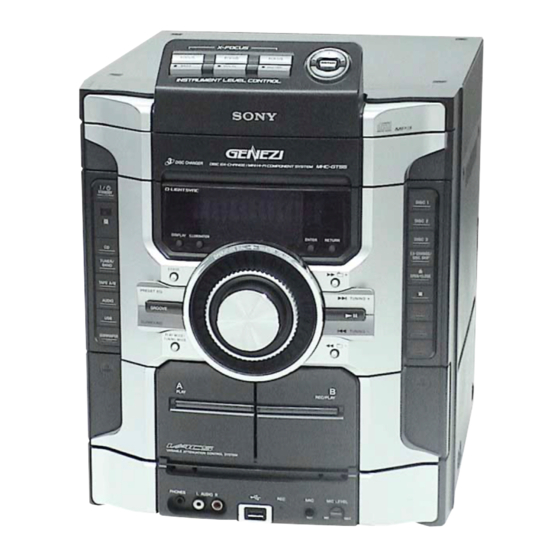
Photo: HCD-GT55
Model Name Using Similar Mechanism
CD
CD Mechanism Type
Section
Base Unit Name
Optical Pick-up Block Name
TAPE
Model Name Using Similar Mechanism
Section
Tape Transport Mechanism Type
Q Q
3
6 7
1 3
SPECIFICATIONS
Power output (rated): 110 W + 110 W
(at 6 Ω, 1 kHz, 1% THD)
RMS output power (reference):
200 W + 200 W (per channel at 6 Ω,
1 kHz, 10% THD)
COMPACT DISC DECK RECEIVER
.
9 4
2 8
HCD-GT22/GT44/GT55
Australian Model
NEW
CDM74KF-K6BD91UR-WOD
BU-K6BD91UR-WOD74
KSM-213DCP
NEW
CWN42FF609
1 5
0 5
8
2 9
9 4
USB section
Supported bit rate
MP3 (MPEG 1 Audio Layer-3):
32 – 320 kbps, VBR
Sampling frequencies
MP3 (MPEG 1 Audio Layer-3):
32/44.1/48 kHz
Transfer speed
Full-Speed
Supported USB device
Mass Storage Class
Maximum current
500 mA
CD player section
System: Compact disc and digital audio
system
Laser: Semiconductor laser (λ=770 –
810 nm)
Emission duration: continuous
Frequency response: 20 Hz – 20 kHz
Signal-to-noise ratio: More than 90 dB
Dynamic range: More than 88 dB
– Continued on next page –
m
co
9 9
E Model
HCD-GT22/GT44
2 8
9 9
Advertisement
Table of Contents

Related Manuals for Sony HCD-GT22


Summary of Contents for Sony HCD-GT22
- Page 1 HCD-GT22/GT44/GT55 Australian Model Ver. 1.0 2007.06 HCD-GT22/GT44 • HCD-GT22 is the amplifier, USB, CD player, tape deck and tuner section in MHC-GT22. • HCD-GT44 is the amplifier, USB, CD player, tape deck and tuner section in MHC-GT44. • HCD-GT55 is the amplifier, USB, CD player, tape deck and tuner section in MHC-GT55.
- Page 2 WITH MARK 0 ON THE SCHEMATIC DIAGRAMS AND IN as a CLASS 1 THE PARTS LIST ARE CRITICAL TO SAFE OPERATION. LASER product. REPLACE THESE COMPONENTS WITH SONY PARTS WHOSE This marking is PART NUMBERS APPEAR AS SHOWN IN THIS MANUAL OR located on the rear IN SUPPLEMENTS PUBLISHED BY SONY.
-
Page 3: Table Of Contents
HCD-GT22/GT44/GT55 3 7 63 1515 0 TABLE OF CONTENTS SERVICING NOTES 7-24. Printed Wiring Boards ..........4 – SUB WOOFER Section (GT44/GT55) – ..... 48 7-25. Schematic Diagram GENERAL ..............6 – SUB WOOFER Section (GT44/GT55) – ..... 49 7-26. -
Page 4: Servicing Notes
HCD-GT22/GT44/GT55 SECTION 1 SERVICING NOTES 3 7 63 1515 0 MODEL IDENTIFICATION NOTES ON HANDLING THE OPTICAL PICK-UP – Model Number Label – BLOCK OR BASE UNIT The laser diode in the optical pick-up block may suffer electrostatic break-down because of the potential difference generated by the charged electrostatic load, etc. - Page 5 HCD-GT22/GT44/GT55 3 7 63 1515 0 SERVICE POSITION In checking the CD mechanism deck, prepare jig (extension cable J-2501-248-A (27 core/300 mm))/J-2501-077-A (13 core/300 mm) MAIN board Connect jig (extension cable J-2501-248-A) to the flexible flat cable (27 core) and CD board (CN202).
-
Page 6: General
HCD-GT22/GT44/GT55 SECTION 2 This section is extracted from instruction manual. GENERAL 3 7 63 1515 0 • Location of Controls Unit Remote HCD-GT55 Unit: PRESET EQ, Press to select the CD function. GROOVE, SURROUND Remote: EQ TUNER/BAND Press to select the sound effect. -
Page 7: Disassembly
HCD-GT22/GT44/GT55 SECTION 3 DISASSEMBLY 3 7 63 1515 0 • This set can be disassembled in the order shown below. 3-1. DISASSEMBLY FLOW 3-2. CASE (SIDE-L), CASE (SIDE-R) (Page 8) 3-3. CASE (TOP) (Page 8) 3-4. LID (CD) (Page 9) 3-5. -
Page 8: Case (Side-L), Case (Side-R)
HCD-GT22/GT44/GT55 3 7 63 1515 0 Note: Follow the disassembly procedure in the numerical order given. 3-2. CASE (SIDE-L), CASE (SIDE-R) 3 case (side-L) 2 two screws (BVTP3 × 10) 1 three screws (case 3 TP2) 6 case (side-R) 5 two screws (BVTP3 ×... -
Page 9: Lid (Cd)
HCD-GT22/GT44/GT55 3 7 63 1515 0 3-4. LID (CD) 3 four claws 4 lid (CD) 1 Turn the gear (loading A) to the direction of the arrow. 3-5. CD MECHANISM DECK (CDM74KF-K6BD91UR-WOD), USB BOARD L 13942296513 8 CD mechanism deck... -
Page 10: Front Panel Block
HCD-GT22/GT44/GT55 3 7 63 1515 0 3-6. FRONT PANEL BLOCK 6 front panel block 4 two connectors (CN301, CN302) 1 flexible flat cable (27 core) (CN901) 2 flexible flat cable (11 core) (CN201) 3 flexible flat cable (13 core) -
Page 11: Back Panel Block
HCD-GT22/GT44/GT55 3 7 63 1515 0 3-8. BACK PANEL BLOCK 5 back panel block 1 flexible flat cable (9 core) 3 connector (tuner (FM/AM)) (CN701) (except Australian model) 2 connector 4 two screws (CN041) (BVTP3 × 10) (GT44/GT55) 4 two screws (BVTP3 ×... -
Page 12: Cd Board
HCD-GT22/GT44/GT55 3 7 63 1515 0 3-10. CD BOARD 1 screw 2 screw (BVTP3 × 8) (BVTP2.6) 6 CD board 3 cover (OP) 4 flexible flat (16 core) cable (CN301) 5 Remove soldering from the four points. CD machanism deck... -
Page 13: Optical Pick-Up Block (Ksm-213D)
HCD-GT22/GT44/GT55 3 7 63 1515 0 3-12. OPTICAL PICK-UP BLOCK (KSM-213D) 1 floating screw (PTPWH M2.6) 5 two insulators 2 h older (213) assy qd optical pick-up block 4 two coil springs (KSM-213D) (insulator) 8 two insulators 7 two coil springs... -
Page 14: Motor (Tb) Board
HCD-GT22/GT44/GT55 3 7 63 1515 0 3-14. MOTOR (TB) BOARD 2 stopper 1 stopper 7 t able motor assy (M741) 3 wire (flat type) (5 core) (CN742) 8 MOTOR (TB) board 6 Remove the two solderings of motor. 5 two screws (BTTP (M2.6)) -
Page 15: Test Mode
HCD-GT22/GT44/GT55 SECTION 4 TEST MODE 3 7 63 1515 0 COLD RESET AMP TEST MODE The cold reset clears all data including preset data stored in the This mode is used to display the parameter of amplifier IC and RAM to initial conditions. - Page 16 Table operation time-out (Table does not move to the target are displayed on the fluorescent indicator tube. position within the specified time) *1) GRL2H : HCD-GT22 In the chucking down operation, the operation was retried GRL2HS : HCD-GT44 by the maximum number of times but the operation could...
- Page 17 HCD-GT22/GT44/GT55 3 7 63 1515 0 5 REPEAT LIMIT CANCEL MODE The 9th and 10 th digit from the left indicates: (Tray status display) Number of repeat for CD playback is 5 times when the repeat mode The 9th and 10th digit from the left indicates which target processing is “REPEAT”.
- Page 18 HCD-GT22/GT44/GT55 3 7 63 1515 0 PANEL TEST MODE This mode is used to check the fluorescent indicator tube, LEDs, phones jack, keys and control knobs. Procedure: 1. Press the button to turn the power on. , [SURROUND] and [TUNER] simultaneously.
-
Page 19: Mechanical Adjustments
HCD-GT22/GT44/GT55 SECTION 5 MECHANICAL ADJUSTMENTS 3 7 63 1515 0 PRECAUTION 1. Clean the following parts with a denatured-alcohol-moistened swab : record/playback head pinch roller erase head rubber belts capstan idlers 2. Demagnetize the record/playback head with a head demagnetizer. -
Page 20: Electrical Adjustments
HCD-GT22/GT44/GT55 SECTION 6 ELECTRICAL ADJUSTMENTS 3 7 63 1515 0 4. After the adjustments, apply suitable locking compound to DECK SECTION 0 dB=0.775 V the pats adjusted. 1. Demagnetize the record/playback head with a head Adjustment Location: Playback Head (DECK-A) demagnetizer. - Page 21 HCD-GT22/GT44/GT55 3 7 63 1515 0 TUNER SECTION CD SECTION FM TUNE LEVEL CHECK Note: 1. CD Block is basically constructed to operate without adjustment. 2. Use YEDS-18 disc (3-702-101-01) unless otherwise indicated. signal generator 3. Use an oscilloscope with more than 10 MΩ impedance.
- Page 22 HCD-GT22/GT44/GT55 3 7 63 1515 0 MEMO L 13942296513 u163 http://www.xiaoyu163.com...
-
Page 23: Block Diagram - Cd Servo, Usb Section
HCD-GT22/GT44/GT55 SECTION 7 3 7 6 3 1 5 1 5 0 DIAGRAMS 7-1. BLOCK DIAGRAM – CD SERVO, USB Section – DETECTOR BD+3.3V FNi1 (A) 97 FPi1 (B) CD-L (Page 24) AGCi RFEQo 81 RFi 94 FNi2 (C) -
Page 24: Block Diagram - Main Section
HCD-GT22/GT44/GT55 3 7 6 3 1 5 1 5 0 7-2. BLOCK DIAGRAM – MAIN Section – AUDIO+9V R-ch is omitted due to same as L-ch. • Abbreviation RV801 SIGNAL PATH AR : Argentina model MIC LEVEL E2 : 120V AC Area in E model... -
Page 25: Block Diagram - Amp Section
HCD-GT22/GT44/GT55 3 7 6 3 1 5 1 5 0 7-3. BLOCK DIAGRAM – AMP Section – HP IN (Page 24) AUDIO+9V J803 R-CH PHONES BASS AGC R-CH (Page 24) IC441 (GT22/GT55) IC441 (GT44) JK441 –1 BUFFER POWER AMP... -
Page 26: Block Diagram - Panel, Power Amp Section
HCD-GT22/GT44/GT55 3 7 6 3 1 5 1 5 0 7-4. BLOCK DIAGRAM – PANEL, POWER AMP Section – PT901 MAIN POWER TRANSFORMER FLUORESCENT INDICATOR D908 TUBE –27V –VFL REGULATOR FLUORESCENT INDICATOR Q902 TUBE DRIVER SYSTEM CONTROLLER IC701 IC901 (4/4) - Page 27 HCD-GT22/GT44/GT55 3 7 6 3 1 5 1 5 0 • Note For Printed Wiring Boards and Schematic Diagrams • Circuit Boards Location Note on Printed Wiring Board: Note on Schematic Diagram: • X : parts extracted from the component side.
-
Page 28: Printed Wiring Board - Cd Board
HCD-GT22/GT44/GT55 3 7 6 3 1 5 1 5 0 • See page 27 for Circuit Boards Location. 7-5. PRINTED WIRING BOARD – CD Board – : Uses unleaded solder. CD BOARD (CONDUCTOR SIDE) CD BOARD (COMPONENT SIDE) M401... -
Page 29: Schematic Diagram - Cd Board
HCD-GT22/GT44/GT55 3 7 6 3 1 5 1 5 0 7-6. SCHEMATIC DIAGRAM – CD Board – • See page 36 for Waveforms. • See page 58 for IC Block Diagrams. • See page 61 for IC Pin Function Description. -
Page 30: Printed Wiring Boards - Changer Section
HCD-GT22/GT44/GT55 3 7 6 3 1 5 1 5 0 • See page 27 for Circuit Boards Location. 7-7. PRINTED WIRING BOARDS – CHANGE Section – : Uses unleaded solder. • Semiconductor Location Ref. No. Location D701 D711 MOTOR (LD) BOARD... -
Page 31: Schematic Diagram - Changer Section
HCD-GT22/GT44/GT55 3 7 6 3 1 5 1 5 0 7-8. SCHEMATIC DIAGRAM – CHANGE Section – • See page 58 for IC Block Diagrams. LOADING MOTOR DRIVE IC701 BA6956AN R702 R701 CN721 CN704 LM-2 LM-2 D701 M751 C751... -
Page 32: Printed Wiring Board - Usb Board
HCD-GT22/GT44/GT55 3 7 6 3 1 5 1 5 0 • See page 27 for Circuit Boards Location. 7-9. PRINTED WIRING BOARD – USB Board – : Uses unleaded solder. USB BOARD (CONDUCTOR SIDE) USB BOARD (COMPONENT SIDE) (NC) -
Page 33: Schematic Diagram - Usb Board
HCD-GT22/GT44/GT55 3 7 6 3 1 5 1 5 0 7-10. SCHEMATIC DIAGRAM – USB Board – • See page 36 for Waveforms. • See page 58 for IC Block Diagrams. • See page 61 for IC Pin Function Description. -
Page 34: Printed Wiring Board - Tc Board
HCD-GT22/GT44/GT55 3 7 6 3 1 5 1 5 0 7-11. PRINTED WIRING BOARD – TC Board – • See page 27 for Circuit Boards Location. : Uses unleaded solder. • Semiconductor Location Ref. No. Location D301 (Page 37) -
Page 35: Schematic Diagram - Tc Board
HCD-GT22/GT44/GT55 3 7 6 3 1 5 1 5 0 • See page 36 for Waveforms 7-12. SCHEMATIC DIAGRAM – TC Board – Q301 2SJ461 TC BOARD PB SWITCH(DECK-A) IC301(1/3) R309 C301 <<4>> NJM14558V-TE2 <<4>> <<4>> 1000p <<4>> {4.2} {4.2}... - Page 36 HCD-GT22/GT44/GT55 3 7 6 3 1 5 1 5 0 • Waveforms – CD Board – – TC Board – – PANEL Board – IC101 ia (RFi) Q453 (Base) (REC mode) IC701 rh (XTb) (CD play mode) 3.2 Vp-p 2.1 Vp-p...
-
Page 37: Printed Wiring Boards - Main Section
HCD-GT22/GT44/GT55 3 7 6 3 1 5 1 5 0 • See page 27 for Circuit Boards Location. 7-13. PRINTED WIRING BOARDS – MAIN Section – : Uses unleaded solder. • Semiconductor Location Ref. No. Location Ref. No. Location... -
Page 38: Schematic Diagram - Main Section (1/4)
HCD-GT22/GT44/GT55 3 7 6 3 1 5 1 5 0 • See page 36 for Waveforms. • See page 61 for IC Pin Function Description. 7-14. SCHEMATIC DIAGRAM – MAIN Section (1/4) – MAIN BOARD (1/4) G-OUT R963 R958... -
Page 39: Schematic Diagram - Main Section (2/4)
HCD-GT22/GT44/GT55 3 7 6 3 1 5 1 5 0 • See page 58 for IC Block Diagrams. 7-15. SCHEMATIC DIAGRAM – MAIN Section (2/4) – MAIN BOARD (2/4) MAIN R124 2.2k BOARD MAIN (3/4) BOARD (1/4) R128 (Page... -
Page 40: Schematic Diagram - Main Section (3/4)
HCD-GT22/GT44/GT55 3 7 6 3 1 5 1 5 0 7-16. SCHEMATIC DIAGRAM – MAIN Section (3/4) – • See page 58 for IC Block Diagrams. MAIN BOARD (3/4) CN301 DATA DO(RST) R330 DI(CTS) USB-SO(TXD) USB-SI(RXD) R332 A-IN R327... -
Page 41: Schematic Diagram - Main Section (4/4)
HCD-GT22/GT44/GT55 3 7 6 3 1 5 1 5 0 7-17. SCHEMATIC DIAGRAM – MAIN Section (4/4) – MAIN BOARD (4/4) ∗ R254 10k(GT22/GT55) C273 (GT44/GT55) R278 R279 ∗ 4.7k(GT44) 0.01 R279 4.7k 18k(GT44) 15k(GT55) C274 ∗ R252 C277... -
Page 42: Printed Wiring Board - Mic Board
HCD-GT22/GT44/GT55 3 7 6 3 1 5 1 5 0 • See page 27 for Circuit Boards Location. 7-18. PRINTED WIRING BOARD – MIC Board – : Uses unleaded solder. (Page 37) (Page 32) USB BOARD MAIN BOARD CN903... -
Page 43: Schematic Diagram - Mic Board
HCD-GT22/GT44/GT55 7-19. SCHEMATIC DIAGRAM – MIC Board – 3 7 6 3 1 5 1 5 0 MIC BOARD R802 C807 C805 C806 R807 4.7k C810 R811 C804 R803 220p IC801 1000p 100k 0.022 0.022 100k Q801 NJM4558V-TE2 R809... -
Page 44: Printed Wiring Board
HCD-GT22/GT44/GT55 3 7 6 3 1 5 1 5 0 • See page 27 for Circuit Boards Location. 7-20. PRINTED WIRING BOARD – AMP Board (GT22/GT55) – : Uses unleaded solder. • Semiconductor Location Ref. No. Location D401 JK441... -
Page 45: Schematic Diagram - Amp Board (Gt22/Gt55)
HCD-GT22/GT44/GT55 3 7 6 3 1 5 1 5 0 • See page 58 for IC Block Diagrams. 7-21. SCHEMATIC DIAGRAM – AMP Board (GT22/GT55) – IC441 STK415-130 AMP BOARD IC441 IC B/D POWER AMP D447 30PRA20FC D446 D448... -
Page 46: Printed Wiring Board - Amp Board (Gt44)
HCD-GT22/GT44/GT55 3 7 6 3 1 5 1 5 0 • See page 27 for Circuit Boards Location. 7-22. PRINTED WIRING BOARD – AMP Board (GT44) – : Uses unleaded solder. JK441 SPEAKER AMP BOARD R407 R417 JW465 JL413... -
Page 47: Schematic Diagram - Amp Board (Gt44)
HCD-GT22/GT44/GT55 3 7 6 3 1 5 1 5 0 • See page 58 for IC Block Diagrams. 7-23. SCHEMATIC DIAGRAM – AMP Board (GT44) – IC B/D IC441 AMP BOARD POWER AMP IC441 STK403-130-E R449 1/2W L441 1.7uH... -
Page 48: Printed Wiring Boards - Sub Woofer Section (Gt44/Gt55)
HCD-GT22/GT44/GT55 3 7 6 3 1 5 1 5 0 • See page 27 for Circuit Boards Location. 7-24. PRINTED WIRING BOARDS – SUB WOOFER Section (GT44/GT55) – : Uses unleaded solder. (GT55) (GT44) (Page 44) (Page 46) SW-SP BOARD... -
Page 49: Schematic Diagram - Sub Woofer Section (Gt44/Gt55)
HCD-GT22/GT44/GT55 3 7 6 3 1 5 1 5 0 • See page 58 for IC Block Diagrams. 7-25. SCHEMATIC DIAGRAM – SUB WOOFER Section (GT44/GT55) – SUB WOOFER BOARD IC501 STK404-130S IC501 IC B/D POWER AMP D507 R531 4.7k... -
Page 50: Printed Wiring Boards - Panel Section
HCD-GT22/GT44/GT55 3 7 6 3 1 5 1 5 0 • See page 27 for Circuit Boards Location. 7-26. PRINTED WIRING BOARDS – PANEL Section – : Uses unleaded solder. PANEL BOARD Q714 R714 JW603 C732 R713 FL701 R715... -
Page 51: Schematic Diagram - Panel Section
HCD-GT22/GT44/GT55 3 7 6 3 1 5 1 5 0 7-27. SCHEMATIC DIAGRAM – PANEL Section – • See page 36 for Waveforms. • See page 58 for IC Block Diagrams. FL701 PANEL BOARD FLUORESCENT INDICATOR TUBE 10 11 12... -
Page 52: Printed Wiring Boards - Key Section
HCD-GT22/GT44/GT55 3 7 6 3 1 5 1 5 0 • See page 27 for Circuit Boards Location. : Uses unleaded solder. 7-28. PRINTED WIRING BOARDS – KEY Section – KEY LEFT BOARD KEY RIGHT BOARD S602 – 608, S628, 631 –... -
Page 53: Schematic Diagram - Key Section
HCD-GT22/GT44/GT55 3 7 6 3 1 5 1 5 0 7-29. SCHEMATIC DIAGRAM – KEY Section – KEY TOP BOARD R644 R645 R647 R641 R642 R643 R646 R648 1.5k 2.2k 4.7k S641 S642 S643 S644 S645 S646 S647 S648... -
Page 54: Printed Wiring Board
HCD-GT22/GT44/GT55 3 7 6 3 1 5 1 5 0 • See page 27 for Circuit Boards Location. 7-30. PRINTED WIRING BOARD – TRANS Board (GT22/GT55) – : Uses unleaded solder. JL914 R915 Q903 R904 Q902 JW923 D906 FH916... -
Page 55: Schematic Diagram
HCD-GT22/GT44/GT55 3 7 6 3 1 5 1 5 0 7-31. SCHEMATIC DIAGRAM – TRANS Board (GT22/GT55) – TRANS BOARD GT22:MX,AR,AUS/ GT55:MX,AR PT901 (GT22:AUS) MAIN POWER JW907 JW902 TRANSFORMER F909 T8AL 250V FH910 JL919 FH909 JW901 GT22:E2,E3,E13,E51/ F905 GT55:E2,E51 T6.3AL 250V... -
Page 56: Printed Wiring Board - Trans Board (Gt44)
HCD-GT22/GT44/GT55 3 7 6 3 1 5 1 5 0 • See page 27 for Circuit Boards Location. : Uses unleaded solder. 7-32. PRINTED WIRING BOARD – TRANS Board (GT44) – TRANS BOARD RY901 CN901 R910 R911 R908 JL914... -
Page 57: Schematic Diagram - Trans Board (Gt44)
HCD-GT22/GT44/GT55 3 7 6 3 1 5 1 5 0 7-33. SCHEMATIC DIAGRAM – TRANS Board (GT44) – TRANS BOARD (AUS) (MX,AR,AUS) JW907 JW902 (AR) JW908 (E2,E3,E13,E51) (E2,E3,E13,E51) JW912 JW901 PT901 (E2,E3,E13,E51,MX) MAIN POWER JW909 TRANSFORMER (E2,E3,E13,E51) F909 CN903... - Page 58 HCD-GT22/GT44/GT55 3 7 6 3 1 5 1 5 0 • IC Block Diagrams – MAIN Board – – CD Board – IC401 BA5826SFP-E2 IC201 TK63115SCL-G@GL IC102 R2S15208SP VO1(–) REFIN 1 REF AMP REFOUT VIN 1 D.BUFF VO4(–) THERMAL &...
- Page 59 HCD-GT22/GT44/GT55 3 7 63 1515 0 IC301, 302 TC74HC4066AFT (EL) IC303 TC74VHC157FT (EKJ) SELECT 11 1 1I/O 1A 2 STROBE INPUT 1O/I 2 INPUT OUTPUT 2O/I 3 4I/O 11 12 OUTPUT INPUT 2I/O 4 4O/I INPUT OUTPUT 2C 5...
- Page 60 HCD-GT22/GT44/GT55 3 7 63 1515 0 – PANEL Board – IC701 NJU3427FA2 51 50 49 48 46 45 RESET SERIAL CIRCUIT BUFFER INSTRUCTION TIMING DUTY DECODER COUNTER COUNTER ADDRESS DISPLAY DR35 COUNTER DATA RAM DR34 DR33 DR32 SEGMENT TIMING...
- Page 61 HCD-GT22/GT44/GT55 3 7 63 1515 0 • IC Pin Function Description CD BOARD IC101 TC94A70FG-008 (S, D) (CD-MP3 PROCESSOR) Pin No. Pin Name Description AVSS3 Ground terminal RFZi RF ripple zero crossing signal input terminal RFRP RF ripple signal output terminal...
- Page 62 HCD-GT22/GT44/GT55 3 7 63 1515 0 Pin No. Pin Name Description PIO0 Request signal output to the system controller or USB controller 49, 50 PIO1, PIO2 Not used PIO3 Gate signal input from the USB controller VSS1 Ground terminal VDDT3 Power supply terminal (+3.3 V)
- Page 63 HCD-GT22/GT44/GT55 3 7 63 1515 0 Pin No. Pin Name Description FNi1 (A) Main beam (A) input from the optical pick-up block FPi2 (D) Main beam (D) input from the optical pick-up block FPi1 (B) Main beam (B) input from the optical pick-up block...
- Page 64 HCD-GT22/GT44/GT55 3 7 63 1515 0 USB BOARD IC901 TMP92CD28AFG-2CB4 (USB CONTROLLER) Pin No. Pin Name Description /RESET Reset signal input from the system controller "L": reset Ready to send signal input from the system controller 3, 4 NO USE Not used Function selection signal input terminal Fixed at "H"...
- Page 65 HCD-GT22/GT44/GT55 3 7 63 1515 0 Pin No. Pin Name Description NO USE Not used DVSS Ground terminal Clear to send signal output to the system controller DATA Audio data input from the CD-MP3 processor CLOCK Audio data transfer clock signal input from CD-MP3 processor...
- Page 66 HCD-GT22/GT44/GT55 3 7 63 1515 0 MAIN BOARD IC901 uPD78F1165GF (S)-GAS-AX (SYSTEM CONTROLLER) Pin No. Pin Name Description O-SYS-MUTE Muting on/off control signal output terminal "L": muting on O-SWR Sub woofer speaker on/off relay drive signal output terminal (GT44/GT55)
- Page 67 HCD-GT22/GT44/GT55 3 7 63 1515 0 Pin No. Pin Name Description Serial data transfer clock signal output to the electrical volume and parametric equalizer (GT55) O-AUDIO-CLK Serial data transfer clock signal output to the electrical volume (GT22/GT44) Deck-A/B selection and recording/playback selection signal output terminal O-REC/PB "L": deck-B and playback, "H": deck-A and recording...
- Page 68 HCD-GT22/GT44/GT55 3 7 63 1515 0 Pin No. Pin Name Description Sub system clock output terminal (32.768 kHz) Sub system clock input terminal (32.768 kHz) FLMD0 Not used Main system clock output terminal (20 MHz) Main system clock input terminal (20 MHz)
-
Page 69: Exploded Views
HCD-GT22/GT44/GT55 SECTION 8 EXPLODED VIEWS 3 7 63 1515 0 NOTE: • -XX and -X mean standardized parts, so they • Items marked “*” are not stocked since they : 120V AC area in E model may have some difference from the original are seldom required for routine service. -
Page 70: Key Top Board Section
Description Remark Ref. No. Part No. Description Remark 3-087-053-01 +BVTP2.6 (3CR) 4-217-485-21 EMBLEM (5-A), SONY 2-892-160-01 PANEL (HEAD-B) (GT22/GT44) u163 X-2179-679-1 BUTTON FOCUS ASSY 2-892-159-01 PANEL (HEAD-A) (GT55) (BASS, VOCAL, GUITAR, ENTER, –) (GT55) 2-892-297-01 BUTTON (FOCUS) TOP (FOCUS, FOCUS, FOCUS, +) (GT55) -
Page 71: Tc Mecha Deck Section
HCD-GT22/GT44/GT55 3 7 63 1515 0 8-3. TC MECHA DECK SECTION not supplied not supplied supplied not supplied not supplied L 13942296513 PANEL board section Ref. No. Part No. Description Remark Ref. No. Part No. Description Remark u163 1-417-656-22 MECHA DECK (CWN42FF609) -
Page 72: Panel Board Section
HCD-GT22/GT44/GT55 3 7 63 1515 0 8-4. PANEL BOARD SECTION not supplied (KEY LEFT borad) not supplied (VOLUME board) not supplied (KEY RIGHT board) S651 supplied with S651 not supplied L 13942296513 not supplied (MIC board) front panel section Ref. -
Page 73: Front Panel Section
HCD-GT22/GT44/GT55 3 7 63 1515 0 8-5. FRONT PANEL SECTION not supplied L 13942296513 not supplied Note 1: Ref. No. 203 and Ref. No. 233 are parts glued together. When you exchange Ref. No. 203 or Ref. No. 233, exchange simultaneously. -
Page 74: Main Board Section
HCD-GT22/GT44/GT55 3 7 63 1515 0 8-6. MAIN BOARD SECTION not supplied (GT22: E2, E3, E13, E51, MX, AR/ GT44: E2, E3, E13, E51, MX, AR/ GT55) not supplied (D-LIGHT SYNC board) (GT44/GT55) not supplied M001 POWER board, SUB WOOFER board section... -
Page 75: Power Board, Sub Woofer Board Section
HCD-GT22/GT44/GT55 3 7 63 1515 0 8-7. POWER BOARD, SUB WOOFER BOARD SECTION (GT44/GT55) not supplied not supplied (SUB WOOFER board) not supplied not supplied not supplied (5V REG board) not supplied L 13942296513 (AMP board) not supplied not supplied u163 Ref. -
Page 76: Chassis Section
HCD-GT22/GT44/GT55 3 7 63 1515 0 8-8. CHASSIS SECTION (GT22/GT55) F908 F904 F905 PT901 (GT22/GT55) not supplied (TRANS board) F907 F909 F906 not supplied L 13942296513 not supplied not supplied (TC board) Ref. No. Part No. Description Remark Ref. No. -
Page 77: Cd Mechanism Deck Section-1 (Cdm74Kf-K6Bd91Ur-Wod)
HCD-GT22/GT44/GT55 3 7 63 1515 0 8-9. CD MECHANISM DECK SECTION-1 (CDM74KF-K6BD91UR-WOD) L 13942296513 M741 optical pick-up section Ref. No. Part No. Description Remark Ref. No. Part No. Description Remark 4-218-253-62 SCREW (M2.6), +BTTP 4-243-819-01 GEAR (GENEVA) 1-828-938-51 WIRE (FLAT TYPE) (5 CORE) -
Page 78: Cd Mechanism Deck Section-2 (Cdm74Kf-K6Bd91Ur-Wod)
HCD-GT22/GT44/GT55 3 7 63 1515 0 8-10. CD MECHANISM DECK SECTION-2 (CDM74KF-K6BD91UR-WOD) S711 not supplied M751 L 13942296513 S201 Ref. No. Part No. Description Remark Ref. No. Part No. Description Remark A-1103-756-B DRIVER BOARD, COMPLETE 4-243-822-02 LEVER (LIFTER) 4-218-253-52 SCREW (M2.6), +BTTP... - Page 79 HCD-GT22/GT44/GT55 SECTION 9 5V REG 3 7 63 1515 0 ELECTRICAL PARTS LIST NOTE: • Due to standardization, replacements in the • RESISTORS : 220V – 230V AC area in E model : Chilean and Peruvian models parts list may be different from the parts All resistors are in ohms.
- Page 80 HCD-GT22/GT44/GT55 3 7 63 1515 0 Ref. No. Part No. Description Remark Ref. No. Part No. Description Remark D402 6-500-360-01 DIODE D10XB20 (GT22/GT55) R411 1-216-797-11 METAL CHIP 1/10W D441 6-500-334-01 DIODE MC2836-T112-1 (GT22/GT55) D443 8-719-404-50 DIODE MA111-TX D445 6-501-179-01 DIODE UDZW-TE17-16B (GT22/GT55)
- Page 81 HCD-GT22/GT44/GT55 3 7 63 1515 0 Ref. No. Part No. Description Remark Ref. No. Part No. Description Remark R467 1-216-797-11 METAL CHIP 1/10W C108 1-164-360-11 CERAMIC CHIP 0.1uF (GT44) C109 1-164-360-11 CERAMIC CHIP 0.1uF 0 R468 1-215-871-11 METAL OXIDE 2.2K...
- Page 82 HCD-GT22/GT44/GT55 D-LIGHT SYNC 3 7 63 1515 0 Ref. No. Part No. Description Remark Ref. No. Part No. Description Remark < CONNECTOR > R208 1-216-809-11 METAL CHIP 1/10W CN202 1-784-835-51 CONNECTOR, FFC (LIF (NON-ZIF)) 27P R209 1-216-809-11 METAL CHIP...
- Page 83 HCD-GT22/GT44/GT55 D-LIGHT SYNC DRIVER KEY LEFT KEY RIGHT 3 7 63 1515 0 Ref. No. Part No. Description Remark Ref. No. Part No. Description Remark < RESISTOR > R751 1-249-425-11 CARBON 4.7K 1/4W ************************************************************ R701 1-216-849-11 METAL CHIP 220K...
- Page 84 HCD-GT22/GT44/GT55 KEY RIGHT KEY TOP MAIN 3 7 63 1515 0 Ref. No. Part No. Description Remark Ref. No. Part No. Description Remark R637 1-216-829-11 METAL CHIP 4.7K 1/10W A-1271-844-A MAIN BOARD, COMPLETE (GT44: E51, AR) A-1271-845-A MAIN BOARD, COMPLETE (GT44: E3, E13) <...
- Page 85 HCD-GT22/GT44/GT55 MAIN 3 7 63 1515 0 Ref. No. Part No. Description Remark Ref. No. Part No. Description Remark C144 1-137-374-11 MYLAR 0.047uF C182 1-126-947-11 ELECT 47uF (GT44/GT55) C145 1-162-968-11 CERAMIC CHIP 0.0047uF 10% C211 1-126-961-11 ELECT 2.2uF C146 1-162-968-11 CERAMIC CHIP 0.0047uF 10%...
- Page 86 HCD-GT22/GT44/GT55 MAIN 3 7 63 1515 0 Ref. No. Part No. Description Remark Ref. No. Part No. Description Remark < CONNECTOR > IC303 6-707-870-01 IC TC74VHC157FT (EKJ) CN002 1-815-444-11 PIN, CONNECTOR (PWB) 3P IC901 (Not supplied) IC uPD78F1165GF (S)-GAS-AX...
- Page 87 HCD-GT22/GT44/GT55 MAIN 3 7 63 1515 0 Ref. No. Part No. Description Remark Ref. No. Part No. Description Remark Q921 8-729-620-07 TRANSISTOR 2SC3052EF-T1-LEF (GT55) R129 1-216-842-11 METAL CHIP 1/10W Q922 8-729-620-07 TRANSISTOR 2SC3052EF-T1-LEF (GT55) (GT22: E3, E13, E51, MX, AR, AUS/GT44: E3, E13,...
- Page 88 HCD-GT22/GT44/GT55 MAIN 3 7 63 1515 0 Ref. No. Part No. Description Remark Ref. No. Part No. Description Remark R202 1-216-825-11 METAL CHIP 2.2K 1/10W R279 1-216-836-11 METAL CHIP 1/10W R211 1-216-832-11 METAL CHIP 8.2K 1/10W (GT44) R212 1-216-825-11 METAL CHIP 2.2K...
- Page 89 HCD-GT22/GT44/GT55 MAIN 3 7 63 1515 0 Ref. No. Part No. Description Remark Ref. No. Part No. Description Remark R913 1-216-821-11 METAL CHIP 1/10W R914 1-216-833-11 METAL CHIP 1/10W R974 1-216-809-11 METAL CHIP 1/10W R975 1-216-809-11 METAL CHIP 1/10W...
- Page 90 HCD-GT22/GT44/GT55 MOTOR (LD) MOTOR (TB) PANEL 3 7 63 1515 0 Ref. No. Part No. Description Remark Ref. No. Part No. Description Remark C817 1-164-156-11 CERAMIC CHIP 0.1uF R844 1-216-841-11 METAL CHIP 1/10W C821 1-164-156-11 CERAMIC CHIP 0.1uF R845...
- Page 91 HCD-GT22/GT44/GT55 PANEL 3 7 63 1515 0 Ref. No. Part No. Description Remark Ref. No. Part No. Description Remark D604 6-501-691-01 LED 1L434FV22D0TDF01 (STREAM) R666 1-216-821-11 METAL CHIP 1/10W (GT22/GT44) R671 1-216-821-11 METAL CHIP 1/10W D605 6-501-451-01 LED 1L4344B22COCDT02 (STREAM) (GT55)
- Page 92 HCD-GT22/GT44/GT55 PANEL SENSOR SUB WOOFER 3 7 63 1515 0 Ref. No. Part No. Description Remark Ref. No. Part No. Description Remark < IC > < SWITCH > IC501 6-600-091-01 IC STK404-130S S601 1-762-875-21 SWITCH, KEYBOARD (DISPLAY) S611 1-762-875-21 SWITCH, KEYBOARD (ILLUMINATION) <...
- Page 93 HCD-GT22/GT44/GT55 SW-SP 3 7 63 1515 0 Ref. No. Part No. Description Remark Ref. No. Part No. Description Remark 1-687-669-12 SW BOARD C456 1-130-483-00 MYLAR 0.01uF ********* C461 1-164-315-11 CERAMIC CHIP 470PF C462 1-164-315-11 CERAMIC CHIP 470PF S751 1-786-514-11 SWITCH, LEVER (SLIDE)
- Page 94 HCD-GT22/GT44/GT55 TRANS 3 7 63 1515 0 Ref. No. Part No. Description Remark Ref. No. Part No. Description Remark R440 1-216-833-11 METAL CHIP 1/10W < RESISTOR > R441 1-216-864-11 SHORT CHIP R442 1-216-841-11 METAL CHIP 1/10W R301 1-216-841-11 METAL CHIP...
- Page 95 HCD-GT22/GT44/GT55 TRANS 3 7 63 1515 0 Ref. No. Part No. Description Remark Ref. No. Part No. Description Remark < FUSE HOLDER > C910 1-162-919-11 CERAMIC CHIP 22PF FH907 1-533-217-41 HOLDER, FUSE C912 1-162-915-11 CERAMIC CHIP 10PF 0.5PF FH908...
- Page 96 HCD-GT22/GT44/GT55 VOLUME 3 7 63 1515 0 Ref. No. Part No. Description Remark Ref. No. Part No. Description Remark R932 1-216-809-11 METAL CHIP 1/10W < ROTARY ENCODER > R933 1-216-864-11 SHORT CHIP R934 1-216-833-11 METAL CHIP 1/10W S651 1-480-109-11 ENCODER, ROTARY (MASTER VOLUME)
- Page 97 HCD-GT22/GT44/GT55 3 7 63 1515 0 MEMO L 13942296513 u163 http://www.xiaoyu163.com...
- Page 98 HCD-GT22/GT44/GT55 3 7 63 1515 0 REVISION HISTORY Clicking the version allows you to jump to the revised page. Also, clicking the version at the upper right on the revised page allows you to jump to the next revised page.
Need help?
Do you have a question about the HCD-GT22 and is the answer not in the manual?
Questions and answers