Table of Contents
Advertisement
Quick Links
QQ
3 7 63 1515 0
SERVICE MANUAL
Ver. 1.1 2008.09
• HCD-GTX999 is the amplifi er, USB, CD player,
HDD Jukebox and tuner section in DSK-GTX999.
• "WALKMAN" and "WALKMAN"
logo are registered trademarks of Sony
Corporation.
• MICROVAULT is a trademark of Sony
Corporation.
• MPEG Layer-3 audio coding
technology and patents licensed from
• Title Updater is a trademark of Sony
Corporation.
•
and Windows Media are trademarks
TE
L 13942296513
Corporation in the United States and/
or other countries.
•
intellectual property rights of
distribution of such technology
outside of this product is prohibited
• Built with Linter Database.
Copyright © 2006-2007, Brycen Corp.,
Ltd.
Copyright © 1990-2003, Relex, Inc., All
rights reserved.
• Music recognition technology and
®
related data are provided by Gracenote
Gracenote is the industry standard in music
recognition technology and related content
delivery. For more information, please visit
www.gracenote.com.
CD and music-related data from Gracenote,
Inc., copyright © 2000-2008 Gracenote.
practice one or more of the following U.S.
Patents: #5,987,525; #6,061,680; #6,154,773,
#6,161,132, #6,230,192, #6,230,207,
#6,240,459, #6,330,593, and other patents
issued or pending. Some services supplied
under license from Open Globe, Inc. for U.S.
Patent: #6,304,523.
Gracenote and CDDB are registered
logo and logotype, and the "Powered
by Gracenote" logo are trademarks of
Gracenote.
Gracenote
End User License
®
Agreement
from Gracenote, Inc. of Emeryville, California
information, including name, artist, track,
and title information ("Gracenote Data")
from online servers or embedded databases
(collectively, "Gracenote Servers") and
to perform other functions. You may use
Gracenote Data only by means of the intended
End-User functions of this application or
device.
www
.
Sony Corporation
9-889-164-02
2008I05-1
Audio&Video Business Group
©
2008.09
Published by Sony Techno Create Corporation
http://www.xiaoyu163.com
You agree that you will use Gracenote Data,
for your own personal non-commercial
use only. You agree not to assign, copy,
or any Gracenote Data to any third party.
YOU AGREE NOT TO USE OR EXPLOIT
GRACENOTE DATA, THE GRACENOTE
SOFTWARE, OR GRACENOTE SERVERS,
EXCEPT AS EXPRESSLY PERMITTED
HEREIN.
You agree that your non-exclusive license
to use the Gracenote Data, the Gracenote
if you violate these restrictions. If your license
terminates, you agree to cease any and all use
and Gracenote Servers. Gracenote reserves
all rights in Gracenote Data, the Gracenote
all ownership rights. Under no circumstances
will Gracenote become liable for any payment
to you for any information that you provide.
You agree that Gracenote, Inc. may enforce
its rights under this Agreement against you
directly in its own name.
purpose of a randomly assigned numeric
count queries without knowing anything about
who you are. For more information, see the
.
web page for the Gracenote Privacy Policy for
the Gracenote service.
Gracenote Data are licensed to you "AS IS. "
Gracenote makes no representations or
warranties, express or implied, regarding the
accuracy of any Gracenote Data from in the
Gracenote Servers. Gracenote reserves the right
to delete data from the Gracenote Servers or
to change data categories for any cause that
Servers are error-free or that functioning of
be uninterrupted. Gracenote is not obligated to
provide you with new enhanced or additional
data types or categories that Gracenote may
provide in the future and is free to discontinue
its services at any time.
GRACENOTE DISCLAIMS ALL
WARRANTIES EXPRESS OR IMPLIED,
INCLUDING, BUT NOT LIMITED
TO, IMPLIED WARRANTIES OF
MERCHANTABILITY, FITNESS FOR A
PARTICULAR PURPOSE, TITLE, AND
NON-INFRINGEMENT. GRACENOTE
DOES NOT WARRANT THE RESULTS
THAT WILL BE OBTAINED BY YOUR
USE OF THE GRACENOTE SOFTWARE
OR ANY GRACENOTE SERVER. IN NO
CASE WILL GRACENOTE BE LIABLE FOR
ANY CONSEQUENTIAL OR INCIDENTAL
DAMAGES OR FOR ANY LOST PROFITS OR
LOST REVENUES.
indicated in this manual are generally the
trademarks or registered trademarks of the
manufacturer.
™
®
and
marks are omitted in this manual.
x
ao
y
i
http://www.xiaoyu163.com
HCD-GTX999
8
Model Name Using Similar Drive
CD Mechanism Type
CD Section
Base Unit Name
Optical Pick-up Block Name
Model Name Using Similar Drive
HD Section
Hard Disc Drive Name
Q Q
3
6 7
1 3
Outputs
PHONES (stereo mini jack):
240 V, 50/60 Hz (Latin American models
(except for Brazilian model))
FRONT SPEAKER:
V, 60 Hz
(Mexican model)
V,
SUBWOOFER:
50/60 Hz (Brazilian model)
Except for Brazilian model
Front speaker:
HDD Jukebox section
Power output (rated):
120 W + 120 W (at 6 ohms, 1 kHz,
Capacity:
1% THD)
RMS output power (reference):
200 W + 200 W (per channel at 6
ohms, 1 kHz, 10% THD)
Subwoofer:
Recording system:
RMS output power (reference):
190 W (100 Hz, 10% THD)
Maximum recording time (measured with
MP3 128 kbps):
Brazilian model
Front speaker:
Maximum number of tracks:
Power output (rated):
120 W + 120 W (at 6 ohms, 1 kHz,
Maximum number of albums:
1% THD)
RMS output power (reference):
Supported bit rate:
150 W + 150 W (at 6 ohms, 1 kHz,
10% THD)
Subwoofer:
RMS output power (reference):
190 W (100 Hz, 10% THD)
Sampling frequencies:
Inputs
AUDIO IN L/R (phono jacks):
voltage 250 mV, impedance
47 kilohms
VIDEO AUDIO IN L/R (phono jacks):
voltage 250 mV, impedance
47 kilohms
MIC (phone jack):
sensitivity 1 mV, impedance
10 kilohms
u163
.
2 9
9 4
2 8
NEW
CDM77B-F2BD82F-WAO
BU-F2BD82F-A
KSM215DHAP
NEW
HDD/SG-NIGHTHAWK-S (80GB)
1 5
0 5
8
2 9
9 4
SPECIFICATIONS
USB section
(USB) port:
accepts headphones with an
Type A
impedance of 8 ohms or more
Supported bit rate:
MP3 (MPEG 1 Audio Layer-3):
32 − 320 kbps, VBR
Use only the supplied speaker
WMA: 48 − 192 kbps, VBR
SS-GTX999
AAC: 48 − 320 kbps
Use only the supplied subwoofer
Sampling frequencies:
SS-WG999
MP3 (MPEG 1 Audio Layer-3):
32/44.1/48 kHz
WMA: 44.1 kHz
AAC: 44.1 kHz
80 GB*
CD player section
*A portion of the memory is used for
system management functions. Actual
System:
available memory is approx. 72 GB.
Compact disc and digital audio
system
MP3
Laser Diode Properties
Emission duration: Continuous
Laser Output*: Less than 44.6μW
About 1,300 h
*
20,000
Frequency response:
2,000
20 Hz − 20 kHz
Signal-to-noise ratio:
MP3 (MPEG 1 Audio Layer-3):
32 − 320 kbps, VBR
More than 90 dB
WMA: 48 − 192 kbps, VBR
Dynamic range:
AAC: 48 − 320 kbps
More than 88 dB
MP3 (MPEG 1 Audio Layer-3):
32/44.1/48 kHz
WMA: 44.1 kHz
AAC: 44.1 kHz
– Continued on next page –
m
HDD AUDIO SYSTEM
co
9 9
E Model
2 8
9 9
at a distance of 200mm from the
objective lens surface on the Optical
Pick-up Block with 7mm aperture.
Advertisement
Table of Contents

Related Manuals for Sony HCD-GTX999


Summary of Contents for Sony HCD-GTX999
-
Page 1: Specifications
3 7 63 1515 0 SERVICE MANUAL E Model Ver. 1.1 2008.09 • HCD-GTX999 is the amplifi er, USB, CD player, HDD Jukebox and tuner section in DSK-GTX999. • “WALKMAN” and “WALKMAN” You agree that you will use Gracenote Data,... -
Page 2: Table Of Contents
THE PARTS LIST ARE CRITICAL TO SAFE OPERATION. REPLACE THESE COMPONENTS WITH SONY PARTS ELECTRICAL PARTS LIST ......70 WHOSE PART NUMBERS APPEAR AS SHOWN IN THIS MANUAL OR IN SUPPLEMENTS PUBLISHED BY SONY. Accessories are given in the last of the electrical parts list. http://www.xiaoyu163.com... - Page 3 HCD-GTX999 Ver. 1.1 SECTION 1 SERVICING NOTES 3 7 63 1515 0 NOTE THE IC5 AND IC13 ON THE USB MICOM NOTES ON HANDLING THE OPTICAL PICK-UP BOARD REPLACING BLOCK OR BASE UNIT IC5 and IC13 on the USB MICOM board cannot exchange with single.
- Page 4 HCD-GTX999 3 7 63 1515 0 REPLACEMENT PROCEDURE OF HDD 1. Prior Notes • It is backup in the customer in preparation for the HDD exchange as for the tune recorded to HDD beforehand. • Note that all recorded tunes are deleted when “Factory Reset" is done.
- Page 5 • Rental or used discs with attached seals where the glue extends beyond this may cause the system to malfunction. the seal Sony cannot provide compensation for any loss of data caused by a dam- • Discs that have labels printed using ink that feels tacky when touched aged hard disk drive.
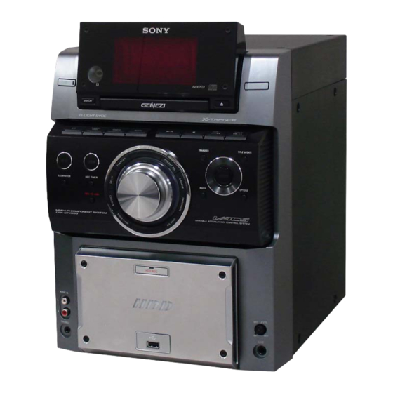
- Page 6 HCD-GTX999 SECTION 2 This section is extracted GENERAL from instruction manual. 3 7 63 1515 0 Guide to parts and controls TRANSFER Unit: HDD REC Remote: HDD REC (start Press to transfer tracks on the HDD recording) Jukebox to an USB device.
- Page 7 HCD-GTX999 3 7 63 1515 0 Display Setting the clock Use buttons on the remote to set the clock. Press / to turn on the system. Press CLOCK/TIMER SET repeatedly to select “CLOCK SET, ” and then press ENTER...
-
Page 8: Disassembly
HCD-GTX999 SECTION 3 DISASSEMBLY 3 7 63 1515 0 • This set can be disassembled in the order shown below. 3-1. DISASSEMBLY FLOW 3-2. CASE (TOP) (Page 8) 3-3. FRONT PANEL BLOCK 3-5. USB MICOM BOARD (Page 9) (Page 10) 3-6. -
Page 9: Front Panel Block
HCD-GTX999 3 7 63 1515 0 3-3. FRONT PANEL BLOCK connector (CN6) connector (CN862) connector (CN861) screw (BVTP3 × 8) connector (CN871) front panel block flexible flat cable (17 core) (CN201) screw (BVTP3 × 8) three screws (BVTP3 × 8) -
Page 10: Usb Micom Board
HCD-GTX999 3 7 63 1515 0 3-5. USB MICOM BOARD four screws plate shield (BVTP3 × 8) (USB MICOM PWB) connector (CN8) four screws harness (BVTP3 × 8) connector USB MICOM board chassis (USB MICOM PWB) flexible flat cable (17 core) -
Page 11: Cd Mechanism Block
HCD-GTX999 3 7 63 1515 0 3-7. CD MECHANISM BLOCK three screws (BVTP3 × 8) two claws CD mechanism block loading panel flexible flat cable (19 core) (CN101) flexible flat cable (5 core) (CN001) L 13942296513 3-8. BRACKET (CDM) BLOCK... -
Page 12: Back Panel Block
HCD-GTX999 Ver. 1.1 3 7 63 1515 0 3-9. BACK PANEL BLOCK back panel block power cord connector (CN401) five screws connector (BVTP3 × 8) (CN402: E2, E51, BR) (CN404: MX, AR) flexible flat cable (9 core) connector (CN403) screw (BVTP3 ×... -
Page 13: Test Mode
HCD-GTX999 SECTION 4 TEST MODE 3 7 63 1515 0 TUNER STEP CHANGE Note: Never execute the item because the set might not operate The AM tuning interval can be changed over 9 kHz or 10 kHz. normally when the item being written, “Not used for the servicing.”... - Page 14 • ROOT\MUSIC\(File of description to “MUJIC\music.txt”) • ROOT\SYSTEM\CCUDB\SCCU.IDX • ROOT\SYSTEM\CCUDB\SCCUTOC.IDX 6. Initialization Mode For Factory The user use areas other than the “Sony Demo” artist in HDD are initialized, and the cold reset is executed. Procedure: 1. Enter the HDD test mode.
-
Page 15: Electrical Checks
HCD-GTX999 SECTION 5 ELECTRICAL CHECKS 3 7 6 3 1 5 1 5 0 HDD FACTORY SHIPMENT TEST MODE Connecting and Adjustment Location: CD board CD SECTION The user use areas in HDD are initialized, and the cold reset is –... -
Page 16: Diagrams
HCD-GTX999 SECTION 6 DIAGRAMS 3 7 6 3 1 5 1 5 0 6-1. BLOCK DIAGRAM - CD SERVO, PANEL Section - DISPLAY CONTROLLER IC701 DIGITAL SERVO, DIGITAL SIGNAL PROCESSOR, D/A CONVERTER OPTICAL PICK-UP IC201 D607, 608 BLOCK LED DRIVE... -
Page 17: Block Diagram - Usb, Hdd Section
HCD-GTX999 3 7 6 3 1 5 1 5 0 6-2. BLOCK DIAGRAM - USB, HDD Section - DATA BUFFER IC11 USB SYSTEM CONTROLLER IC2 (2/2) A/D CONVERTER, D/A CONVERTER IC12 (Page 18) VOUTL LRCKO 12 LRCKI SDTI 8 DOUT VOUTR R–CH... -
Page 18: Block Diagram - Main Section
HCD-GTX999 3 7 6 3 1 5 1 5 0 6-3. BLOCK DIAGRAM - MAIN Section - RV871 R-ch is omitted due to same as L-ch. MIC LEVEL SIGNAL PATH J871 MIC AMP MIC AMP : TUNER (FM/AM) IC871 (1/2) -
Page 19: Block Diagram - Amp Section
HCD-GTX999 3 7 6 3 1 5 1 5 0 6-4. BLOCK DIAGRAM - AMP Section - J861 R-CH PHONES BASS AGC (Page 18) R-CH TB501 –1 (Page 18) – FRONT SPEAKER ONLY FOR – SS-GTX999 –2 MUTING TH501... -
Page 20: Block Diagram - Power Supply Section
HCD-GTX999 Ver. 1.1 3 7 6 3 1 5 1 5 0 6-5. BLOCK DIAGRAM - POWER SUPPLY Section - T420 MAIN POWER TRANSFORMER FLUORESCENT INDICATOR D421 TUBE REGULATOR +VFL Q421 F421 RECT F427 –VH D501 SYSTEM CONTROLLER SECTION... - Page 21 HCD-GTX999 Ver. 1.1 3 7 6 3 1 5 1 5 0 THIS NOTE IS COMMON FOR PRINTED WIRING BOARDS AND SCHEMATIC DIAGRAMS. • Circuit Boards Location (In addition to this, the necessary note is printed in each block.) For Printed Wiring Boards.
-
Page 22: Printed Wiring Board - Cd Board
HCD-GTX999 3 7 6 3 1 5 1 5 0 6-6. PRINTED WIRING BOARD - CD Board - • See page 21 for Circuit Boards Location. • : Uses unleaded solder. (Page 30) IC201 1 3 9 4 2 2 9 6 5 1 3... -
Page 23: Schematic Diagram - Cd Board
HCD-GTX999 3 7 6 3 1 5 1 5 0 6-7. SCHEMATIC DIAGRAM - CD Board - • See page 35 for waveforms. • See page 48 for IC Block Diagrams. CD BOARD R302 CN301 TP313 R301 C301 TP312... -
Page 24: Printed Wiring Board - Usb Micom Board
HCD-GTX999 6-8. PRINTED WIRING BOARD - USB MICOM Board - • See page 21 for Circuit Boards Location. • : Uses unleaded solder. 3 7 6 3 1 5 1 5 0 USB MICOM BOARD (SIDE A) USB MICOM BOARD... -
Page 25: Schematic Diagram - Usb Micom Board (1/4)
HCD-GTX999 6-9. SCHEMATIC DIAGRAM - USB MICOM Board (1/4) - • See page 35 for waveforms. • See page 48 for IC Block Diagrams. • See page 55 for IC Pin Function Description. 3 7 6 3 1 5 1 5 0... -
Page 26: Schematic Diagram - Usb Micom Board (2/4)
HCD-GTX999 6-10. SCHEMATIC DIAGRAM - USB MICOM Board (2/4) - • See page 48 for IC Block Diagrams. • See page 55 for IC Pin Function Description. 3 7 6 3 1 5 1 5 0 USB MICOM BOARD... -
Page 27: Schematic Diagram - Usb Micom Board (3/4)
HCD-GTX999 6-11. SCHEMATIC DIAGRAM - USB MICOM Board (3/4) - • See page 35 for waveforms. • See page 48 for IC Block Diagrams. 3 7 6 3 1 5 1 5 0 (Page 25) (Page 26) USB MICOM... -
Page 28: Q Q 6-12. Schematic Diagram - Usb Micom Board (4/4)
HCD-GTX999 6-12. SCHEMATIC DIAGRAM - USB MICOM Board (4/4) - • See page 35 for waveforms. • See page 48 for IC Block Diagrams. • See page 55 for IC Pin Function Description. 3 7 6 3 1 5 1 5 0... -
Page 29: Printed Wiring Boards - Usb, Led Section
HCD-GTX999 6-13. PRINTED WIRING BOARDS - USB, LED Section - 6-14. SCHEMATIC DIAGRAM - USB, LED Section - 3 7 6 3 1 5 1 5 0 • See page 21 for Circuit Boards Location. • : Uses unleaded solder. -
Page 30: Printed Wiring Board - Main Board
HCD-GTX999 Ver. 1.1 6-15. PRINTED WIRING BOARD - MAIN Board - • See page 21 for Circuit Boards Location. • : Uses unleaded solder. 3 7 6 3 1 5 1 5 0 • Semiconductor (Page 35) (Page 24) -
Page 31: Schematic Diagram - Main Board (1/3)
HCD-GTX999 6-16. SCHEMATIC DIAGRAM - MAIN Board (1/3) - • See page 35 for waveforms. • See page 48 for IC Block Diagrams. • See page 55 for IC Pin Function Description. Ver. 1.1 3 7 6 3 1 5 1 5 0... -
Page 32: Schematic Diagram - Main Board (2/3)
HCD-GTX999 3 7 6 3 1 5 1 5 0 6-17. SCHEMATIC DIAGRAM - MAIN Board (2/3) - • See page 48 for IC Block Diagrams. MAIN (Page 31) BOARD (1/3) MAIN BOARD (2/3) JR290 A-GND5 C118 C123 R287... -
Page 33: Schematic Diagram - Main Board (3/3)
HCD-GTX999 6-18. SCHEMATIC DIAGRAM - MAIN Board (3/3) - • See page 48 for IC Block Diagrams. 3 7 6 3 1 5 1 5 0 MAIN BOARD (3/3) (Page 28) NO903 D+5V CN201 USB MICOM BOARD (4/4) D+2V... -
Page 34: Printed Wiring Boards - Input, Output Section
HCD-GTX999 6-19. PRINTED WIRING BOARDS - INPUT, OUTPUT Section - • See page 21 for Circuit Boards Location. • : Uses unleaded solder. 3 7 6 3 1 5 1 5 0 AUDIO IN BOARD MIC BOARD LP861 C874... -
Page 35: Printed Wiring Board - Motor Board
HCD-GTX999 3 7 6 3 1 5 1 5 0 6-21. PRINTED WIRING BOARD - MOTOR Board - • Waveforms • See page 21 for Circuit Boards Location. • : Uses unleaded solder. – CD Board – – USB MICOM Board –... -
Page 36: Printed Wiring Board - Amp Board
HCD-GTX999 3 7 6 3 1 5 1 5 0 • Semiconductor 6-23. PRINTED WIRING BOARD - AMP Board - • See page 21 for Circuit Boards Location. • : Uses unleaded solder. Location Ref. No. Location D501 B-11... -
Page 37: Schematic Diagram - Amp Board
HCD-GTX999 3 7 6 3 1 5 1 5 0 6-24. SCHEMATIC DIAGRAM - AMP Board - AMP BOARD IC501 POWER AMP +PRE SUB GND IC501 STK416-130-E R525 0.22 D505 D506 C513 R524 C519 C526 R526 30PRA20FC 30PRA20FC 100p... -
Page 38: Printed Wiring Board - Key Section (1/2)
HCD-GTX999 3 7 6 3 1 5 1 5 0 6-25. PRINTED WIRING BOARD - KEY Section (1/2) - • See page 21 for Circuit Boards Location. • : Uses unleaded solder. KEY (CENTER) BOARD S626 S623 S622 TITLE UPDATE... -
Page 39: Schematic Diagram - Key Section (1/2)
HCD-GTX999 3 7 6 3 1 5 1 5 0 6-26. SCHEMATIC DIAGRAM - KEY Section (1/2) - KEY(CENTER) BOARD CN602 CN601 KEY HDD REC LED SEL A LED SEL A LED SEL B LED SEL B USB CONNECTOR... -
Page 40: Printed Wiring Boards - Key Section (2/2)
HCD-GTX999 3 7 6 3 1 5 1 5 0 6-27. PRINTED WIRING BOARDS - KEY Section (2/2) - • See page 21 for Circuit Boards Location. • : Uses unleaded solder. (Page 38) KEY (CENTER) KEY (UPPER) BOARD... -
Page 41: Schematic Diagram - Key Section (2/2)
HCD-GTX999 3 7 6 3 1 5 1 5 0 6-28. SCHEMATIC DIAGRAM - KEY Section (2/2) - KEY(UPPER) BOARD CN821 R821 R822 R823 R824 1.5k KEY0_A KEY0_B KEY3_A KEY(CENTER) S821 S822 S823 S824 BOARD KEY3_B CN604 KEY_GND (Page 39) -
Page 42: Printed Wiring Board - Display Board
HCD-GTX999 3 7 6 3 1 5 1 5 0 6-29. PRINTED WIRING BOARD - DISPLAY Board - • See page 21 for Circuit Boards Location. • : Uses unleaded solder. DISPLAY BOARD X701 R717 R729 JR701 JW753 R707... -
Page 43: Schematic Diagram - Display Board
HCD-GTX999 3 7 6 3 1 5 1 5 0 6-30. SCHEMATIC DIAGRAM - DISPLAY Board - • See page 35 for waveforms. • See page 48 for IC Block Diagrams. • See page 55 for IC Pin Function Description. -
Page 44: Printed Wiring Board - Trans Board
HCD-GTX999 Ver. 1.1 3 7 6 3 1 5 1 5 0 6-31. PRINTED WIRING BOARD - TRANS Board - • See page 21 for Circuit Boards Location. • : Uses unleaded solder. TRANS BOARD (AR) JW424 R424 (E2, E51) -
Page 45: Schematic Diagram - Trans Board
HCD-GTX999 Ver. 1.1 3 7 6 3 1 5 1 5 0 6-32. SCHEMATIC DIAGRAM - TRANS Board - TRANS BOARD T420 MAIN POWER TRANSFORMER F421 CN421 T10AL 250V FH422 FH421 FH423 FH424 F423 ∗ NOT REPLACEABLE: T10AL 250V... -
Page 46: Printed Wiring Board - Sub Trans Board
HCD-GTX999 Ver. 1.1 3 7 6 3 1 5 1 5 0 • Semiconductor 6-33. PRINTED WIRING BOARD - SUB TRANS Board - • See page 21 for Circuit Boards Location. • : Uses unleaded solder. Location Ref. No. Location... -
Page 47: Schematic Diagram - Sub Trans Board
HCD-GTX999 Ver. 1.1 3 7 6 3 1 5 1 5 0 6-34. SCHEMATIC DIAGRAM - SUB TRANS Board - (E2,E51,BR) SUB TRANS BOARD (MX,AR) CN404 JW403 (Page 45) NEUTRAL JW414 TRANS JW416 BOARD LIVE CN423 (MX,AR) (MX,AR) CN402... - Page 48 HCD-GTX999 3 7 6 3 1 5 1 5 0 • IC Block Diagrams – CD Board – IC201 CXD3059AR IC401 AN41050 119 118 116 115 114 112 111 110 109 103 102 101 100 CPU INTERFACE SERVO PVCC/2...
- Page 49 HCD-GTX999 3 7 63 1515 0 – USB MICOM Board – IC4 S1R72005F00A300 37 36 35 34 33 32 XI CLKs CONTROLLER 31 XO HVSS 30 LVDD FIFO SDRAM 29 TIN0 (2.5KB) 28 TIN1 CD15 27 TIN2 CD14 CD13...
- Page 50 HCD-GTX999 3 7 63 1515 0 IC6 MM1663DHBE IC7 SN74LVC138APWR-12 DATA OUTPUTS 8 7 6 5 THERMAL BIAS SHUTDOWN DRIVER CURRENT LIMITTER REFERENCE OUTPUT SELECT ENABLE L 13942296513 IC8 S-1132B25-U5T1G IC10 TC7WHU04FU (TE12R) VOUT 1 OVERCURRENT PROTECTION ON/OFF ON/OFF CONTROL –...
- Page 51 HCD-GTX999 3 7 63 1515 0 IC11 DIR9001S1PWRG4 18 17 16 FUNCTION RESET CONTROL PREAMBLE DETECTOR CHARGE PUMP CLOCK BIPHASE DECODER DATA DECODER SERIAL AUDIO DATA CLOCK AND DATA RECOVERY FORMATTER AUDIO DATA MUTE CONTROL ERROR DIVIDER DIVIDER DECODER...
- Page 52 HCD-GTX999 3 7 63 1515 0 IC14 TPS2051BDRG4 CHARGE PUMP CURRENT DRIVER LIMIT UVLO THERMAL SENCE – MAIN Board – IC101 R2A15216FP L 13942296513 INDR REFERENCE INDL 6 INPUT 6 INPUT SELECTOR SELECTOR INER INEL (R-CH) (L-CH) INFR INFL...
- Page 53 HCD-GTX999 3 7 63 1515 0 IC104 M65850FP-E1 IC203 PST3629NR OUT 1 VDD 2 OSCILLATOR LPF2 – 1/2 VCC CLOCK AUTO MAIN 20KBIT RESET VREF RESET CONTROL SRAM GND 3 LPF1 IC204 BA6956AN IC205 TC74LVX4051FT CONTROL LOGIC L 13942296513...
- Page 54 HCD-GTX999 3 7 63 1515 0 – DISPLAY Board – IC741 SN74LV123APWR IC751 NJM2760V-TE2 IN1 1 BPF2OUT BPF1IN2 BAND-PASS FILTER BPF1IN1 IN2 2 RECOUT BUF1OUT 3 BPF1OUT BPF2IN1 4 BAND-PASS BPF2OUT FILTER BPF2IN2 5 BPF3IN1 6 BAND-PASS BPF3OUT BPF3IN2 7...
- Page 55 HCD-GTX999 3 7 63 1515 0 • IC Pin Function Description USB MICOM BOARD IC2 D708E001BRFP266 (USB SYSTEM CONTROLLER) Pin No. Pin Name Description Ground terminal EM_A (_18), 2, 3 Address signal output to the fl ash memory EM_A (_13)
- Page 56 HCD-GTX999 3 7 63 1515 0 Pin No. Pin Name Description Ground terminal 63, 64 EM_D (10), EM_D (9) Two-way data bus with the SDRAM, fl ash memory and USB interface CVDD Power supply terminal (+1.2V) EM_D (8) Two-way data bus with the SDRAM, fl ash memory and USB interface...
- Page 57 HCD-GTX999 3 7 63 1515 0 Pin No. Pin Name Description CVDD Power supply terminal (+1.2V) Ground terminal DVDD Power supply terminal (+3.3V) USB_INT Interrupt signal input from the USB interface AC_DET Power failure detection input from the system controller CVDD Power supply terminal (+1.2V)
- Page 58 HCD-GTX999 3 7 63 1515 0 USB MICOM BOARD IC9 JM20339-LGCA0C (HARD DISK DRIVER) Pin No. Pin Name Description 1 to 3 GPIO21 to GPIO23 Not used MODE2 Not used 5, 6 Not used DGND Ground terminal VCCO Power supply terminal (+3.3V)
- Page 59 HCD-GTX999 3 7 63 1515 0 USB MICOM BOARD IC13 USB2512-AEZG (USB 2.0 HUB CONTROLLER) Pin No. Pin Name Description USBDN1_DM, 1, 2 Audio serial data input/output with the USB connector USBDN1_DP USBDN2_DM, 3, 4 Audio serial data input/output with the hard disk driver...
- Page 60 HCD-GTX999 3 7 63 1515 0 MAIN BOARD IC201 R5F3640DDFAR (SYSTEM CONTROLLER) Pin No. Pin Name Description FAN-CTL2 Fan control signal output terminal Not used MIC DET Microphone detection signal input terminal "L": microphone insert AC FS DETECT AC detection signal input terminal...
- Page 61 HCD-GTX999 3 7 63 1515 0 Pin No. Pin Name Description KEY_WAKE_UP_ Key input terminal for the power key DISPLAY KEY_WAKE_UP_POW- Key input terminal for the display key STANDBY LED LED drive signal output terminal for the standby LED "H": LED on...
- Page 62 HCD-GTX999 3 7 63 1515 0 DISPLAY BOARD IC701 R5F3640DDFAR (DISPLAY CONTROLLER) Pin No. Pin Name Description LED_SEG_6 to 1 to 3 LED drive signal output terminal for the power illuminator indicator "H": LED on LED_SEG_4 LED_SEG_3 LED drive signal output terminal for the HDD and USB indicator "H": LED on...
-
Page 63: Exploded Views
HCD-GTX999 Ver. 1.1 SECTION 7 EXPLODED VIEWS 3 7 63 1515 0 Note: • -XX and -X mean standardized parts, so • Color Indication of Appearance Parts Ex- The components identifi ed by mark 0 they may have some difference from the... -
Page 64: Center Panel Section
HCD-GTX999 3 7 63 1515 0 7-2. CENTER PANEL SECTION not supplied not supplied (KEY LEFT board) not supplied not supplied (PANEL SUBSIOARY board) not supplied not supplied (KEY RIGHT board) not supplied (KEY UPPER board) L 13942296513 not supplied... -
Page 65: Base Panel Section
HCD-GTX999 3 7 63 1515 0 7-3. BASE PANEL SECTION not supplied not supplied (AUDIO IN board) not supplied not supplied not supplied not supplied (USB CONNECTOR board) not supplied (HDD LED (A) board) not supplied not supplied L 13942296513... -
Page 66: Hdd Section
HCD-GTX999 3 7 63 1515 0 7-4. HDD SECTION not supplied not supplied not supplied not supplied not supplied supplied not supplied L 13942296513 CD mechanism section chassis section Note: Refer to “REPLACEMENT PROCEDURE OF HDD” (page 3) of the servicing notes for HDD is exchanged. -
Page 67: Chassis Section
HCD-GTX999 Ver. 1.1 3 7 63 1515 0 7-5. CHASSIS SECTION not supplied (TRANS board) not supplied M102 not supplied (SUB TRANS T420 board) F431 F429 F423 F425 supplied F427 F421 supplied L 13942296513 not supplied not supplied not supplied Ref. -
Page 68: Cd Mechanism Section (Cdm77B-F2Bd82F-Wao)
HCD-GTX999 3 7 63 1515 0 7-6. CD MECHANISM SECTION (CDM77B-F2BD82F-WAO) not supplied not supplied (MOTOR board) L 13942296513 not supplied base unit section Ref. No. Part No. Description Remark Ref. No. Part No. Description Remark u163 A-1242-967-A LOADING (BK) ASSY... -
Page 69: Base Unit Section (Bu-F2Bd82F-A)
HCD-GTX999 3 7 63 1515 0 7-7. BASE UNIT SECTION (BU-F2BD82F-A) (including sled motor (M402), spindle motor (M401)) spindle motor (M401) sled motor (M402) S201 L 13942296513 u163 Ref. No. Part No. Description Remark Ref. No. Part No. Description... -
Page 70: Electrical Parts List
HCD-GTX999 Ver. 1.1 SECTION 8 ELECTRICAL PARTS LIST 3 7 63 1515 0 Note: • Due to standardization, replacements in • COILS • Abbreviation the parts list may be different from the uH: μH : Argentina model parts specifi ed in the diagrams or the com- •... - Page 71 HCD-GTX999 3 7 63 1515 0 Ref. No. Part No. Description Remark Ref. No. Part No. Description Remark Q518 6-551-268-01 TRANSISTOR 2SC5625 R519 1-216-842-11 METAL CHIP 1/10W Q525 6-551-268-01 TRANSISTOR 2SC5625 R520 1-216-821-11 METAL CHIP 1/10W Q545 6-551-696-01 TRANSISTOR...
- Page 72 HCD-GTX999 AUDIO IN 3 7 63 1515 0 Ref. No. Part No. Description Remark Ref. No. Part No. Description Remark R584 1-216-797-11 METAL CHIP 1/10W R1861 1-216-864-11 SHORT CHIP R585 1-216-797-11 METAL CHIP 1/10W R1862 1-216-864-11 SHORT CHIP R586...
- Page 73 HCD-GTX999 DISPLAY 3 7 63 1515 0 Ref. No. Part No. Description Remark Ref. No. Part No. Description Remark C321 1-162-964-11 CERAMIC CHIP 0.001uF R275 1-216-809-11 METAL CHIP 1/10W C322 1-115-156-11 CERAMIC CHIP 1uF R276 1-216-841-11 METAL CHIP 1/10W...
- Page 74 HCD-GTX999 DISPLAY 3 7 63 1515 0 Ref. No. Part No. Description Remark Ref. No. Part No. Description Remark C760 1-164-156-11 CERAMIC CHIP 0.1uF R703 1-216-809-11 METAL CHIP 1/10W C761 1-165-908-11 CERAMIC CHIP 1uF R704 1-216-809-11 METAL CHIP 1/10W...
- Page 75 HCD-GTX999 DISPLAY HDD LED (A) HDD LED (B) KEY (CENTER) 3 7 63 1515 0 Ref. No. Part No. Description Remark Ref. No. Part No. Description Remark R1728 1-216-837-11 METAL CHIP 1/10W R602 1-216-815-11 METAL CHIP 1/10W R603 1-216-825-11 METAL CHIP 2.2K...
- Page 76 HCD-GTX999 Ver. 1.1 KEY (LEFT) KEY (RIGHT) KEY (UPPER) MAIN 3 7 63 1515 0 Ref. No. Part No. Description Remark Ref. No. Part No. Description Remark KEY (LEFT) BOARD *************** A-1530-465-A MAIN BOARD, COMPLETE (E2) A-1530-466-A MAIN BOARD, COMPLETE (E51, AR) <...
- Page 77 HCD-GTX999 Ver. 1.1 MAIN 3 7 63 1515 0 Ref. No. Part No. Description Remark Ref. No. Part No. Description Remark C208 1-126-959-11 ELECT 0.47uF C374 1-100-597-91 CERAMIC CHIP 0.1uF C209 1-126-964-11 ELECT 10uF C910 1-126-955-11 ELECT 4700uF C212...
- Page 78 HCD-GTX999 MAIN 3 7 63 1515 0 Ref. No. Part No. Description Remark Ref. No. Part No. Description Remark < DIODE > JR108 1-216-864-11 SHORT CHIP JR109 1-216-864-11 SHORT CHIP D014 6-501-579-01 DIODE MC2837 JR110 1-216-864-11 SHORT CHIP D015...
- Page 79 HCD-GTX999 Ver. 1.1 MAIN 3 7 63 1515 0 Ref. No. Part No. Description Remark Ref. No. Part No. Description Remark R032 1-218-446-11 METAL CHIP 1/10W R217 1-216-809-11 METAL CHIP 1/10W R218 1-216-833-11 METAL CHIP 1/10W R035 1-216-849-11 METAL CHIP...
- Page 80 HCD-GTX999 Ver. 1.1 MAIN 3 7 63 1515 0 Ref. No. Part No. Description Remark Ref. No. Part No. Description Remark R358 1-216-864-11 SHORT CHIP R1041 1-216-833-11 METAL CHIP 1/10W R359 1-216-864-11 SHORT CHIP R1046 1-216-833-11 METAL CHIP 1/10W...
- Page 81 HCD-GTX999 Ver. 1.1 MOTOR SUB TRANS 3 7 63 1515 0 Ref. No. Part No. Description Remark Ref. No. Part No. Description Remark MIC BOARD < VARIABLE RESISTOR > ********** RV871 1-223-983-11 RES, VAR, CARBON 50K (MIC LEVEL) < CAPACITOR >...
- Page 82 HCD-GTX999 TRANS USB CONNECTOR USB MICOM 3 7 63 1515 0 Ref. No. Part No. Description Remark Ref. No. Part No. Description Remark D835 6-501-451-01 LED 1L4344B22COCDT02 (USB) TRANS BOARD D836 6-501-483-01 LED SLR-325VCT31P (HDD REC) D837 6-501-691-01 LED 1L434FV22D0TDF01 (USB) ************ <...
- Page 83 HCD-GTX999 USB MICOM 3 7 63 1515 0 Ref. No. Part No. Description Remark Ref. No. Part No. Description Remark 1-125-777-11 CERAMIC CHIP 0.1uF 1-165-989-11 CERAMIC CHIP 10uF 6.3V 1-125-777-11 CERAMIC CHIP 0.1uF 1-165-989-11 CERAMIC CHIP 10uF 6.3V 1-125-777-11 CERAMIC CHIP 0.1uF...
- Page 84 HCD-GTX999 USB MICOM 3 7 63 1515 0 Ref. No. Part No. Description Remark Ref. No. Part No. Description Remark 1-784-869-51 CONNECTOR, FFC (LIF (NON-ZIF)) 17P 1-774-731-21 PIN, CONNECTOR (PC BOARD) 5P 1-218-977-11 METAL CHIP 100K 1/16W 1-774-730-21 PIN, CONNECTOR (PC BOARD) 3P...
- Page 85 HCD-GTX999 Ver. 1.1 USB MICOM 3 7 63 1515 0 Ref. No. Part No. Description Remark Ref. No. Part No. Description Remark RB13 1-234-944-21 RES, NETWORK 47 (1005X4) 1-218-990-81 SHORT CHIP 1-218-990-81 SHORT CHIP < VIBRATOR > 1-218-990-81 SHORT CHIP...
- Page 86 HCD-GTX999 3 7 63 1515 0 REVISION HISTORY Checking the version allows you to jump to the revised page. Also, clicking the version at the top of the revised page allows you to jump to the next revised page.
Need help?
Do you have a question about the HCD-GTX999 and is the answer not in the manual?
Questions and answers