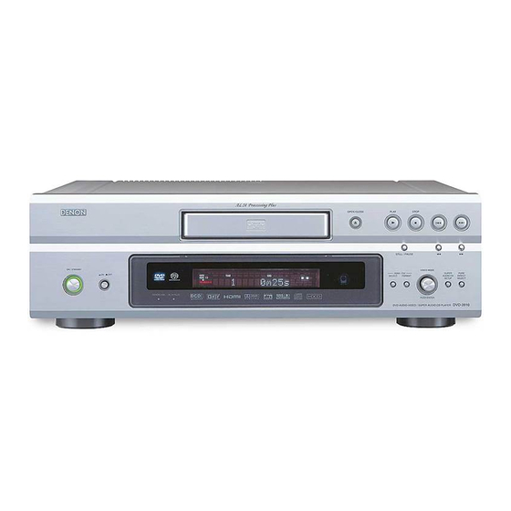
Denon DVD-3910 Service Manual
Dvd audio-video/ super audio cd player
Hide thumbs
Also See for DVD-3910:
- Operating instructions manual (158 pages) ,
- Specifications (2 pages) ,
- Specification (36 pages)
Table of Contents
Advertisement
QQ
3 7 63 1515 0
MODEL
DVD AUDIO-VIDEO / SUPER AUDIO CD PLAYER
TE
L 13942296513
For purposes of improvement, specifications and
design are subject to change without notice.
Please use this service manual with referring to the
operating instructions without fail.
Some illustrations using in this service manual are
slightly different from the actual set.
www
.
http://www.xiaoyu163.com
SERVICE MANUAL
DVD-3910
x
ao
u163
y
i
http://www.xiaoyu163.com
2 9
8
For U.S.A., Canada, Europe, Asia,
& Japan model
Q Q
3
6 7
1 3
1 5
co
Tokyo, Japan
.
9 4
2 8
0 5
8
2 9
9 4
2 8
m
X0200V.01 DE/CDM 0407
9 9
9 9
Advertisement
Table of Contents

Related Manuals for Denon DVD-3910


Summary of Contents for Denon DVD-3910
- Page 1 3 7 63 1515 0 For U.S.A., Canada, Europe, Asia, & Japan model SERVICE MANUAL DVD-3910 MODEL DVD AUDIO-VIDEO / SUPER AUDIO CD PLAYER L 13942296513 For purposes of improvement, specifications and design are subject to change without notice.
- Page 2 DVD-3910 3 7 63 1515 0 SAFETY PRECAUTIONS LEAKAGE CURRENT CHECK LASER RADIATION 500V L 13942296513 u163 http://www.xiaoyu163.com...
- Page 3 DVD-3910 WIRE ARRANGEMENT 3 7 63 1515 0 If wire bundles are untied or moved to perform adjustment or parts replacement etc.,be sure to rearrange them neatly as they were originally bundled or placed afterward. Otherwise, incorrect arrangement can be a cause of noise generation.
- Page 4 DVD-3910 DISASSEMBLY 3 7 63 1515 0 (Follow the procedure below in reverse order when reas- sembling.) (Disassembly and abandonment) (1)Disassembly of a set 1. 11. It decomposes according to a work procedure 1. 11. clause. (c, , ,...
- Page 5 DVD-3910 3 7 63 1515 0 1. Top cover (1)Remove 2 screws(s 1) on the rear side and 9 screws(s 2) on the top and the both sides. Remove 2-washer at the front center on the top. (2)Widen the Top cover a little laterally, then detach it m 1 Top cover with sliding.
- Page 6 DVD-3910 3 7 63 1515 0 3.DVD mechanism ass'y (1)Remove 4 screws(s 3) on the top side. (2)Disconect [CY251] [CY301] [CY171] [CX331] [CY101] from the MAIN P.W.B.(GU-3618). (3)Take the DVD mechanism ass'y(c 2) off. c 2 DVD mechanism ass'y 4.Power P.W.B.
- Page 7 DVD-3910 3 7 63 1515 0 5.Video P.W.B. ass'y and Scart P.W.B. ass'y Video P.W.B. ass'y 5-1. (1)Remove 6 screws(s 1) and 2(Japan :3) screws(s 5) and 2 Nuts(s 6) on the rear side and 2 screws (s 3) on the top side.
- Page 8 DVD-3910 3 7 63 1515 0 7.IEEE1394 sub ass'y (1)Remove 2 rear screws(s 1) and 1 top screw(s 3). (2)Disconnect [CY071] [CY173] [CY191]. (3)Remove 2 top screws(s 1) . (4)Take the IEEE1394 P.W.B. ass'y(c 9) off. BASS RUBBER(S) (only JAPAN) 3 Ieee1394 top Shield P.W.B.
- Page 9 DVD-3910 3 7 63 1515 0 9.Rear panel and Mecha base Rear panel 9-1. (1)Remove 5 rear screws(s 1) and and 2 top screws (s 1). (2)Take the Rear panel(m 5) off. 9-2.Mecha base (1)Remove 6 screws(s 1) on the top side.
- Page 10 DVD-3910 3 7 63 1515 0 11.Parts on Front panel sub ass'y(a.1) Display P.W.B. ass'y 11-1. (1)Remove 7 screws(s 7). (2)Disconnect [CX052] . (3)Detach D12mm knob ass'y(c 11). (4)Take the Display P.W.B. ass'y(c 12) off. 11-2.Power SW-1 P.W.B. ass'y (1)Remove 2 screws(s 7).
- Page 11 DVD-3910 3 7 6 3 1 5 1 5 0 op Measurement (Judging for Traverse Unit Replacement) As to deciding whether optical pickup is defect or not (for replacing traverse unit), follow the steps below. 1. Judging Step (1) Disc play abnormal Problems such as disc no read, unsteady playback, etc.
- Page 12 DVD-3910 3 7 6 3 1 5 1 5 0 DIAGNOSTICS OF OPTICAL PICKUP AND REPLACING TRAVERSE UNIT 1. Note for Handling the Laser Pick-up The protection for the damage of laser diode. If you want to change the optical device unit from any other units, you must keep the following.
- Page 13 DVD-3910 3 7 6 3 1 5 1 5 0 How to Replace Traverse Unit 1. Preparing for Replacement (1) Removing Clamp Base Damper Remove 4 pcs of 2.6mm machine screw (a), and detach the Clamp Base Damper upward.
- Page 14 DVD-3910 3 7 6 3 1 5 1 5 0 3. Installing Loader Plate Gear (1) Inserting Loader Set and push the Loader to the arrow direction until it Boss stops. When installing the Loader, move the Plate Gear...
- Page 15 DVD-3910 3 7 6 3 1 5 1 5 0 5. Assembly (2) (1) Attaching Tape to Clamp Base Damper Attach acetate cloth tape to 3 projections of the Clamp Base Damper backside. Acetate Cloth Tape Clamp Base Damper...
-
Page 16: Service Mode
DVD-3910 SERVICE MODE 3 7 63 1515 0 1. Aging Mode (1) preparation (a) Equipment used: Any one of DVD Karaoke Disc (contain- ing more than 10 titles). (b) Unit setting : No spec other than the following procedure (Aging mode). - Page 17 DVD-3910 -Com Firm Check Mode 3 7 63 1515 0 (1) Preparation (a) Equipment used: None (b) Unit setting: No spec other than the following procedure. (2) Procedure (a) Press the “POWER” button to turn on the power while pressing the “PLAY”...
- Page 18 DVD-3910 4. Setting up the test mode 3 7 63 1515 0 (1) Setting up Firmware Change needs. • In order to set up the test mode, you press STOP button and REV button simultaneously in the heat-run mode.Fun- damentaly, you can set up the test mode at the stop state after disc loading.
- Page 19 DVD-3910 (b) In the case of trace mode (error rate display) (refer to ta- 3 7 63 1515 0 ble 2 trace mode details) FL display (The display part of 13 digits) (YY: select mode [71--94] ,F: address and an error rate display F at the...
- Page 20 DVD-3910 (7) Test mode detailed table 3 7 63 1515 0 Table 1: servo adjustment value display mode details L 13942296513 u163 http://www.xiaoyu163.com...
- Page 21 DVD-3910 3 7 63 1515 0 L 13942296513 u163 http://www.xiaoyu163.com...
- Page 22 DVD-3910 Table 2: trace mode details 3 7 63 1515 0 L 13942296513 u163 http://www.xiaoyu163.com...
- Page 23 DVD-3910 Table 3: 3 7 63 1515 0 Table 4: L 13942296513 u163 http://www.xiaoyu163.com...
- Page 24 DVD-3910 3 7 6 3 1 5 1 5 0 TROUBLE SHOOTING 1. GU-3618 (MAIN UNIT) ,GU-3613-1 (SYSTEM UNIT) 1. GU-3618 (MAIN UNIT) ,GU-3613-1 (SYSTEM UNIT) 1.1. FL TUBE dosen't light 1.1. FL (1) Check the Set-up process of System -COM (IC202) µ-COM (IC202)
- Page 25 DVD-3910 3 7 6 3 1 5 1 5 0 (2) Check the Set-up process of B/E -COM (2) Check the Set-up process of B/E -COM Check Power Supply Voltages. GU-3618(MAIN UNIT) Check the output level. Check Soldering. GU-3618(MAIN UNIT) [IC108]:D1,D4 [IC202]:88pin.
- Page 26 R618 and R628 [IC507]:(DRVRST)51pin R618 and R628 "H"level O.K.? "H"level O.K.? O.K. O.K. 1.2. Image is not displayed.(Blue-back,DENON wallpaper) 1.2. DENON Check Digital output signal for Video.[1] 1 3 9 4 2 2 9 6 5 1 3 GU-3618(MAIN UNIT) Check Soldering.
- Page 27 DVD-3910 3 7 6 3 1 5 1 5 0 1.3. Does not Read Disc 1.3. [No Play],[00 00] displayed etc. [No Play],[00 00] (1) Disc does not Rotate. Check the Emission of Pick-up. (1) Check Soldering of P.U.
- Page 28 DVD-3910 3 7 6 3 1 5 1 5 0 (4) SACD check process (4) SACD Check Power Supply Voltages. Check Soldering. GU-3618(MAIN UNIT) [IC950] GU-3618(MAIN UNIT) [IC950] [IC401],[IC403],[IC405]: FB952,FB956 [IC401],[IC403],[IC405]: FB952,FB956 +5V_A2,+3.3V_D2,+2.5V_D2 O.K.? +5V_A2,+3.3V_D2,+2.5V_D2 O.K.? O.K. O.K. Check Clock waveform.
- Page 29 DVD-3910 3 7 6 3 1 5 1 5 0 1.4. No Sound,Noise generated 1.4. (1) CD,DVD-VIDEO/AUDIO (1) CD,DVD-VIDEO/AUDIO Check PCM Digital Audio Data(VSTEM data) Check Soldering. /VSTEM and VSTEM communication. [IC401]:75-98pin [IC401]:75-98pin GU-3618(MAIN UNIT) R401-R412,R494 GU-3618(MAIN UNIT) R401-R412,R494...
- Page 30 DVD-3910 3 7 6 3 1 5 1 5 0 (2) SACD : SOURCE DIRECT ON MODE (2) SACD : SOURCE DIRECT ON MODE Check SACD Digital Audio Data(VSTEM data) Check Soldering. SACD /VSTEM and VSTEM communication. [IC401]:35-37,44-48,54,63,67-69pin [IC401]:35-37,44-48,54,63,67-69pin...
- Page 31 DVD-3910 3 7 6 3 1 5 1 5 0 GU-3613-1 (SYSTEM UNIT)/GU-3614 (AUDIO UNIT) GU-3613-1 (SYSTEM UNIT)/GU-3614 (AUDIO UNIT) CD,DVD-VIDEO/AUDIO,(SACD-SOURCE DIRECT OFF) CD,DVD-VIDEO/AUDIO,(SACD-SOURCE DIRECT OFF) Check connection Mecha UNIT Check Soldering. FFC cable N.G. [CX301] N.G. [CX301] GU-3613-1(SYSTEM UNIT)
- Page 32 DVD-3910 3 7 6 3 1 5 1 5 0 SACD-SOURCE DIRECT ON SACD-SOURCE DIRECT ON Check connection Mecha UNIT Check Soldering. FFC cable N.G. [CX301] N.G. [CX301] GU-3613-1(SYSTEM UNIT) [CY302]:GU-3618 GU-3613-1(SYSTEM UNIT) [CY302]:GU-3618 [CX301]output signal FFC cable insert condition [CX301] O.K.
- Page 33 DVD-3910 3 7 6 3 1 5 1 5 0 3. GU-3613-2 (VIDEO UNIT) 3. GU-3613-2 (VIDEO UNIT) (1) Progressive output [Y,Pb,Pr] does not outputed. [Y,Pb,Pr] Check Power Supply Voltages. GU-3613-2(VIDEO UNIT) Check Soldering. GU-3613-2(VIDEO UNIT) +3.3V_D3, +5V_V1, +2.5V_V1, +1.8V_V1 [CY051],[IC715],[IC716] +3.3V_D3, +5V_V1, +2.5V_V1, +1.8V_V1...
- Page 34 DVD-3910 3 7 6 3 1 5 1 5 0 Check Video Buffer circuit. GU-3613-2(VIDEO UNIT) Check the soldering [TR701-TR703] GU-3613-2(VIDEO UNIT) [TR701-TR703] [TR701-TR703] and circumference soldering of [TR701-TR703]. [TR701-TR703] [VR702-VR704] [VR702-VR704] O.K. O.K. Check Video Driver circuit. GU-3613-2(VIDEO UNIT)
- Page 35 DVD-3910 ELECTRICAL ADJUSTMENT FOR VIDEO 3 7 63 1515 0 1. SETTING (1) Connect the monitor TV to the video output terminal. (2) Connect the oscilloscope to the Y-signal and C-signal of S-VIDEO output terminal and each terminate at 75 Ohms.
- Page 36 DVD-3910 2.3. Procedure 3 7 63 1515 0 (1) Adjust the signal of S-VIDEO out by the wave of oscillo- scope. (a) Target, Y-signal Point VR709 Adjustment Value 1000 20mV Waveform Y-signal of S-VIDEO out (b) Target, C-signal Point...
- Page 37 DVD-3910 (c) Target, P -signal 3 7 63 1515 0 Point VR704 Adjustment Value *525 10mV Waveform -signal * : 486 10mV for U.S.A. & Canada model L 13942296513 u163 http://www.xiaoyu163.com...
- Page 38 BLOCK DIAGRAM DVD-3910 3 7 6 3 1 5 1 5 0 1 3 9 4 2 2 9 6 5 1 3 w w w u 1 6 3 http://www.xiaoyu163.com...
- Page 39 DVD-3910 3 7 63 1515 0 SEMICONDUCTORS / Only major IC's are shown, general IC's etc. are omitted to list. Note: Abbreviation ahead of IC No. indicates the name of P.W.B., etc. MA: Main P.W.B. IE : IEEE1394 P.W.B.
- Page 40 DVD-3910 3 7 63 1515 0 Block Diagram 16/4M DRAM ECC Core Memory Data manager Slicer Demodulation Video MPEG I/F CD-DSP (DDCD) Data-PLL VSTEM Serial ASP Serial I/F VSTEM Serial I/F Command CD-ROM DSP CLK/Mode Header Dec. Spindle Audio I/F...
- Page 41 DVD-3910 3 7 63 1515 0 Terminal Name Classification Function 31 SYSCK Clock Clock Monitor output. 32 DV & GND Digital 1.8V Power. (Internal logic system power) 33 XI Clock Crystal oscillation input. 34 XO Clock Crystal oscillation output.
- Page 42 DVD-3910 3 7 63 1515 0 Terminal Name Classification Function 92 AD1 AD1 Input. 93 AD2 AD2 Input. 94 AV & GND Analog 3.3V Power. 95 AD3 AD3 Input. 96 AD4 AD4 Input. 97 AD5 AD5 Input. 98 AD6 AD6 Input.
- Page 43 DVD-3910 3 7 63 1515 0 Terminal Name Classification Function 150 RD14 DRAM I/F DRAM data input/output terminal 14. 151 RD13 DRAM I/F DRAM data input/output terminal 13. 152 RD12 DRAM I/F DRAM data input/output terminal 12. 153 RD11 DRAM I/F DRAM data input/output terminal 11.
- Page 44 DVD-3910 3 7 63 1515 0 ES6138F (MA: IC108) PINOUT DIAGRAM HA2/AUX4[4] DSCK I2CDATA/AUX[0] I2C_CLK/AUX[1] DCS0# AUX[2]/IOW# DCS1# AUX[3]/IOR# DB15 AUX[4] DB14 AUX[5] DB13 AUX[6] DB12 AUX[7] LOE# DB11 DB10 LCS0# LCS1# LCS2# LCS3# L 13942296513 ES6138F DMBS1 DMBS0...
- Page 45 DVD-3910 3 7 63 1515 0 ES6138F Pin Description Name Pin Numbers Definition 1,18, 27, 59, 68, 75, 92, 99, 104, 130, I/O power supply. 148, 157, 159, 164, 183, 193, 201 2:7, 10:16, 19:23, LA[21:0] RISC port address bus.
- Page 46 DVD-3910 3 7 63 1515 0 ES6138F Pin Description (Continued) Name Pin Numbers Definition TSD0 Audio transmit serial data port 0. SEL_PLL0 Refer to the description and matrix for SEL_PLL2 pin 32. TSD1 Audio transmit serial data port 1.
- Page 47 DVD-3910 3 7 63 1515 0 ES6138F Pin Description (Continued) Name Pin Numbers Definition DSCK Output clock to DRAM. DCLK Clock input to PLL. YUV0 YUV pixel 2 output data. CAMIN2 Camera YUV 2. UDAC Video DAC output. Value...
- Page 48 DVD-3910 3 7 63 1515 0 ES6138F Pin Description (Continued) Name Pin Numbers Definition ADVSS Analog ground for video DAC. YUV5 YUV pixel 5 output data. YDAC Video DAC output. Refer to description and matrix for UDAC pin 106.
- Page 49 DVD-3910 3 7 63 1515 0 ES6138F Pin Description (Continued) Name Pin Numbers Definition Host data bus line 9. AUX2[1] Aux2 data I/O. HD10 Host data bus line 10. AUX2[2] Aux2 data I/O. HD11 Host data bus line 11.
- Page 50 DVD-3910 3 7 63 1515 0 ES6138F Pin Description (Continued) Name Pin Numbers Definition HRD# Host read (active-low). DCI_ACK# DVD channel data valid (active-low). AUX4[6] Aux4 data I/O. HIOCS16# Device 16-bit data transfer (active-low). CAMCLK Camera port pixel clock input.
- Page 51 DVD-3910 3 7 63 1515 0 FLI2310 (SY: IC718) Block Diagrams Port 2 Noise Reducer, 8-bit Vertical and Output Input Processor Deinterlacer, Frame 656 Input Horizontal Processor with Auto Sync Rate Converter and Scalers and auto Adjust SDRAM interface...
- Page 52 DVD-3910 3 7 63 1515 0 Pin details Voltage Pull up/ No Pin Name I/O Type Tolerance Drive Pulldown Description Horizontal sync or reference -CTL1 of Port 1 HSYNC1_PORT1 Input Vertical sync or reference -CTL1 of Port 1 VSYNC1_PORT1...
- Page 53 DVD-3910 3 7 63 1515 0 Voltage Pull up/ No Pin Name I/O Type Tolerance Drive Pulldown Description 45 SCLK 8 mA 2-wire serial control bus clock 46 SDATA 8 mA 2-wire serial control bus data 47 RESET_N Reset...
- Page 54 DVD-3910 3 7 63 1515 0 Voltage Pull up/ No Pin Name I/O Type Tolerance Drive Pulldown Description 89 VSS Ground Ground 90 TEST IN Input Test input-Connect to ground 91 SDRAM ADDR(10) Tristate O/P 8 mA SDRAM address bus *...
- Page 55 DVD-3910 3 7 63 1515 0 Voltage Pull up/ No Pin Name I/O Type Tolerance Drive Pulldown Description 128 VDD7 Power 3.3 V – Power pin for IO 129 VSS Ground Ground 130 B/U/Pb_OUT_2 8 mA Digital video output – Blue/U/Pb Tristate O/P Digital video output –...
- Page 56 DVD-3910 3 7 63 1515 0 Voltage Pull up/ No Pin Name I/O Type Tolerance Drive Pulldown Description 172 DAC_AVSSB Ground Analog Ground for B channel 173 DAC_GOUT 34 mA Analog G/Y output Output 174 DAC_AVDDG Power 3.3 V – Analog power pin for G channel...
- Page 57 DVD-3910 3 7 63 1515 0 CXD2753R (MA: IC405) Pin Assignment L 13942296513 Block Diagram u163 http://www.xiaoyu163.com...
- Page 58 DVD-3910 3 7 63 1515 0 Pin Name Functions 1 VSC It fixed to ground.( for Core) Latch input for µCOM serial communication. 2 XMSLAT Shift clock input for µCOM serial communication. 3 MSCK Data input for µCOM serial communication.
- Page 59 DVD-3910 3 7 63 1515 0 Pin Name Functions 50 TESTO Output for TEST. (open) 51 TESTI Input for TEST. It fixed to “L” potential. 52 TESTI Input for TEST. It fixed to “L” potential. 53 TESTO Output for TEST. (open) 54 VDC +2.5V Power for CORE.
- Page 60 DVD-3910 3 7 63 1515 0 Pin Name Functions 96 TESTI TEST input terminal. It fixed to “L” potential. 97 TESTI TEST input terminal. It fixed to “H” potential. 98 TESTO TEST output terminal. (open) 99 VDC +2.5V Power for CORE.
- Page 61 DVD-3910 3 7 63 1515 0 Pin Name Functions 148 A11 Address output terminal for SDRAM. (MSB) 149 A10 Address output terminal for SDRAM. 150 VSC Ground for CORE. 151 A9 Address output terminal for SDRAM. 152 A8 Address output terminal for SDRAM.
- Page 62 DVD-3910 3 7 63 1515 0 ADSP-21266SKSTZ1B-DVD (SY: IC209) PIN 1 INDICATOR TOP VIEW Terminal Function LQFP LQFP LQFP LQFP Pin Name Pin # Pin Name Pin # Pin Name Pin # Pin Name Pin # DDINT DDINT DDEXT...
- Page 63 DVD-3910 3 7 63 1515 0 M30620FCPGP(3910) (SY: IC202) /CS0 /CS1 /CS2 /CS3 /WRL/WR /WRH/BHE /BCLK /HLDA /HOLD /ALE /RDY/CLK /CTS /RTS /CLK /RxD /CTS /RTS /CLKS /CLK /RxD AVcc /SDA/TA0 (Note) /RxD /SCL/TA0 /TB5 (Note) /ANEX1/S /ANEX0/CLK4 /CLK...
- Page 64 DVD-3910 3 7 63 1515 0 PIN Description FUNCTION PIN No DESCRIPTION PIN NAME SYMBOL TB4IN DSPSPICS DSP CONTROL SIGNAL V-CS VFD CONTROL SIGNAL(CS) / H=NEGATE , L=ASSERT SOUT3 V-DATA VFD CONTROL SIGNAL(DATA) SIN3 ROM CONT 1 NOT USED...
- Page 65 DVD-3910 3 7 63 1515 0 EXT_INT SPDIF OUTPUT CONTROL H=EXT IN, L=INT SW_HGAIN SUB WOOFER HGAIN BUSYEPROM DSP CONTROL (SPARE) NORMAL: "H" FLASH WRITING FOR DSP: "L" DSP_RST DSP RESET OUTPUT TERMINAL (RESET: "L") ROMRST MEMORY RESET FOR DSP (RESET: "L")
- Page 66 DVD-3910 3 7 63 1515 0 K4S643232E (SY: IC717) PIN CONFIGURATION BLOCK DIAGRAM DQ15 Data Input Register LDQM DQ14 DQ13 Bank Select DQ12 DQ11 512K x 32 DQ10 512K x 32 512K x 32 512K x 32 DQM0 DQM1 Column Decoder Latency &...
- Page 67 DVD-3910 3 7 63 1515 0 ADV7310 (SY: IC701,710) ADV7300 (MA: IC706) VDD_IO S_BLANK SET 1 VREF COMP1 DAC A DAC B DAC C TOP VIEW AGND DAC D DGND DAC E DAC F COMP2 SET 2 EXT_LF RESET ADV7310 Terminal Function Pin No.
- Page 68 DVD-3910 3 7 63 1515 0 SiI 170B (SY: IC721) Pin Diagram RESERVED SCLS SDAS ISEL/RST# MSEN SiI 170B HTPLG 64-Pin LQFP (Top View) CTL3 VSYNC HSYNC L 13942296513 VREF PGND2 Pin Diagram u163 http://www.xiaoyu163.com...
- Page 69 DVD-3910 3 7 63 1515 0 Pin Descriptions Input Pins Pin Name Pin # Type Description D23-D12 See Pin Upper 12 bits of 24-bit pixel bus. Mode controlled by configuration register bit: Diagram When BSEL = HIGH, this bus inputs the top half of the 24-bit pixel bus.
- Page 70 DVD-3910 3 7 63 1515 0 Differential Signal Data Pins Pin Name Pin # Type Description TX0+ Analog TMDS Low Voltage Differential Signal output data pairs. TX0- Analog These pins are tri-stated when PD# is asserted. TX1+ Analog TX1-...
- Page 71 DVD-3910 3 7 63 1515 0 TSB41AB2 (IE: IC111)) PAP PACKAGE (TOP VIEW) 47 46 45 44 43 40 39 38 37 36 35 34 33 AGND AGND AGND RESET FILTER0 TESTM FILTER1 PLLV TSB41AB2 PLLGND PLLGND C/LKON DGND...
- Page 72 DVD-3910 3 7 63 1515 0 CXD1881AR (MA: IC502) MEVO MLPF MIRR LDON CXD1881AR RFAC CDPD DVDPD COLD L 13942296513 DVDLD ATON ATOP RFSIN CD_E RFDC CD_F u163 http://www.xiaoyu163.com...
- Page 73 DVD-3910 3 7 63 1515 0 HOLDEN FCCR b7-0 AGC HOLD CDR b6 FBCR b6-0 RFCR b3 CGR b1 PROGRAMMABLE OUTPUT INHIBIT DVDRFP INPUT EQUALIZER FULL WAVE BIAS FILTER CHARGE DVDRFN RECTIFIER DIFFERENTIATOR PUMP RFSIN SIGR b7-4 RFCR b5-4...
- Page 74 DVD-3910 3 7 63 1515 0 Terminal Function Power Supply Pins Name Function Power for RF and serial port Power for servo GND for RF and serial port GND for servo Power for output buffer Reference Power for servo output...
- Page 75 DVD-3910 3 7 63 1515 0 Analog Pins Name Function RF AGC integration capacitor connecting terminal Differential phase tracking LPF terminal Differential phase tracking LPF terminal Lens shift offset cancel LPF terminal Lens shift offset cancel LPF terminal MIRR top hold terminal...
- Page 76 DVD-3910 3 7 63 1515 0 K4S641632 (MA: IC114) W986416DH (MA: IC103) DQ15 VssQ DQ14 DQ13 DQ12 DQ11 DQ10 LDQM UDQM A10/AP L 13942296513 Terminal Function Pin No. Pin Name Function Description 1, 14, 27 Power (+3.3V) Power for input buffers and logic circuit inside DRAM.
- Page 77 DVD-3910 3 7 63 1515 0 16M SDRAM (MA: IC402) 16M SDRAM (TSOP)-8 (DM: IC103, 104) K4S161622D-TC80 W981616AH-8 Terminal Function Pin No. Pin Name Symbol Function Power Supply/Ground Power and ground for the input buffer and the core logic...
- Page 78 DVD-3910 3 7 63 1515 0 FAN8042 (MA: IC503) Pin Assignments IN1+ DO1+ IN1- DO1- OUT1 DO2+ IN2+ DO2- IN2- DO3+ FAN8042 L 13942296513 OUT2 DO3- IN3+ DO4+ DO4- IN3- OUT3 DO5+ IN4+ DO5- u163 http://www.xiaoyu163.com...
- Page 79 DVD-3910 3 7 63 1515 0 Block Diagram OPOUT2 SVCC OPIN2+ OPIN1- OPIN1+ OPOUT1 VREF OPIN2- PVCC1 POWER SAVE IN1+ DO1+ 40 K DO1- IN1- 10 K DO2+ OUT1 10 K IN2+ DO2- 10 K IN2- DO3+ 10 K...
- Page 80 DVD-3910 3 7 63 1515 0 Pin Definitions Pin Number Pin Name Pin Function Descrition IN1+ CH1 op-amp input (+) IN1- CH1 op-amp input (-) OUT1 CH1 op-amp output IN2+ CH2 op-amp input (+) IN2- CH2 op-amp input (-)
- Page 81 DVD-3910 3 7 63 1515 0 M29W160EB70N6 (MA: IC104 IE: IC401) BYTE V SS DQ15A–1 A0-A19 Address Inputs DQ0-DQ7 Data Inputs/Outputs DQ14 DQ8-DQ14 Data Inputs/Outputs DQ13 DQ15A–1 Data Input/Output or Address Input DQ12 Chip Enable Output Enable V CC...
- Page 82 DVD-3910 3 7 63 1515 0 LC89057W (SY: IC213) EMPHA/UO AUDIO/VO XMODE RXOUT Microcontroller C bit, U bit 37 DO 36 RERR 24 SDIN 23 SLRCK Input Demodulation 22 SBCK Data Selector 21 RDATA & Selector 21 RDATA Lock Detect...
- Page 83 DVD-3910 3 7 63 1515 0 Pin Name Function XOUT X’tal osc. connecting output terminal X’tal osc. connection, external clock input terminal (24.576MHz or 12.288MHz) DVDD — Digital power DGND — Digital GND EMPHA/UO Emphasis information/U-data output/Chip address setting terminal...
- Page 84 DVD-3910 3 7 63 1515 0 SM5819A (MA: IC801) Pin Assignment VDDL DSBCK POFLR POCSW DSIFL POSLR DSIFR PLRCK DSICT PBCK DSISW DSISL VDDH MCKOUT DSISR DIRDSCK SYNC FMTPCM INIT DIRPCK VDDL BLOCK DIAGRAM DSIFL DSIFR DSICT DSISL MUTE...
- Page 85 DVD-3910 3 7 63 1515 0 PIN DESCRIPTION Input Name Property Description voltage − − VDDL 2.5V Core power supply PCM output rate select 1 SEL1FS 3.3V L: 2fs/4fs, H: fs PCM output rate select 2 SEL4FS 3.3V L: 2fs, H: 4fs...
- Page 86 DVD-3910 3 7 63 1515 0 Input Name Property Description voltage − DSIFL 3.3V DSD data input: front left-channel − DSIFR 3.3V DSD data input: front right-channel − DSICT 3.3V DSD data input: center channel − DSISW 3.3V DSD data input: subwoofer channel −...
- Page 87 DVD-3910 3 7 63 1515 0 IC61LV25616 (IE: IC402) Pin Description Symbol Pin Name A0~A17 Address Inputs I/O0-I/O15 Data Inputs/Outputs Chip Enable Input I/O0 I/O15 I/O1 Output Enable Input I/O14 I/O2 I/O13 Write Enable Input I/O3 I/O12 Lower-byte Control (I/O0-I/O7)
- Page 88 DVD-3910 3 7 63 1515 0 M11L16161SA (MA: IC505) PIN DESCRIPTIONS PIN NO. PIN NAME TYPE DESCRIPTION I/O0 I/O15 I/O1 I/O14 I/O2 I/O13 Address Input I/O3 I/O12 Row Address:A0~A9 A0~A9 Input 21,24 Column Address:A0~A9 I/O4 I/O11 I/O5 I/O10 Input...
- Page 89 DVD-3910 3 7 63 1515 0 BH7862F (SY: IC708) CTRAP COUT 75ohm TEST MUTE1 MUTE1 TEST 1.5-6M 75ohm MIXOUT MIXFB YTRAP CLAMP CLAMP PYIN 75ohm YOUT PYTRAP PYOUT 75ohm PbIN PYFB PrIN PbOUT 75ohm MUTE2 N.C. L 13942296513 MUTE2...
- Page 90 DVD-3910 3 7 63 1515 0 PCM1796 (SY: IC221,222 AP: IC311,312) (TOP VIEW) ZEROL ZEROR AGND3L MSEL L− LRCK DATA AGND2 DGND AGND1 R− AGND3R Terminal Functions TERMINAL DESCRIPTIONS DESCRIPTIONS NAME AGND1 − Analog ground (internal bias) AGND2 −...
- Page 91 DVD-3910 3 7 63 1515 0 I OUT L− LRCK Current V OUT L Segment DATA Audio I OUT L+ Data Input I/V and Filter V COM L Oversampling Advanced Digital Bias I REF Segment Filter V COM R...
- Page 92 DVD-3910 3 7 63 1515 0 CY2302 (IE: IC110,505 SY: IC205) Pin Configuration Block Diagram FBIN OUT2 External feedback connection to FBIN OUT1 OUT1 or OUT2, not both ÷Q Phase Charge Detector Pump Reference Input Loop Filter Output OUT1...
- Page 93 DVD-3910 3 7 63 1515 0 BR24L32F-W (MA: IC116) Block diagram 32kbit EEPROM array 8bit 12bit Address Slave word Data 12bits decoder address register register START STOP Control logic High voltage generator Vcc level detect Pin configuration BR24L32F-W L 13942296513...
- Page 94 DVD-3910 3 7 63 1515 0 TOP245Y (AP: IC901) Tab Internally Connected to SOURCE Pin DRAIN (D) CONTROL (C) INTERNAL SUPPLY SHUNT REGULATOR/ ERROR AMPLIFIER SOFT START 5.8 V 4.8 V 5.8 V INTERNAL UV I FB COMPARATOR V I (LIMIT)
- Page 95 DVD-3910 3 7 63 1515 0 TA76432FC (AP: IC902) LM1117MPX-1.8 (SY: IC101 IE: IC205) Block Diagram Connection Diagrams L 13942296513 u163 http://www.xiaoyu163.com...
- Page 96 DVD-3910 3 7 63 1515 0 L 13942296513 u163 http://www.xiaoyu163.com...
- Page 97 PRINTED WIRING BOADE DVD-3910 3 7 6 3 1 5 1 5 0 GU-3618 MAIN PWB UNIT 1 3 9 4 2 2 9 6 5 1 3 w w w u 1 6 3 COMPONENT SIDE http://www.xiaoyu163.com...
- Page 98 DVD-3910 3 7 6 3 1 5 1 5 0 1 3 9 4 2 2 9 6 5 1 3 w w w u 1 6 3 FOIL SIDE http://www.xiaoyu163.com...
- Page 99 DVD-3910 3 7 6 3 1 5 1 5 0 GU-3517A IEEE1394 UNIT A 1 3 9 4 2 2 9 6 5 1 3 w w w u 1 6 3 COMPONENT SIDE http://www.xiaoyu163.com...
- Page 100 DVD-3910 3 7 6 3 1 5 1 5 0 1 3 9 4 2 2 9 6 5 1 3 w w w u 1 6 3 FOIL SIDE http://www.xiaoyu163.com...
- Page 101 DVD-3910 3 7 6 3 1 5 1 5 0 SYSTEM UNIT 1 3 9 4 2 2 9 6 5 1 3 w w w u 1 6 3 COMPONENT SIDE http://www.xiaoyu163.com...
- Page 102 DVD-3910 3 7 6 3 1 5 1 5 0 1 3 9 4 2 2 9 6 5 1 3 w w w u 1 6 3 FOIL SIDE http://www.xiaoyu163.com...
- Page 103 DVD-3910 3 7 6 3 1 5 1 5 0 AUDIO/POWER UNIT 1 3 9 4 2 2 9 6 5 1 3 w w w u 1 6 3 COMPONENT SIDE http://www.xiaoyu163.com...
- Page 104 DVD-3910 3 7 6 3 1 5 1 5 0 1 3 9 4 2 2 9 6 5 1 3 w w w u 1 6 3 FOIL SIDE http://www.xiaoyu163.com...
- Page 105 DVD-3910 3 7 63 1515 0 NOTE FOR PARTS LIST Part indicated with the mark " " are not always in stock and possibly to take a long period of time for supplying, or in some case supplying of part may be refused.
- Page 106 DVD-3910 PARTS LIST OF P.W.B. UNIT ASS'Y (FOR U.S.A. & CANADA) 3 7 63 1515 0 GU-3618 MAIN UNIT ASS’Y Ref. No. Part No. Part Name Remarks SEMICONDUCTORS GROUP IC101 262 3046 902 TC7WH157FU IC104 262 3361 001 M29W160EB70N6...
- Page 107 DVD-3910 Ref. No. Part No. Part Name Remarks 3 7 63 1515 0 R125 247 2009 909 RM73B--472JT (1608) R126 247 2018 903 RM73B--0R0KT R127 247 2007 943 RM73B--102JT R128 247 2009 909 RM73B--472JT (1608) R129-135 247 2004 920...
- Page 108 DVD-3910 Ref. No. Part No. Part Name Remarks 3 7 63 1515 0 R439 247 2018 903 RM73B--0R0KT R440,441 247 2003 989 RM73B--330JT R442 247 2008 926 RM73B--222JT R443,444 247 2008 913 RM73B--202JT R445-449 247 2004 920 RM73B--470JT R450...
- Page 109 DVD-3910 Ref. No. Part No. Part Name Remarks 3 7 63 1515 0 R589 247 2010 969 RM73B--223JT R590 247 2008 900 RM73B--182JT R591 247 2011 997 RM73B--753JT R592 247 2012 925 RM73B--104JT R593 247 2011 942 RM73B--473JT R594...
- Page 110 DVD-3910 Ref. No. Part No. Part Name Remarks 3 7 63 1515 0 C110 257 0511 904 CK73F1H103ZT C111 257 0512 903 CK73F1E104ZT C112 257 0503 912 CC73CH1H9R0DT C115 257 4011 905 CE67C0J101MT (RV2) C116 257 0509 929 CK73B1H102KT...
- Page 111 DVD-3910 Ref. No. Part No. Part Name Remarks 3 7 63 1515 0 C218 257 0511 904 CK73F1H103ZT C401-407 257 0512 903 CK73F1E104ZT C409 257 0512 903 CK73F1E104ZT C410 257 4011 905 CE67C0J101MT (RV2) C411 257 0512 903 CK73F1E104ZT...
- Page 112 DVD-3910 Ref. No. Part No. Part Name Remarks 3 7 63 1515 0 C571 257 4012 917 CE67C1C220MT (RV2) C572 257 0511 904 CK73F1H103ZT C573,574 254 4655 906 CE67C0J220MT (RV2) C575 257 0511 904 CK73F1H103ZT C576 257 0509 929...
- Page 113 DVD-3910 Ref. No. Part No. Part Name Remarks 3 7 63 1515 0 C917 257 0512 903 CK73F1E104ZT C918 257 0511 904 CK73F1H103ZT C920,921 257 0512 903 CK73F1E104ZT C922 257 0511 904 CK73F1H103ZT C923 257 0512 903 CK73F1E104ZT C924...
- Page 114 DVD-3910 Ref. No. Part No. Part Name Remarks 3 7 63 1515 0 RA703,704 247 9007 920 MNR14=0R0JE0 X101 399 0619 906 X'TAL(27MHZ) 414 0963 003 EARTH PLATE GEN6609 FE/BE ROM SUB ASS'Y L 13942296513 u163 http://www.xiaoyu163.com...
- Page 115 DVD-3910 3 7 63 1515 0 GU-3517A IEEE1394 UNIT A ASS’Y Ref. No. Part No. Part Name Remarks SEMICONDUCTORS GROUP IC103 262 3268 900 SN74LVC00APW-EL2 IC104 262 3269 909 SN74LVC125APW-EL2 IC106 262 3260 908 FCX0-03(24.576M/30) IC108 262 3260 908 FCX0-03(24.576M/30)
- Page 116 DVD-3910 Ref. No. Part No. Part Name Remarks 3 7 63 1515 0 R159 247 2009 983 RM73B--103JT R160 247 2018 903 RM73B--0R0KT R161 247 2005 903 RM73B--101JT R174-188 247 2018 903 RM73B--0R0KT R189 247 2003 947 RM73B--220JT R190-192...
- Page 117 DVD-3910 Ref. No. Part No. Part Name Remarks 3 7 63 1515 0 R586 247 2006 902 RM73B--331JT (1608) R587,588 247 2018 903 RM73B--0R0KT R589,590 247 2012 925 RM73B--104JT R592 247 2018 903 RM73B--0R0KT R594 247 2018 903 RM73B--0R0KT...
- Page 118 DVD-3910 Ref. No. Part No. Part Name Remarks 3 7 63 1515 0 C217 257 4012 904 CE67C1C100MT (RV2B55 C218 257 0516 954 CK73B1E104KT C219,220 257 0509 929 CK73B1H102KT C221 257 0516 954 CK73B1E104KT C222 254 4655 906 CE67C0J220MT (RV2)
- Page 119 DVD-3910 Ref. No. Part No. Part Name Remarks 3 7 63 1515 0 C541,542 257 0509 929 CK73B1H102KT C543 257 0516 954 CK73B1E104KT C544,545 257 0509 929 CK73B1H102KT C546 257 0516 954 CK73B1E104KT C547 254 4660 946 CE67C1H010MT (RV2B55...
- Page 120 DVD-3910 3 7 63 1515 0 GU-3613 SYSTEM UNIT ASS’Y Ref. No. Part No. Part Name Remarks SEMICONDUCTORS GROUP IC101 262 3265 903 LM1117MPX-1.8 IC102 262 2977 933 BA50BC0FP-E2 IC104 262 3364 008 SII9030 IC201 262 3082 924 BD4730G-TR...
- Page 121 DVD-3910 Ref. No. Part No. Part Name Remarks 3 7 63 1515 0 TR225 273 0426 907 2SC2412KLNT146 TR226 273 0460 905 KTC2875B-RTK TR229,230 269 0082 902 DTC114EKT96 TR231 272 0161 900 2SB1412TL(PQR) TR701-703 271 0293 901 2SA1022-B TR713,714...
- Page 122 DVD-3910 Ref. No. Part No. Part Name Remarks 3 7 63 1515 0 R226-231 247 2004 920 RM73B--470JT R232,233 247 2018 903 RM73B--0R0KT R234 247 2003 947 RM73B--220JT R235,236 247 2004 920 RM73B--470JT R237 247 2005 903 RM73B--101JT R238-241...
- Page 123 DVD-3910 Ref. No. Part No. Part Name Remarks 3 7 63 1515 0 R381 247 2018 903 RM73B--0R0KT R382 247 2009 983 RM73B--103JT R383 247 2018 903 RM73B--0R0KT R384-386 247 2004 920 RM73B--470JT R387-394 247 2018 903 RM73B--0R0KT R396,397...
- Page 124 DVD-3910 Ref. No. Part No. Part Name Remarks 3 7 63 1515 0 R524-526 247 2007 985 RM73B--152JT R527 247 2008 913 RM73B--202JT R528-530 247 2007 985 RM73B--152JT R531 247 2008 913 RM73B--202JT R532-534 247 2007 985 RM73B--152JT R535...
- Page 125 DVD-3910 Ref. No. Part No. Part Name Remarks 3 7 63 1515 0 R728 247 2003 989 RM73B--330JT R729-732 247 2018 903 RM73B--0R0KT R737 247 2007 943 RM73B--102JT R738 247 2008 955 RM73B--302JT R743 247 2008 955 RM73B--302JT R746...
- Page 126 DVD-3910 Ref. No. Part No. Part Name Remarks 3 7 63 1515 0 R966,967 247 2009 983 RM73B--103JT R968 247 2018 903 RM73B--0R0KT R969,970 247 2011 942 RM73B--473JT R971,972 247 2018 903 RM73B--0R0KT R974,975 247 2009 983 RM73B--103JT R977...
- Page 127 DVD-3910 Ref. No. Part No. Part Name Remarks 3 7 63 1515 0 C226-229 257 0512 903 CK73F1E104ZT C230 257 0501 901 CK73B1H103KT (1608) C231 257 3006 924 CF73=1C103JT(ECHUB5) C232 257 0512 903 CK73F1E104ZT C233 257 4013 903 CE67C0J471MT (RV)
- Page 128 DVD-3910 Ref. No. Part No. Part Name Remarks 3 7 63 1515 0 C317 257 0512 903 CK73F1E104ZT C318 257 0509 929 CK73B1H102KT C319 257 0512 903 CK73F1E104ZT C320 257 0509 929 CK73B1H102KT C321 257 0512 903 CK73F1E104ZT C322...
- Page 129 DVD-3910 Ref. No. Part No. Part Name Remarks 3 7 63 1515 0 C409,410 257 4012 904 CE67C1C100MT (RV2B55 C411,412 257 0501 901 CK73B1H103KT (1608) C413-416 257 3006 911 CF73=1C104JT(ECHUB5) C417-420 257 4012 920 CE67C1C470MT (RV2) C421,422 257 0512 903...
- Page 130 DVD-3910 Ref. No. Part No. Part Name Remarks 3 7 63 1515 0 C706 257 0512 903 CK73F1E104ZT C707-710 247 2018 903 RM73B--0R0KT C716 257 0512 903 CK73F1E104ZT C717 257 4011 905 CE67C0J101MT (RV2) C718,719 257 0506 951 CC73CH1H101JT...
- Page 131 DVD-3910 Ref. No. Part No. Part Name Remarks 3 7 63 1515 0 C854 257 0512 903 CK73F1E104ZT C855 257 4011 905 CE67C0J101MT (RV2) C856 257 0501 901 CK73B1H103KT (1608) C858 257 4011 905 CE67C0J101MT (RV2) C859 257 0512 903...
- Page 132 DVD-3910 Ref. No. Part No. Part Name Remarks 3 7 63 1515 0 CX332 205 1170 945 33P FFC BASE(FMNBMTT CX401 205 1226 912 40P CONNECTOR(AXN3)S CY51 205 0343 058 5P CONN.BASE(KR-PH) CY131 205 1072 988 13P PH CON.BASE(TAPE...
- Page 133 DVD-3910 Ref. No. Part No. Part Name Remarks 3 7 63 1515 0 X731 399 0864 900 X'TAL(13.5MHZ) GEN6610 RADIATOR SUB ASS'Y GEN6633 ROM ASS'Y 21266-0 L 13942296513 u163 http://www.xiaoyu163.com...
- Page 134 DVD-3910 3 7 63 1515 0 GU-3614 AUDIO/POWER UNIT ASS’Y Ref. No. Part No. Part Name Remarks SEMICONDUCTORS GROUP IC101 262 3228 908 M66005AFP IC102 499 0306 001 GP1UE271XK IC301-310 263 0896 909 NJM2068MD-TE1 IC311,312 262 3362 903 PCM1796DBR...
- Page 135 DVD-3910 Ref. No. Part No. Part Name Remarks 3 7 63 1515 0 LD104,105 393 9576 903 SELU1E10CXM-002 TH901 279 0044 002 NTH11D8R0LA RESISTORS GROUP R101-103 247 2006 902 RM73B--331JT (1608) R104 247 2009 983 RM73B--103JT R106 247 2009 938...
- Page 136 DVD-3910 Ref. No. Part No. Part Name Remarks 3 7 63 1515 0 R397-404 247 2005 945 RM73B--151JT R405-407 247 2007 914 RM73B--751JT R408 247 2007 927 RM73B--821JT R409 247 2007 914 RM73B--751JT R410 247 2007 927 RM73B--821JT R411,412...
- Page 137 DVD-3910 Ref. No. Part No. Part Name Remarks 3 7 63 1515 0 C108 257 0501 901 CK73B1H103KT (1608) C109-111 257 0512 903 CK73F1E104ZT C115-118 257 0501 901 CK73B1H103KT (1608) C119 257 0511 904 CK73F1H103ZT C120 257 0509 929...
- Page 138 DVD-3910 Ref. No. Part No. Part Name Remarks 3 7 63 1515 0 C444 257 0516 954 CK73B1E104KT C445 255 4256 955 CQ93P2A103JT(NH2) C446 254 4313 950 CE04W1H101MT(ASF) C451 257 0501 901 CK73B1H103KT (1608) C453 257 0501 901 CK73B1H103KT (1608)
- Page 139 DVD-3910 Ref. No. Part No. Part Name Remarks 3 7 63 1515 0 CX24 205 0581 001 2P VH CONNECTOR BASE CX25 205 0581 056 2P VH CONNECTOR BASE CX31 205 0343 032 3P CONN.BASE(KR-PH) CX51 205 0343 058 5P CONN.BASE(KR-PH)
- Page 140 DVD-3910 PARTS LIST OF P.W.B. UNIT ASS'Y (FOR EUROPE) 3 7 63 1515 0 GU-3618 MAIN UNIT ASS’Y Refer to parts list for U.S.A. & CANADA. GU-3517A IEEE1394 UNIT A ASS’Y Refer to parts list for U.S.A. & CANADA.
- Page 141 DVD-3910 Ref. No. Part No. Part Name Remarks 3 7 63 1515 0 IC851 262 1793 901 TC4W53F IC852 263 1115 906 NJM2267M (TE2) IC853 262 0707 901 TC4053BF (TAPE) IC854 262 2534 907 BA7660FS-E2 TR101 269 0082 902...
- Page 142 DVD-3910 Ref. No. Part No. Part Name Remarks 3 7 63 1515 0 R135 247 2018 903 RM73B--0R0KT R140 247 2010 985 RM73B--273JT R141,142 247 2018 903 RM73B--0R0KT R199 247 2005 987 RM73B--221JT R200 247 2009 983 RM73B--103JT R201...
- Page 143 DVD-3910 Ref. No. Part No. Part Name Remarks 3 7 63 1515 0 R313-315 247 2003 989 RM73B--330JT R317-319 247 2008 955 RM73B--302JT R321 247 2009 983 RM73B--103JT R323-331 247 2005 903 RM73B--101JT R332 247 2007 943 RM73B--102JT R334...
- Page 144 DVD-3910 Ref. No. Part No. Part Name Remarks 3 7 63 1515 0 R469 247 2011 926 RM73B--393JT R470 247 2007 943 RM73B--102JT R471 247 2008 926 RM73B--222JT R472 247 2005 903 RM73B--101JT R473-477 247 2018 903 RM73B--0R0KT R478...
- Page 145 DVD-3910 Ref. No. Part No. Part Name Remarks 3 7 63 1515 0 R645 247 2009 983 RM73B--103JT R646,647 247 2012 925 RM73B--104JT R648,649 247 2018 903 RM73B--0R0KT R651 247 2012 925 RM73B--104JT R652 247 2005 903 RM73B--101JT R656,657...
- Page 146 DVD-3910 Ref. No. Part No. Part Name Remarks 3 7 63 1515 0 R869 247 2005 987 RM73B--221JT R871-876 247 2005 945 RM73B--151JT R877,878 247 2005 987 RM73B--221JT R879-881 247 2003 989 RM73B--330JT R882,883 247 2005 987 RM73B--221JT R884,885...
- Page 147 DVD-3910 Ref. No. Part No. Part Name Remarks 3 7 63 1515 0 C133 257 4012 904 CE67C1C100MT (RV2B55 C134 257 0512 903 CK73F1E104ZT C135 257 0509 929 CK73B1H102KT C136 257 4012 904 CE67C1C100MT (RV2B55 C137 257 0512 903...
- Page 148 DVD-3910 Ref. No. Part No. Part Name Remarks 3 7 63 1515 0 C275 257 4012 920 CE67C1C470MT (RV2) C276 257 0509 929 CK73B1H102KT C277 257 0512 903 CK73F1E104ZT C282 257 0512 903 CK73F1E104ZT C283 257 0509 929 CK73B1H102KT...
- Page 149 DVD-3910 Ref. No. Part No. Part Name Remarks 3 7 63 1515 0 C358 254 4660 946 CE67C1H010MT (RV2B55 C359-361 254 4660 904 CE67C1H0R1MT (RV2B55 C362 257 0516 909 CK73B1E223KT C363 257 4011 905 CE67C0J101MT (RV2) C364 257 0512 903...
- Page 150 DVD-3910 Ref. No. Part No. Part Name Remarks 3 7 63 1515 0 C528 257 0509 929 CK73B1H102KT C529 257 0511 904 CK73F1H103ZT C530 257 0509 929 CK73B1H102KT C531 257 0511 904 CK73F1H103ZT C532 257 0509 929 CK73B1H102KT C533...
- Page 151 DVD-3910 Ref. No. Part No. Part Name Remarks 3 7 63 1515 0 C762 257 4011 905 CE67C0J101MT (RV2) C765 257 4011 905 CE67C0J101MT (RV2) C766 257 0516 954 CK73B1E104KT C767 254 4660 946 CE67C1H010MT (RV2B55 C768,769 254 4655 922...
- Page 152 DVD-3910 Ref. No. Part No. Part Name Remarks 3 7 63 1515 0 C903 257 0512 903 CK73F1E104ZT C905 257 4012 920 CE67C1C470MT (RV2) C906 257 4012 904 CE67C1C100MT (RV2B55 C908 257 0512 903 CK73F1E104ZT C910 257 4012 917...
- Page 153 DVD-3910 Ref. No. Part No. Part Name Remarks 3 7 63 1515 0 CX251 205 1170 961 25P FFC BASE(FMNBMTT CX301 205 1170 974 30P FFC BASE(FMNBMTT CX332 205 1170 945 33P FFC BASE(FMNBMTT CX401 205 1226 912 40P CONNECTOR(AXN3)S...
- Page 154 DVD-3910 Ref. No. Part No. Part Name Remarks 3 7 63 1515 0 RR857,858 247 2004 975 RM73B--750JT RR859 247 2018 903 RM73B--0R0KT RR860 247 2005 945 RM73B--151JT RR861 247 2018 903 RM73B--0R0KT RR862 247 2005 945 RM73B--151JT RR863...
- Page 155 DVD-3910 3 7 63 1515 0 GU-3614A AUDIO/POWER UNIT A ASS’Y Ref. No. Part No. Part Name Remarks SEMICONDUCTORS GROUP IC101 262 3228 908 M66005AFP IC102 499 0306 001 GP1UE271XK IC301-310 263 0896 909 NJM2068MD-TE1 IC311,312 262 3362 903...
- Page 156 DVD-3910 Ref. No. Part No. Part Name Remarks 3 7 63 1515 0 LD104,105 393 9576 903 SELU1E10CXM-002 TH901 279 0044 002 NTH11D8R0LA RESISTORS GROUP R101-103 247 2006 902 RM73B--331JT (1608) R104 247 2009 983 RM73B--103JT R106 247 2009 938...
- Page 157 DVD-3910 Ref. No. Part No. Part Name Remarks 3 7 63 1515 0 R397-404 247 2005 945 RM73B--151JT R405-407 247 2007 914 RM73B--751JT R408 247 2007 927 RM73B--821JT R409 247 2007 914 RM73B--751JT R410 247 2007 927 RM73B--821JT R411,412...
- Page 158 DVD-3910 Ref. No. Part No. Part Name Remarks 3 7 63 1515 0 C105 257 0506 951 CC73CH1H101JT C106 254 4299 964 CE04W1C470MT(SRE) C108 257 0501 901 CK73B1H103KT (1608) C109-111 257 0512 903 CK73F1E104ZT C115-118 257 0501 901 CK73B1H103KT (1608)
- Page 159 DVD-3910 Ref. No. Part No. Part Name Remarks 3 7 63 1515 0 C442 257 0516 954 CK73B1E104KT C443 257 0501 901 CK73B1H103KT (1608) C444 257 0516 954 CK73B1E104KT C445 255 4256 955 CQ93P2A103JT(NH2) C446 254 4313 950 CE04W1H101MT(ASF)
- Page 160 DVD-3910 Ref. No. Part No. Part Name Remarks 3 7 63 1515 0 AS905 417 0476 023 RADIATOR AS905 GEN6612 RADIATOR SUB ASS'Y CX24 205 0581 001 2P VH CONNECTOR BASE CX25 205 0581 056 2P VH CONNECTOR BASE...
- Page 161 DVD-3910 PARTS LIST OF P.W.B. UNIT ASS'Y (FOR ASIA) 3 7 63 1515 0 GU-3618 MAIN UNIT ASS’Y Refer to parts list for U.S.A. & CANADA. GU-3517A IEEE1394 UNIT A ASS’Y Refer to parts list for U.S.A. & CANADA.
- Page 162 DVD-3910 Ref. No. Part No. Part Name Remarks 3 7 63 1515 0 TR101 269 0082 902 DTC114EKT96 TR102 273 0460 905 KTC2875B-RTK TR103,104 269 0082 902 DTC114EKT96 TR105,106 273 0460 905 KTC2875B-RTK TR107 275 0110 905 HN1K02FU-TE85L TR201...
- Page 163 DVD-3910 Ref. No. Part No. Part Name Remarks 3 7 63 1515 0 R206 247 2018 903 RM73B--0R0KT R208 247 2009 983 RM73B--103JT R209 247 2018 903 RM73B--0R0KT R210 247 2009 983 RM73B--103JT R212 247 2005 987 RM73B--221JT R213...
- Page 164 DVD-3910 Ref. No. Part No. Part Name Remarks 3 7 63 1515 0 R339 247 2006 915 RM73B--271JT R340,341 247 2005 903 RM73B--101JT R342 247 2018 903 RM73B--0R0KT R343 247 2005 903 RM73B--101JT R351 247 2005 903 RM73B--101JT R353...
- Page 165 DVD-3910 Ref. No. Part No. Part Name Remarks 3 7 63 1515 0 R479 247 2008 984 RM73B--392JT R480 247 2018 903 RM73B--0R0KT R485,486 247 2007 943 RM73B--102JT R487 247 2005 987 RM73B--221JT R489 247 2018 903 RM73B--0R0KT R490...
- Page 166 DVD-3910 Ref. No. Part No. Part Name Remarks 3 7 63 1515 0 R659,660 247 2009 983 RM73B--103JT R661 247 2008 968 RM73B--332JT R662-665 247 2018 903 RM73B--0R0KT R666 247 2004 920 RM73B--470JT R667-669 247 2018 903 RM73B--0R0KT R673-677...
- Page 167 DVD-3910 Ref. No. Part No. Part Name Remarks 3 7 63 1515 0 R915 247 2007 943 RM73B--102JT R916,917 247 2003 989 RM73B--330JT R919-924 247 2009 983 RM73B--103JT R925-929 247 2018 903 RM73B--0R0KT R930,931 247 2003 989 RM73B--330JT R933...
- Page 168 DVD-3910 Ref. No. Part No. Part Name Remarks 3 7 63 1515 0 C201 257 0509 929 CK73B1H102KT C202,203 257 0512 903 CK73F1E104ZT C204 257 4011 905 CE67C0J101MT (RV2) C205 257 4012 917 CE67C1C220MT (RV2) C206 257 0512 903...
- Page 169 DVD-3910 Ref. No. Part No. Part Name Remarks 3 7 63 1515 0 C292,293 257 0512 903 CK73F1E104ZT C294 257 0502 955 CC73CH1H3R0CT C295,296 257 0509 929 CK73B1H102KT C297 257 0512 903 CK73F1E104ZT C298 257 0502 955 CC73CH1H3R0CT C299...
- Page 170 DVD-3910 Ref. No. Part No. Part Name Remarks 3 7 63 1515 0 C381 254 4658 958 CE67C1E101MT (RV) C382 257 0501 901 CK73B1H103KT (1608) C383 257 4011 905 CE67C0J101MT (RV2) C384 257 0501 901 CK73B1H103KT (1608) C385 257 0512 903...
- Page 171 DVD-3910 Ref. No. Part No. Part Name Remarks 3 7 63 1515 0 C541 257 0509 929 CK73B1H102KT C542 257 0511 904 CK73F1H103ZT C543 257 0509 929 CK73B1H102KT C544 257 0511 904 CK73F1H103ZT C545 257 0509 929 CK73B1H102KT C546...
- Page 172 DVD-3910 Ref. No. Part No. Part Name Remarks 3 7 63 1515 0 C781 254 4655 977 CE67C0J102MT (RV) C782 257 4011 905 CE67C0J101MT (RV2) C795 257 4011 905 CE67C0J101MT (RV2) C796,797 257 0512 903 CK73F1E104ZT C798 257 4011 905...
- Page 173 DVD-3910 Ref. No. Part No. Part Name Remarks 3 7 63 1515 0 OTHER PARTS GROUP AS203 417 0476 052 RADIATOR AS204 471 3304 015 3X8 CBS-Z CC101 257 0512 903 CK73F1E104ZT CN802 205 0375 000 10P CON.BASE(KR-PH) CX61,62 205 1072 946 6P PH CON.BASE...
- Page 174 DVD-3910 Ref. No. Part No. Part Name Remarks 3 7 63 1515 0 RA723-731 247 9002 909 MNR14=330JE0AB RA751,752 247 9007 920 MNR14=0R0JE0 RR201-204 247 2018 903 RM73B--0R0KT RR251 247 2018 903 RM73B--0R0KT RR701,702 247 2018 903 RM73B--0R0KT S202...
- Page 175 DVD-3910 3 7 63 1515 0 GU-3614D AUDIO/POWER UNIT D ASS’Y Ref. No. Part No. Part Name Remarks SEMICONDUCTORS GROUP IC101 262 3228 908 M66005AFP IC102 499 0306 001 GP1UE271XK IC301-310 263 0896 909 NJM2068MD-TE1 IC311,312 262 3362 903...
- Page 176 DVD-3910 Ref. No. Part No. Part Name Remarks 3 7 63 1515 0 TH901 279 0044 002 NTH11D8R0LA RESISTORS GROUP R101-103 247 2006 902 RM73B--331JT (1608) R104 247 2009 983 RM73B--103JT R106 247 2009 938 RM73B--622JT R107 247 2010 985...
- Page 177 DVD-3910 Ref. No. Part No. Part Name Remarks 3 7 63 1515 0 R405-407 247 2007 914 RM73B--751JT R408 247 2007 927 RM73B--821JT R409 247 2007 914 RM73B--751JT R410 247 2007 927 RM73B--821JT R411,412 247 2018 903 RM73B--0R0KT R413,414...
- Page 178 DVD-3910 Ref. No. Part No. Part Name Remarks 3 7 63 1515 0 C109-111 257 0512 903 CK73F1E104ZT C115-118 257 0501 901 CK73B1H103KT (1608) C119 257 0511 904 CK73F1H103ZT C120 257 0509 929 CK73B1H102KT C130 254 4533 950 CE04W0J471MT SMG/RE3...
- Page 179 DVD-3910 Ref. No. Part No. Part Name Remarks 3 7 63 1515 0 C445 255 4256 955 CQ93P2A103JT(NH2) C446 254 4313 950 CE04W1H101MT(ASF) C451 257 0501 901 CK73B1H103KT (1608) C453 257 0501 901 CK73B1H103KT (1608) C454 257 0509 929...
- Page 180 DVD-3910 Ref. No. Part No. Part Name Remarks 3 7 63 1515 0 CX25 205 0581 056 2P VH CONNECTOR BASE CX31 205 0343 032 3P CONN.BASE(KR-PH) CX51 205 0343 058 5P CONN.BASE(KR-PH) CX52 205 0355 059 5P KR CON BASE(L)
- Page 181 DVD-3910 PARTS LIST OF P.W.B. UNIT ASS'Y (FOR JAPAN) 3 7 63 1515 0 GU-3618 MAIN UNIT ASS’Y Refer to parts list for U.S.A. & CANADA. GU-3517A IEEE1394 UNIT A ASS’Y Refer to parts list for U.S.A. & CANADA.
- Page 182 DVD-3910 Ref. No. Part No. Part Name Remarks 3 7 63 1515 0 TR101 269 0082 902 DTC114EKT96 TR102 273 0460 905 KTC2875B-RTK TR103,104 269 0082 902 DTC114EKT96 TR105,106 273 0460 905 KTC2875B-RTK TR107 275 0110 905 HN1K02FU-TE85L TR201...
- Page 183 DVD-3910 Ref. No. Part No. Part Name Remarks 3 7 63 1515 0 R200 247 2009 983 RM73B--103JT R201 247 2003 989 RM73B--330JT R202-204 247 2009 983 RM73B--103JT R205 247 2004 920 RM73B--470JT R206 247 2018 903 RM73B--0R0KT R208...
- Page 184 DVD-3910 Ref. No. Part No. Part Name Remarks 3 7 63 1515 0 R332 247 2007 943 RM73B--102JT R334 247 2005 945 RM73B--151JT R336 247 2005 961 RM73B--181JT R337 247 2005 903 RM73B--101JT R338 247 2018 903 RM73B--0R0KT R340,341...
- Page 185 DVD-3910 Ref. No. Part No. Part Name Remarks 3 7 63 1515 0 R472 247 2005 903 RM73B--101JT R473-477 247 2018 903 RM73B--0R0KT R478 247 2008 900 RM73B--182JT R479 247 2008 984 RM73B--392JT R480 247 2018 903 RM73B--0R0KT R485,486...
- Page 186 DVD-3910 Ref. No. Part No. Part Name Remarks 3 7 63 1515 0 R651 247 2012 925 RM73B--104JT R652 247 2005 903 RM73B--101JT R656,657 247 2018 903 RM73B--0R0KT R659,660 247 2009 983 RM73B--103JT R661 247 2008 968 RM73B--332JT R662-665...
- Page 187 DVD-3910 Ref. No. Part No. Part Name Remarks 3 7 63 1515 0 R860 247 2009 983 RM73B--103JT R864 247 2008 955 RM73B--302JT R867 247 2007 901 RM73B--681JT R869 247 2005 987 RM73B--221JT R877,878 247 2005 987 RM73B--221JT R882,883...
- Page 188 DVD-3910 Ref. No. Part No. Part Name Remarks 3 7 63 1515 0 C137 257 0512 903 CK73F1E104ZT C138-141 257 0509 929 CK73B1H102KT C142 257 4012 904 CE67C1C100MT (RV2B55 C143,144 257 0512 903 CK73F1E104ZT C145-147 257 0509 929 CK73B1H102KT...
- Page 189 DVD-3910 Ref. No. Part No. Part Name Remarks 3 7 63 1515 0 C283 257 0509 929 CK73B1H102KT C284 257 0512 903 CK73F1E104ZT C285 257 0509 929 CK73B1H102KT C286 257 4013 903 CE67C0J471MT (RV) C287 257 0509 929 CK73B1H102KT...
- Page 190 DVD-3910 Ref. No. Part No. Part Name Remarks 3 7 63 1515 0 C364 257 0512 903 CK73F1E104ZT C366 257 0516 909 CK73B1E223KT C368,369 254 4660 904 CE67C1H0R1MT (RV2B55 C372 257 0501 901 CK73B1H103KT (1608) C375 257 0506 951...
- Page 191 DVD-3910 Ref. No. Part No. Part Name Remarks 3 7 63 1515 0 C532 257 0509 929 CK73B1H102KT C533 257 0511 904 CK73F1H103ZT C534 257 0509 929 CK73B1H102KT C535 257 0512 903 CK73F1E104ZT C536 257 0511 904 CK73F1H103ZT C537...
- Page 192 DVD-3910 Ref. No. Part No. Part Name Remarks 3 7 63 1515 0 C768,769 254 4655 922 CE67C0J470MT (RV2) C771 257 0512 903 CK73F1E104ZT C772 254 4660 946 CE67C1H010MT (RV2B55 C774 257 0516 954 CK73B1E104KT C775,776 254 4655 951...
- Page 193 DVD-3910 Ref. No. Part No. Part Name Remarks 3 7 63 1515 0 C923 257 0509 929 CK73B1H102KT C925,926 257 0512 903 CK73F1E104ZT C927 257 0509 929 CK73B1H102KT C928 257 4012 904 CE67C1C100MT (RV2B55 C929,930 257 0512 903 CK73F1E104ZT...
- Page 194 DVD-3910 Ref. No. Part No. Part Name Remarks 3 7 63 1515 0 L101-103 235 0125 905 INDUCTOR(FLC32C220K) L702-706 235 0125 905 INDUCTOR(FLC32C220K) L711-714 235 0125 905 INDUCTOR(FLC32C220K) L716,717 235 0125 905 INDUCTOR(FLC32C220K) L719-722 235 0125 905 INDUCTOR(FLC32C220K) RA101-106...
- Page 195 DVD-3910 3 7 63 1515 0 GU-3614B AUDIO/POWER UNIT B ASS’Y Ref. No. Part No. Part Name Remarks SEMICONDUCTORS GROUP IC101 262 3228 908 M66005AFP IC102 499 0306 001 GP1UE271XK IC301-310 263 0896 909 NJM2068MD-TE1 IC311,312 262 3362 903...
- Page 196 DVD-3910 Ref. No. Part No. Part Name Remarks 3 7 63 1515 0 LD104,105 393 9576 903 SELU1E10CXM-002 TH901 279 0044 002 NTH11D8R0LA RESISTORS GROUP R101-103 247 2006 902 RM73B--331JT (1608) R104 247 2009 983 RM73B--103JT R106 247 2009 938...
- Page 197 DVD-3910 Ref. No. Part No. Part Name Remarks 3 7 63 1515 0 R397-404 247 2005 945 RM73B--151JT R405-407 247 2007 914 RM73B--751JT R408 247 2007 927 RM73B--821JT R409 247 2007 914 RM73B--751JT R410 247 2007 927 RM73B--821JT R411,412...
- Page 198 DVD-3910 Ref. No. Part No. Part Name Remarks 3 7 63 1515 0 C108 257 0501 901 CK73B1H103KT (1608) C109-111 257 0512 903 CK73F1E104ZT C115-118 257 0501 901 CK73B1H103KT (1608) C119 257 0511 904 CK73F1H103ZT C120 257 0509 929...
- Page 199 DVD-3910 Ref. No. Part No. Part Name Remarks 3 7 63 1515 0 C444 257 0516 954 CK73B1E104KT C445 255 4256 955 CQ93P2A103JT(NH2) C446 254 4313 950 CE04W1H101MT(ASF) C451 257 0501 901 CK73B1H103KT (1608) C453 257 0501 901 CK73B1H103KT (1608)
- Page 200 DVD-3910 Ref. No. Part No. Part Name Remarks 3 7 63 1515 0 CX24 205 0581 001 2P VH CONNECTOR BASE CX25 205 0581 056 2P VH CONNECTOR BASE CX31 205 0343 032 3P CONN.BASE(KR-PH) CX51 205 0343 058 5P CONN.BASE(KR-PH)
- Page 201 EXPLODED VIEW DVD-3910 3 7 6 3 1 5 1 5 0 Parts List European model only Japan model only Adhesive : DIABOND DB-1616 Adhesive : DIABOND DB-1616 AV-1 5.1ch AUDIO OUT 2ch AUDIO OUT VIDEO OUT (AUDIO) E1 & E2...
- Page 202 23 00D4124944006 FRONT ANGLE 23 00D4124944006 FRONT ANGLE JP Model 24 00D1442891504 FRONT PANEL(BK) Black Model u163 24 00D1442891517 FRONT PANEL(GO) Gold Model 24 00D1442891520 FRONT PANEL(SR) Silver Model 25 00D1310158007 DENON BADGE Black Model 25 00D1310158010 DENON BADGE Gold Model http://www.xiaoyu163.com...
- Page 203 43 00D1462367005 LOADER PANEL(BK) Black Model 43 00D1462367018 LOADER PANEL(GO) Gold Model 43 00D1462367021 LOADER PANEL(SR) Silver Model 44 00D1350071005 DENON LINK BADGE Black Model 44 00D1350071018 DENON LINK BADGE Silver Model 44 00D1350071021 DENON LINK BADGE Gold Model 45 00D4770231024 4W(S) 10.0/4.2mm, t0.3 MECHA FOOT...
- Page 204 DVD-3910 Ref. No. Part No. Part Name Remarks Q'ty New 3 7 63 1515 0 WIRES 100 00D0090186015 24P FFC(0.5) PU CX241 101 00D0090251005 17P FFC(1.0) BDX10 IEEE1394 CW173 L=100 102 00D0090251018 17P FFC(1.0) BDX15 HDMI CW174 L=100 103 00D0090251021 17P FFC(1.0) BDX10 MAIN CW171 L=120 104 00D0090251034 19P FFC(1.0) BDX10...
- Page 205 DVD-3910 Ref. No. Part No. Part Name Remarks Q'ty New 3 7 63 1515 0 204 00D4737015005 3X6 CBTS(S)-B 205 00D4737500044 3X8 CBTS (P)-B 206 00D4737508017 3X10 CBTS (P)-B 207 00D4738044004 SPECIAL SCREW 208 00D4753002005 4TWA 209 00D4770064123 FIXING SCREW...
- Page 206 EXPLODED VIEW OF DVD MECHANISM DVD-3910 3 7 6 3 1 5 1 5 0 1 3 9 4 2 2 9 6 5 1 3 w w w u 1 6 3 http://www.xiaoyu163.com...
- Page 207 DVD-3910 PARTS LIST OF DVD MECHANISM(FG180-1) 3 7 63 1515 0 Ref. No. Part No. Part Name Remarks Q'ty 411 1988 101 Mecha chassis 431 0426 503 Plate gear 9KA 2A40 3D Gear base sub Ass'y 441 1952 109...
- Page 208 POINTS OF GREASING (1/2) DVD-3910 3 7 6 3 1 5 1 5 0 MOLYKOTE EM-30L 0.1mg x 2 points MOLYKOTE EM-30L 0.1mg MOLYKOTE EM-30L 1 3 9 4 2 2 9 6 5 1 3 0.1mg x 3 points MOLYKOTE EM-30L 0.1mg x 4 points...
- Page 209 POINTS OF GREASING (2/2) DVD-3910 3 7 6 3 1 5 1 5 0 MOLYKOTE EM-30L 0.1mg x 4 points HANARL FL777 0.1mg MOLYKOTE EM-30L MOLYKOTE EM-30L 0.1mg 0.1mg x 5 points MOLYKOTE EM-30L 1 3 9 4 2 2 9 6 5 1 3 0.3mg...
- Page 210 DVD-3910 PACKING VIEW 3 7 63 1515 0 L 13942296513 u163 http://www.xiaoyu163.com...
- Page 211 DVD-3910 PARTS LIST OF PACKING & ACCESSORIES Note: The symbols in the column ”Remarks” indicate 3 7 63 1515 0 the following destinations. E3 : U.S.A. & Canada model E2 : Europe model E1 : Asia model JP : Japan model Ref.No.
- Page 212 WIRING DIAGRAM DVD-3910 3 7 6 3 1 5 1 5 0 1 3 9 4 2 2 9 6 5 1 3 w w w u 1 6 3 http://www.xiaoyu163.com...
- Page 213 DVD-3910 MEASURING METHOD AND WAVEFORMS 3 7 63 1515 0 To check the waveforms on the Main P.W.B., the GND (-) probe of the oscilloscope to “Vref” point. (Except for lnner SW, TRVSW) NOTES Measuring Disc: DVD/DVDT-S01 or TDV-520A...
- Page 214 DVD-3910 WAVEFORMS 3 7 63 1515 0 DVD PLAY Disc: TDV-520A CD PLAY DISC DETECT (CD) FSCON TSCON RFAC VC16 MIRR DVD PLAY (INNER) CD PLAY Disc: TCD-784 RFAC VC16 CD PLAY (INNER) DVD LOADING PLAY L 13942296513 FSCON...
- Page 215 DVD-3910 3 7 63 1515 0 L 13942296513 u163 http://www.xiaoyu163.com...
- Page 216 DVD-3910 NOTE FOR SCHEMATIC DIAGRAM 3 7 63 1515 0 1. WARNING: Parts marked with this symbol have critical character- istics. Use ONLY replacement parts recommended by the manu- facturer. 2. CAUTION: Before returning the unit to the customer, make sure you make either (1) a leakage current check or (2) a line to µ...
- Page 217 DVD-3910 3 7 6 3 1 5 1 5 0 SCHEMATIC DIAGRAMS (1/22) 1 3 9 4 2 2 9 6 5 1 3 w w w u 1 6 3 SCHEMATIC DIAGRAMS (1/22) 00DGU-3618 MAIN PWB UNIT (1/4) SIGNAL LINE http://www.xiaoyu163.com...
- Page 218 DVD-3910 3 7 6 3 1 5 1 5 0 SCHEMATIC DIAGRAMS (2/22) 1 3 9 4 2 2 9 6 5 1 3 w w w u 1 6 3 SCHEMATIC DIAGRAMS (2/22) 00DGU-3618 MAIN PWB UNIT (2/4) SIGNAL LINE http://www.xiaoyu163.com...
- Page 219 DVD-3910 3 7 6 3 1 5 1 5 0 SCHEMATIC DIAGRAMS (3/22) 1 3 9 4 2 2 9 6 5 1 3 w w w u 1 6 3 SCHEMATIC DIAGRAMS (3/22) 00DGU-3618 MAIN PWB UNIT (3/4) SIGNAL LINE http://www.xiaoyu163.com...
- Page 220 DVD-3910 3 7 6 3 1 5 1 5 0 SCHEMATIC DIAGRAMS (4/22) 1 3 9 4 2 2 9 6 5 1 3 w w w u 1 6 3 SCHEMATIC DIAGRAMS (4/22) 00DGU-3618 MAIN PWB UNIT (4/4)
- Page 221 DVD-3910 3 7 6 3 1 5 1 5 0 SCHEMATIC DIAGRAMS (5/22) 1 3 9 4 2 2 9 6 5 1 3 w w w u 1 6 3 SCHEMATIC DIAGRAMS (5/22) SYSTEM UNIT (1/3) SIGNAL LINE...
- Page 222 DVD-3910 3 7 6 3 1 5 1 5 0 SCHEMATIC DIAGRAMS (6/22) 1 3 9 4 2 2 9 6 5 1 3 w w w u 1 6 3 SCHEMATIC DIAGRAMS (6/22) SYSTEM UNIT (2/3) SIGNAL LINE...
- Page 223 DVD-3910 3 7 6 3 1 5 1 5 0 SCHEMATIC DIAGRAMS (7/22) 1 3 9 4 2 2 9 6 5 1 3 w w w u 1 6 3 SCHEMATIC DIAGRAMS (7/22) SYSTEM UNIT (3/3) SIGNAL LINE...
- Page 224 DVD-3910 3 7 6 3 1 5 1 5 0 SCHEMATIC DIAGRAMS (8/22) 1 3 9 4 2 2 9 6 5 1 3 w w w u 1 6 3 SCHEMATIC DIAGRAMS (8/22) VIDEO UNIT (1/4) http://www.xiaoyu163.com...
- Page 225 DVD-3910 3 7 6 3 1 5 1 5 0 SCHEMATIC DIAGRAMS (9/22) 1 3 9 4 2 2 9 6 5 1 3 w w w u 1 6 3 SCHEMATIC DIAGRAMS (9/22) VIDEO UNIT (2/4) http://www.xiaoyu163.com...
- Page 226 DVD-3910 3 7 6 3 1 5 1 5 0 SCHEMATIC DIAGRAMS (10/22) 1 3 9 4 2 2 9 6 5 1 3 w w w u 1 6 3 SCHEMATIC DIAGRAMS (10/22) VIDEO UNIT (3/4) http://www.xiaoyu163.com...
- Page 227 DVD-3910 3 7 6 3 1 5 1 5 0 SCHEMATIC DIAGRAMS (11/22) 1 3 9 4 2 2 9 6 5 1 3 w w w u 1 6 3 SCHEMATIC DIAGRAMS (11/22) VIDEO UNIT (4/4) http://www.xiaoyu163.com...
- Page 228 DVD-3910 3 7 6 3 1 5 1 5 0 SCHEMATIC DIAGRAMS (12/22) 1 3 9 4 2 2 9 6 5 1 3 w w w u 1 6 3 SCHEMATIC DIAGRAMS (12/22) HDMI TX UNIT http://www.xiaoyu163.com...
- Page 229 DVD-3910 3 7 6 3 1 5 1 5 0 SCHEMATIC DIAGRAMS (13/22) 1 3 9 4 2 2 9 6 5 1 3 w w w u 1 6 3 SCHEMATIC DIAGRAMS (13/22) SCART UNIT http://www.xiaoyu163.com...
- Page 230 DVD-3910 3 7 6 3 1 5 1 5 0 SCHEMATIC DIAGRAMS (14/22) 1 3 9 4 2 2 9 6 5 1 3 w w w u 1 6 3 SCHEMATIC DIAGRAMS (14/22) AUDIO UNIT SIGNAL LINE http://www.xiaoyu163.com...
- Page 231 DVD-3910 3 7 6 3 1 5 1 5 0 SCHEMATIC DIAGRAMS (15/22) 1 3 9 4 2 2 9 6 5 1 3 w w w u 1 6 3 SCHEMATIC DIAGRAMS (15/22) D.POWER UNIT / P.SW-1 UNIT...
- Page 232 DVD-3910 3 7 6 3 1 5 1 5 0 SCHEMATIC DIAGRAMS (16/22) 1 3 9 4 2 2 9 6 5 1 3 w w w u 1 6 3 SCHEMATIC DIAGRAMS (16/22) DISPLAY UNIT / P.SW-2 UNIT...
- Page 233 DVD-3910 3 7 6 3 1 5 1 5 0 SCHEMATIC DIAGRAMS (17/22) 1 3 9 4 2 2 9 6 5 1 3 w w w u 1 6 3 SCHEMATIC DIAGRAMS (17/22) 00DGU-3517A IEEE1394 UNIT A (1/6)
- Page 234 DVD-3910 3 7 6 3 1 5 1 5 0 SCHEMATIC DIAGRAMS (18/22) 1 3 9 4 2 2 9 6 5 1 3 w w w u 1 6 3 SCHEMATIC DIAGRAMS (18/22) 00DGU-3517A IEEE1394 UNIT A (2/6)
- Page 235 DVD-3910 3 7 6 3 1 5 1 5 0 SCHEMATIC DIAGRAMS (19/22) 1 3 9 4 2 2 9 6 5 1 3 w w w u 1 6 3 SCHEMATIC DIAGRAMS (19/22) 00DGU-3517A IEEE1394 UNIT A (3/6)
- Page 236 DVD-3910 3 7 6 3 1 5 1 5 0 SCHEMATIC DIAGRAMS (20/22) 1 3 9 4 2 2 9 6 5 1 3 w w w u 1 6 3 SCHEMATIC DIAGRAMS (20/22) 00DGU-3517A IEEE1394 UNIT A (4/6)
- Page 237 DVD-3910 3 7 6 3 1 5 1 5 0 SCHEMATIC DIAGRAMS (21/22) 1 3 9 4 2 2 9 6 5 1 3 w w w u 1 6 3 SCHEMATIC DIAGRAMS (21/22) 00DGU-3517A IEEE1394 UNIT A (5/6)
- Page 238 DVD-3910 3 7 6 3 1 5 1 5 0 SCHEMATIC DIAGRAMS (22/22) 1 3 9 4 2 2 9 6 5 1 3 w w w u 1 6 3 SCHEMATIC DIAGRAMS (22/22) 00DGU-3517A IEEE1394 UNIT A (6/6)
Need help?
Do you have a question about the DVD-3910 and is the answer not in the manual?
Questions and answers